More Related Content
Similar to Transistor Models: Emitter Follower, Common Base & Hybrid Equivalent
Similar to Transistor Models: Emitter Follower, Common Base & Hybrid Equivalent (20)
More from Ismael Cayo Apaza
More from Ismael Cayo Apaza (20)
Transistor Models: Emitter Follower, Common Base & Hybrid Equivalent
- 1. © Copy Right: Rai University
4A.273 23
ELECTRONICDESIGNTECHNOLOGY
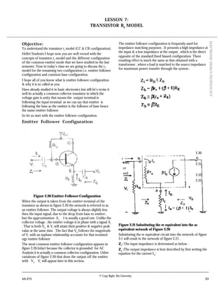
The emitter follower configuration is frequently used for
impedance matching purposes . It presents a high impedance at
the input & a low impedance at the output , which is the direct
opposite of the standard fixed biased configuration. There
resulting effect is much the same as that obtained with a
transformer , where a load is matched to the source impedance
for maximum power transfer through the system .
Figure 2.21 Substituting the re equivalent into the ac
equivalent network of Figure 2.20
Substituting the re equivalent circuit into the network of figure
3.1 will result in the network of figure 2.21 .
Zi
: The input impedance is determined as below :
Zo
:The output impedance is best described by first writing the
equation for the current Ib
:
Objective:
To understand the transistor re
model (CC & CB configuration).
Hello! Students I hope now you are well versed with the
concepts of transistor re
-model and the different configuration
of the common emitter mode that we have studied in the last
semester. Now in today’s class we are going to discuss the re
-
model for the remaining two configuration i.e. emitter follower
configuration and common base configuration.
I hope all of you know what is emitter follower configuration
& why it is so called as you.
Have already studied it in basic electronics but still let’s revise it
well its actually a common collector transistor in which the
voltage gain is unity that means the output terminal is
following the input terminal as we can say that emitter is
following the base as the emitter is the follower of base hence
the name emitter follower
So let us start with the emitter follower configuration.
Emitter Follower Configuration
Figure 2.20 Emitter-Follower Configuration
When the output is taken from the emitter terminal of the
transistor as shown in figure 2.20 the network is referred to as
an emitter follower. The output voltage is always slightly less
then the input signal, due to the drop from base to emitter ,
but the approximation Av
≅ 1 is usually a good one .Unlike the
collector voltage , the emitter voltage is in phase with a signal Ai
. That is both V0
& Vi
will attain their positive & negative peak
value at the same time . The fact that V0
follows the magnitude
of Vi
with an inphase relationship accounts for that terminol-
ogy emitter follower
The most common emitter follower configuration appears in
figure 2.20.Infact because the collector is grounded for AC
Analysis it is actually a common collector configuration. Other
variations of figure 2.20 that draw the output off the emitter
with V0
≅ Vi
will appear later in this section.
LESSON 7:
TRANSISTOR RE
MODEL
with
or
and
2.30
2.31
2.32
2.33
- 3. © Copy Right: Rai University
4A.273 25
ELECTRONICDESIGNTECHNOLOGY
Phase relationship :
As revealed by equation (2.37) and earlier discussion of this
section, Vo
and Vi
are in phase for the emitter follower configu-
ration.
Common Base Configuration
Common base configuration is characterized as having a
relatively low input and high output impedance and the current
gain less than 1. The voltage gain, however, can be quite large.
The standard configuration appears in Fig. 2.23 with the
common base re
equivalent model substituted in figure 2.24.
The transistor output impedance ro
is not included for the
common base configuration because it is typically in mega-
ohms range and can be ignored in parallel with resistance RC
.
The Hybrib Equivalent Model
The manufacturers specified the characteristics of a transistor in
terms of its h-paramrters. The word hybrid is used with these
parameters because they are a mixture of constants in different
units.
Transistor is a three terminal device. For each pair of terminals,
there are two variables (current & voltage). There are a number
of ways in which these variables can be related.
with 4.21
1
1 −≅−== α
I
v
A
- 4. 26 4A.273
© Copy Right: Rai University
ELECTRONICDESIGNTECHNOLOGY
V1
= h11
I1
+ h12
V2
I2
= h21
I1
+ h22
V2
Parameters h11
, h12
, h21
& h22
which relates the four variables of
the two port system are called hybrid parameters.These
parameters can be defined from the above equations by first
putting V2
= 0 (S.C. the output terminal) and then putting I1
=
0 (Opening the input terminal)
The suffix e is added to the symbols of h-parameters to
indicate that a transistor is used in CE-mode. In this mode
terminal 1 is the base terminal and 2 is the collector.
V1
and I1
becomes Ve
and Ie
and at the output port V2
and I2
becomes Vc
and Ic
Vb
= hie
Ib
+ hre
Vc
……………………………..(2.45)
Ic
= hfe
Ib
+ hoe
Vc
…………………………….(2.46)
Each term in equation 2.45 has units of volts therefore we can
use K.V.L. to find the circuit that fits in the equation (Fig. 2.26).
Each term in equation 2.46 has units of current.
Therefore, the complete AC equivalent of transistor using h-
parameters can be drawn as shown in Fig. 2.28.
Comparing the hybrid equivalent circuit with the transistor re
model we find, The only difference is the presence of a voltage
source hre
Vc
in the input of the hybrid model. The magnitude
of this voltage source depends on the output voltage Vc
.The
parameter hre
therefore represents a feedback of the output
voltage to the input circuit. In the normal operation of the
transistor this effect is very small, it will make practically no
difference if the term hre
Vc
is neglected from the hybrid
equivalent circuit.
Figure 2.26 Hybrid input
equivalent circuit.
Figure 2.27 Hybrid output
equivalent circuit.
hie
= 1K , hre
= 305 x 10-4
hfe
= 50 , hoe
= 25ms.
- 5. © Copy Right: Rai University
4A.273 27
ELECTRONICDESIGNTECHNOLOGY
- 6. 28 4A.273
© Copy Right: Rai University
ELECTRONICDESIGNTECHNOLOGY
Figure 2.28 Complete hybrid equivalent circuit of a
transistor
- 7. © Copy Right: Rai University
4A.273 29
ELECTRONICDESIGNTECHNOLOGY
The typical values of the hybrid parameters are
The topics covered during this lecture :
1. Emitter follower configuration
2. Common base configuration
3. Hybrid equivalent model
Now Answer these Questions:
1. Why is CC configuration is used in Impedance matching
purpose?
2. Give the basic characteristics of CB configuration.
3. What are hybrid parameters?
4. Whatishre
and how does it effect transistor operation?
Notes