SlideShare a Scribd company logo
1 of 15
Download to read offline
Electronic Circuits I Laboratory


2 DIODE CLIPPING and CLAMPING CIRCUITS

2.1 Objectives

   •    Understanding the operating principle of diode clipping circuit
   •    Understanding the operating principle of clamping circuit
   •    Understanding the waveform change of diode clipping and clamping circuits
        when the bias is applied.


2.2 Basic Description
       As you know, diodes can be used as switches depending on the biasing type,
reverse of forward. The clipping circuit, also referred to as clipper, clips off some of
the portions of the input signal and uses the clipped signal as the output signal. The
clamping circuit or clamper keeps the amplitude of the output signal same as that of
the input signal except that the D.C. level (offset) has been changed. The clamper
through which the input waveform shifts to positive direction is called positive
clamper, otherwise, is called negative clamper.


                       Fig. 2.1 – Ideal Diode – Switch Terminalogy

2.2.a Clipper Circuits
        There are two types of clipper circuits, the series and parallel diode clipping
circuits.

       2.2.a.1 Series Diode Clipping Circuit
       In these type of circuits, the diode is connected between the input and output
voltage terminals (Fig 2.2)


                                            10
Electronic Circuits I Laboratory


                                       Fig. 2.2

       As Fig.2.2 reveals, the negative cycle of the input voltage can be clipped of by
this type of series clippers. Reverse of the diode pins yields to a positive cycle
clipping circuit as shown in Fig. 2.3.


                                         Fig. 2.3
       Previous circuits clip the values larger or smaller than zero voltage. This
voltage, technically called “threshold voltage” and can be changed to a desired value
by inserting a D.C. voltage source. This is achieved in two different ways.
      In the first type, the voltage source of Em ( positive or negative) is connected
through output terminals as in Fig. 2.4. Depending on the diode connection (normal


                                          11
Electronic Circuits I Laboratory

or reverse), the values smaller (Fig.2.4.a) or greater (Fig.2.4.b) than Em is clipped
and assigned as Em. .


                                           a


                                           b

                                       Fig. 2.4.
     Note that if Em is negative, ( where the voltage source is reversely connected)
again the values smaller or larger than this negative value is clipped, do not get
confused.

       In the second type of thresholded series clipping, the voltage source is
applied between the input and output terminals, series with the diode. This time, the
clipped values are assigned to zero and the net output voltage equals to the
difference between the input and threshold values.(If Em is negative, then E0 = E – Em
= E + |Em|)


                                           a


                                           b

                                        Fig. 2.5


                                          12
Electronic Circuits I Laboratory


     2.2.a.2 Parallel Diode Clipping Circuit
       In this type of clippers, the diode is connected between output terminals. The
on/off state of diode directly affects the output voltage. These type of clippers may
also have a non-zero threshold voltage by addition of a voltage series with diode.
Following figures illustrate the clipping process.


                                           a


                                           b

                     Fig. 2.6 – Zero Threshold Parallel Clippers


                                           a


                                           b

                       Fig. 2.7 – Thresholded Parallel Clippers


                                          13
Electronic Circuits I Laboratory


2.2.b Clamper Circuits
       Clamper Circuits, or briefly clampers are used to change the D.C. level of a
signal to a desired value.( Fig 2.8 ).


                                        Fig 2.8
       Being different from clippers, clamping circuits uses a capacitor and a diode
connection. When diode is in its on state, the output voltage equals to diode drop
voltage (ideally zero) plus the voltage source, if any. Now let us examine the
clamping process for the circuit in Fig. 2.9.


                            Fig 2.9 – Typical Clamping Circuit
      As you know, this circuit, in fact, is a series R-C circuit. The resistance of diode
( several ohms above its drop voltage) and the small capacitance yield to a small
time-constant for this circuit. This means that the capacitor will rapidly be charged if
any input voltage, that is enough to swtich on the diode, is applied. The diode will
conduct during the positive cycle of the input signal (Fig. 2.10) and output voltage will
be ideally zero ( in practice this voltage equals ~0.6 V).


                       Fig 2.10. Diode conducts during positive cycle
        Note that during positive cycle the capacitor is rapidly charged in inverse
polarity with the input voltage. After transition to negative cycle, the diode becomes to
its off state. In this case, the output voltage equals to the sum of the input voltage
and the voltage across the terminals of the capacitor which have the same polarity
with each other.(Fig 2.11)


                                           14
Electronic Circuits I Laboratory


E0 = - ( |Ei |+ |Ec | )


                 Fig. 2.11. Diode is switched off during negative cycle


The resulting signal after a complete cycle is shown below.


                                        Fig. 2.12
       By this process, the input signal is shifted to negative D.C. value (its maximum
value is ideally zero) without any change in its amplitude ideally.


       There exist again modified versions of this circuit inwhich a threshold value is
inserted for clamping. Following figures illustrate these modifications and resulting
outputs.


                                          15
Electronic Circuits I Laboratory


           Fig.2.13


          Fig. 2.14


              16
Electronic Circuits I Laboratory


2.3 Experiment Equipments
   1. KL- 200 Linear Circuit Lab. Device
   2. Experiment Module: KL-23001
   3. Experiment Instruments: Oscilloscope, Multimeter
   4. Connection cables and short-circuit clips

2.4 Procedures

   Procedure 1: Series Diode Clipping Circuit
   (1)    Locate block b of module KL-23001

   (2)    Insert short-circuit clips refering to Fig. 2.15 a


                                     Fig. 2.15

   (3)    Using oscilloscope, adjust function generator to 10 V p-p ( 7.07 V rms)
      , 1kHz Sine wave. Make a good adjustment since this signal is the common
      input signal that will be used during whole experiment.


   (4)    Adjust oscilloscope divisions until you have a clear view of input signal.


                                         17
Electronic Circuits I Laboratory


(5)   Disconnect function generator output from oscilloscope and apply this
  to TP2.

(6)    Examine the output signal by connecting the second channel of
  oscilloscope to TP3. Record the plot on Graph 2.1 a.

(7)    Turn off all active devices, and reconfigure the short-circuit clips refering
  to Fig. 2.15 b.

(8)   Only change the generator output from TP2 to TP1.

(9)  Again examine the output waveform and plot output waveform on
  Graph 2.1.b


              a                                                        b

                                Graph 2.1


                                     18
Electronic Circuits I Laboratory


     Procedure 2: Thresholded Series Diode Clipping Circuit
           In this procedure, a threshold value is added to the previous circuit layout.
This is achieved by substitution of lower short-circuit clip with a voltage source.

     (1)     Turn off all active devices, and connect short-circuit clip and voltage
         source ( + 5 V DC) by refering to Fig.2.16-a.


                                       Fig. 2.16

     (2)     Record the plot of output voltage on Graph 2.2.a (on Pg. 25)

     (3)     Turn off all active devices, and reconfigure short-circuit clips refering to
         Fig.2.16-b.

     (4)     Plot output waveform on Graph 2.2.b

         Turn off all active devices. Now you will apply negative threshold value to
     the clipper circuit.

     (5)     Refering to Fig.2.17-a, reconfigure short circuit clips and substitute +5V
         DC source with -5 V DC Source. Do not directly reverse the terminals of
         + 5 V source, this will cause a short circuit !!!


                                           19
Electronic Circuits I Laboratory


                              Fig. 2.17
(6)   Observe and plot the output waveform on Graph 2.2.c

(7)    Turn off all active devices again and rearrange short circuit clip refering
  to Fig.2.17.b

(8)   Observe and plot output voltage on Graph 2.2.d


                                    20
Electronic Circuits I Laboratory


            a                                                 b


            c                                                 d

                                Graph 2.2

Procedure 3: Parallel Diode Clipping Circuit


(1)    Locate block c of module KL-23001

(2)    Refer to Fig.2.18-a and arrange short circuit clips.


                                    21
Electronic Circuits I Laboratory


                                      a


                                      b

                                  Fig. 2.18
(3)    Observe output voltage on TP2 and plot on Graph 2.3.a
(4)    Turn off all active devices and rearrange short circuit clips by refering to
  Fig. 2.18 b.
(5)    Observe output voltage on TP2 and plot on Graph 2.3.b


               a                                                 b

                                 Graph 2.3


                                     22
Electronic Circuits I Laboratory


Procedure 4 : Diode Clamping Circuit


(1)    Now locate block e.

(2)    Arrange clips according to Fig.2.19-a.


                                     a


                                     b

                                 Fig. 2.19


(3)    Observe and plot OUT voltage on Graph 2.4.a
(4)    Turn off all active devices and rearrange circuit in Fig. 2.19-b
(5)    Again plot OUT voltage on Graph 2.4.b.


                                    23
Electronic Circuits I Laboratory


                  a                                                      b

                                        Graph 2.4

2.5 Conclusion
       In this experiment you have learned two main types of diode circuits.

          •   Clippers
          •   Clampers

        Although the clippers are also classified into series and parallel clipping
circuits, both circuits are based on the same principle. In other words, the design of
both circuits utilizes the characteristics of diode that will be forward turned on and will
reversely turned off.

       Clampers can be used to change the DC level of an input signal.


                                            24

More Related Content

What's hot

Voltage Divider Bias - BJT
Voltage Divider Bias - BJTVoltage Divider Bias - BJT
Voltage Divider Bias - BJTDoCircuits
 
Basic Electronics 1 by Dr. Mathivanan Velumani
Basic Electronics 1 by Dr. Mathivanan VelumaniBasic Electronics 1 by Dr. Mathivanan Velumani
Basic Electronics 1 by Dr. Mathivanan VelumaniMathivanan Velumani
 
Development of Switch Mode Dc Converter Using MATLAB/ dSPACE
Development of Switch Mode Dc Converter Using MATLAB/ dSPACEDevelopment of Switch Mode Dc Converter Using MATLAB/ dSPACE
Development of Switch Mode Dc Converter Using MATLAB/ dSPACEIDES Editor
 
Analog electronic circuit
Analog electronic circuitAnalog electronic circuit
Analog electronic circuitmohamed albanna
 
Soft Switched Multi-Output Flyback Converter with Voltage Doubler
Soft Switched Multi-Output Flyback Converter with Voltage DoublerSoft Switched Multi-Output Flyback Converter with Voltage Doubler
Soft Switched Multi-Output Flyback Converter with Voltage DoublerIJPEDS-IAES
 
Analog & Digital Electronics
Analog & Digital ElectronicsAnalog & Digital Electronics
Analog & Digital ElectronicsPraveen Vadlamudi
 
International Journal of Engineering Research and Development
International Journal of Engineering Research and DevelopmentInternational Journal of Engineering Research and Development
International Journal of Engineering Research and DevelopmentIJERD Editor
 
Variable power supply with digital control with seven segments display
Variable power supply with digital control with seven segments displayVariable power supply with digital control with seven segments display
Variable power supply with digital control with seven segments displaypoornima college of engg. jaipur
 
Fuzzy Control Based Quadrupler Boost Converter
Fuzzy Control Based Quadrupler Boost ConverterFuzzy Control Based Quadrupler Boost Converter
Fuzzy Control Based Quadrupler Boost ConverterIJSRD
 
Basic Electronics 3 by Dr. Mathivanan Velumani
Basic Electronics 3 by Dr. Mathivanan VelumaniBasic Electronics 3 by Dr. Mathivanan Velumani
Basic Electronics 3 by Dr. Mathivanan VelumaniMathivanan Velumani
 
Ee2251 em-i
Ee2251 em-iEe2251 em-i
Ee2251 em-isannbhu
 
Simulated Analysis of Resonant Frequency Converter Using Different Tank Circu...
Simulated Analysis of Resonant Frequency Converter Using Different Tank Circu...Simulated Analysis of Resonant Frequency Converter Using Different Tank Circu...
Simulated Analysis of Resonant Frequency Converter Using Different Tank Circu...IJERD Editor
 
Hardware Analysis of Resonant Frequency Converter Using Isolated Circuits And...
Hardware Analysis of Resonant Frequency Converter Using Isolated Circuits And...Hardware Analysis of Resonant Frequency Converter Using Isolated Circuits And...
Hardware Analysis of Resonant Frequency Converter Using Isolated Circuits And...IJERD Editor
 
dc biasing of bjt
dc biasing of bjtdc biasing of bjt
dc biasing of bjtabhinavmj
 

What's hot (20)

Voltage Divider Bias - BJT
Voltage Divider Bias - BJTVoltage Divider Bias - BJT
Voltage Divider Bias - BJT
 
Basic Electronics 1 by Dr. Mathivanan Velumani
Basic Electronics 1 by Dr. Mathivanan VelumaniBasic Electronics 1 by Dr. Mathivanan Velumani
Basic Electronics 1 by Dr. Mathivanan Velumani
 
My mind.dot
My mind.dotMy mind.dot
My mind.dot
 
Ec 2-simulation-lab
Ec 2-simulation-labEc 2-simulation-lab
Ec 2-simulation-lab
 
Diff Amps
Diff AmpsDiff Amps
Diff Amps
 
Development of Switch Mode Dc Converter Using MATLAB/ dSPACE
Development of Switch Mode Dc Converter Using MATLAB/ dSPACEDevelopment of Switch Mode Dc Converter Using MATLAB/ dSPACE
Development of Switch Mode Dc Converter Using MATLAB/ dSPACE
 
Analog electronic circuit
Analog electronic circuitAnalog electronic circuit
Analog electronic circuit
 
Soft Switched Multi-Output Flyback Converter with Voltage Doubler
Soft Switched Multi-Output Flyback Converter with Voltage DoublerSoft Switched Multi-Output Flyback Converter with Voltage Doubler
Soft Switched Multi-Output Flyback Converter with Voltage Doubler
 
Analog & Digital Electronics
Analog & Digital ElectronicsAnalog & Digital Electronics
Analog & Digital Electronics
 
International Journal of Engineering Research and Development
International Journal of Engineering Research and DevelopmentInternational Journal of Engineering Research and Development
International Journal of Engineering Research and Development
 
Variable power supply with digital control with seven segments display
Variable power supply with digital control with seven segments displayVariable power supply with digital control with seven segments display
Variable power supply with digital control with seven segments display
 
Ec ii lab manual
Ec ii lab manualEc ii lab manual
Ec ii lab manual
 
Gq3112761281
Gq3112761281Gq3112761281
Gq3112761281
 
Fuzzy Control Based Quadrupler Boost Converter
Fuzzy Control Based Quadrupler Boost ConverterFuzzy Control Based Quadrupler Boost Converter
Fuzzy Control Based Quadrupler Boost Converter
 
Basic Electronics 3 by Dr. Mathivanan Velumani
Basic Electronics 3 by Dr. Mathivanan VelumaniBasic Electronics 3 by Dr. Mathivanan Velumani
Basic Electronics 3 by Dr. Mathivanan Velumani
 
Ee2251 em-i
Ee2251 em-iEe2251 em-i
Ee2251 em-i
 
Simulated Analysis of Resonant Frequency Converter Using Different Tank Circu...
Simulated Analysis of Resonant Frequency Converter Using Different Tank Circu...Simulated Analysis of Resonant Frequency Converter Using Different Tank Circu...
Simulated Analysis of Resonant Frequency Converter Using Different Tank Circu...
 
Hardware Analysis of Resonant Frequency Converter Using Isolated Circuits And...
Hardware Analysis of Resonant Frequency Converter Using Isolated Circuits And...Hardware Analysis of Resonant Frequency Converter Using Isolated Circuits And...
Hardware Analysis of Resonant Frequency Converter Using Isolated Circuits And...
 
dc biasing of bjt
dc biasing of bjtdc biasing of bjt
dc biasing of bjt
 
Ch32524527
Ch32524527Ch32524527
Ch32524527
 

Similar to Physica curckts

EGRE 224 - Microelectronics
EGRE 224 - MicroelectronicsEGRE 224 - Microelectronics
EGRE 224 - MicroelectronicsJose Ramirez
 
L 23(dp)(pe) ((ee)nptel)
L 23(dp)(pe) ((ee)nptel)L 23(dp)(pe) ((ee)nptel)
L 23(dp)(pe) ((ee)nptel)NikolaTesla18
 
5 a new technique of pwm boost inverter for solar home application
5 a new technique of pwm boost inverter for solar home application5 a new technique of pwm boost inverter for solar home application
5 a new technique of pwm boost inverter for solar home applicationAbdo Brahmi
 
Engr2200 lab manual_lab2_
Engr2200 lab manual_lab2_Engr2200 lab manual_lab2_
Engr2200 lab manual_lab2_Mherub Ahsan
 
Diode Applications & Transistor Basics
Diode Applications & Transistor BasicsDiode Applications & Transistor Basics
Diode Applications & Transistor BasicsA B Shinde
 
Lecture 07 transistor re model
Lecture 07 transistor re modelLecture 07 transistor re model
Lecture 07 transistor re modelIsmael Cayo Apaza
 
Simulation of ac dc step up converter for low efficient energy harvesting
Simulation of ac dc step up converter for low efficient energy harvestingSimulation of ac dc step up converter for low efficient energy harvesting
Simulation of ac dc step up converter for low efficient energy harvestingPradeep Avanigadda
 
International Journal of Engineering Research and Development
International Journal of Engineering Research and DevelopmentInternational Journal of Engineering Research and Development
International Journal of Engineering Research and DevelopmentIJERD Editor
 
Novel Single Phase Full Bridge Inverter Formed by Floating Capacitors
Novel Single Phase Full Bridge Inverter Formed by Floating CapacitorsNovel Single Phase Full Bridge Inverter Formed by Floating Capacitors
Novel Single Phase Full Bridge Inverter Formed by Floating CapacitorsIAES-IJPEDS
 
L-24(DK&SSG)(PE) ((EE)NPTEL) (4 files merged).pdf
L-24(DK&SSG)(PE) ((EE)NPTEL) (4 files merged).pdfL-24(DK&SSG)(PE) ((EE)NPTEL) (4 files merged).pdf
L-24(DK&SSG)(PE) ((EE)NPTEL) (4 files merged).pdfsatyam jha
 
Switched Diode Inductor Current and Capacitor Voltage Accumulator Based Dual ...
Switched Diode Inductor Current and Capacitor Voltage Accumulator Based Dual ...Switched Diode Inductor Current and Capacitor Voltage Accumulator Based Dual ...
Switched Diode Inductor Current and Capacitor Voltage Accumulator Based Dual ...theijes
 
Comparative Evaluation of Three Phase Three Level Neutral Point Clamped Z-So...
Comparative Evaluation of Three Phase Three Level  Neutral Point Clamped Z-So...Comparative Evaluation of Three Phase Three Level  Neutral Point Clamped Z-So...
Comparative Evaluation of Three Phase Three Level Neutral Point Clamped Z-So...NAGARAJARAOS
 
Analysis of SEPIC for PV-Applications using PI Controller and Current Mode Co...
Analysis of SEPIC for PV-Applications using PI Controller and Current Mode Co...Analysis of SEPIC for PV-Applications using PI Controller and Current Mode Co...
Analysis of SEPIC for PV-Applications using PI Controller and Current Mode Co...ijsrd.com
 
Improved High Gain Dc-Dc Converter with Reduced Noise
Improved High Gain Dc-Dc Converter with Reduced NoiseImproved High Gain Dc-Dc Converter with Reduced Noise
Improved High Gain Dc-Dc Converter with Reduced NoiseIRJET Journal
 
Lect 05 Diodes and applications - Part2.pptx
Lect 05 Diodes and applications - Part2.pptxLect 05 Diodes and applications - Part2.pptx
Lect 05 Diodes and applications - Part2.pptxAnkitVerma981163
 

Similar to Physica curckts (20)

EGRE 224 - Microelectronics
EGRE 224 - MicroelectronicsEGRE 224 - Microelectronics
EGRE 224 - Microelectronics
 
L 23(dp)(pe) ((ee)nptel)
L 23(dp)(pe) ((ee)nptel)L 23(dp)(pe) ((ee)nptel)
L 23(dp)(pe) ((ee)nptel)
 
5 a new technique of pwm boost inverter for solar home application
5 a new technique of pwm boost inverter for solar home application5 a new technique of pwm boost inverter for solar home application
5 a new technique of pwm boost inverter for solar home application
 
EDC.pdf
EDC.pdfEDC.pdf
EDC.pdf
 
Engr2200 lab manual_lab2_
Engr2200 lab manual_lab2_Engr2200 lab manual_lab2_
Engr2200 lab manual_lab2_
 
P01051125133
P01051125133P01051125133
P01051125133
 
Diode Applications & Transistor Basics
Diode Applications & Transistor BasicsDiode Applications & Transistor Basics
Diode Applications & Transistor Basics
 
Lecture 07 transistor re model
Lecture 07 transistor re modelLecture 07 transistor re model
Lecture 07 transistor re model
 
Simulation of ac dc step up converter for low efficient energy harvesting
Simulation of ac dc step up converter for low efficient energy harvestingSimulation of ac dc step up converter for low efficient energy harvesting
Simulation of ac dc step up converter for low efficient energy harvesting
 
International Journal of Engineering Research and Development
International Journal of Engineering Research and DevelopmentInternational Journal of Engineering Research and Development
International Journal of Engineering Research and Development
 
Novel Single Phase Full Bridge Inverter Formed by Floating Capacitors
Novel Single Phase Full Bridge Inverter Formed by Floating CapacitorsNovel Single Phase Full Bridge Inverter Formed by Floating Capacitors
Novel Single Phase Full Bridge Inverter Formed by Floating Capacitors
 
Ade manual final
Ade manual finalAde manual final
Ade manual final
 
L-24(DK&SSG)(PE) ((EE)NPTEL) (4 files merged).pdf
L-24(DK&SSG)(PE) ((EE)NPTEL) (4 files merged).pdfL-24(DK&SSG)(PE) ((EE)NPTEL) (4 files merged).pdf
L-24(DK&SSG)(PE) ((EE)NPTEL) (4 files merged).pdf
 
15 47-58
15 47-5815 47-58
15 47-58
 
Switched Diode Inductor Current and Capacitor Voltage Accumulator Based Dual ...
Switched Diode Inductor Current and Capacitor Voltage Accumulator Based Dual ...Switched Diode Inductor Current and Capacitor Voltage Accumulator Based Dual ...
Switched Diode Inductor Current and Capacitor Voltage Accumulator Based Dual ...
 
Comparative Evaluation of Three Phase Three Level Neutral Point Clamped Z-So...
Comparative Evaluation of Three Phase Three Level  Neutral Point Clamped Z-So...Comparative Evaluation of Three Phase Three Level  Neutral Point Clamped Z-So...
Comparative Evaluation of Three Phase Three Level Neutral Point Clamped Z-So...
 
320 lecture7
320 lecture7320 lecture7
320 lecture7
 
Analysis of SEPIC for PV-Applications using PI Controller and Current Mode Co...
Analysis of SEPIC for PV-Applications using PI Controller and Current Mode Co...Analysis of SEPIC for PV-Applications using PI Controller and Current Mode Co...
Analysis of SEPIC for PV-Applications using PI Controller and Current Mode Co...
 
Improved High Gain Dc-Dc Converter with Reduced Noise
Improved High Gain Dc-Dc Converter with Reduced NoiseImproved High Gain Dc-Dc Converter with Reduced Noise
Improved High Gain Dc-Dc Converter with Reduced Noise
 
Lect 05 Diodes and applications - Part2.pptx
Lect 05 Diodes and applications - Part2.pptxLect 05 Diodes and applications - Part2.pptx
Lect 05 Diodes and applications - Part2.pptx
 

Recently uploaded

Call Girls In Sikandarpur Gurgaon ❤️8860477959_Russian 100% Genuine Escorts I...
Call Girls In Sikandarpur Gurgaon ❤️8860477959_Russian 100% Genuine Escorts I...Call Girls In Sikandarpur Gurgaon ❤️8860477959_Russian 100% Genuine Escorts I...
Call Girls In Sikandarpur Gurgaon ❤️8860477959_Russian 100% Genuine Escorts I...lizamodels9
 
rishikeshgirls.in- Rishikesh call girl.pdf
rishikeshgirls.in- Rishikesh call girl.pdfrishikeshgirls.in- Rishikesh call girl.pdf
rishikeshgirls.in- Rishikesh call girl.pdfmuskan1121w
 
BEST Call Girls In Greater Noida ✨ 9773824855 ✨ Escorts Service In Delhi Ncr,
BEST Call Girls In Greater Noida ✨ 9773824855 ✨ Escorts Service In Delhi Ncr,BEST Call Girls In Greater Noida ✨ 9773824855 ✨ Escorts Service In Delhi Ncr,
BEST Call Girls In Greater Noida ✨ 9773824855 ✨ Escorts Service In Delhi Ncr,noida100girls
 
2024 Numerator Consumer Study of Cannabis Usage
2024 Numerator Consumer Study of Cannabis Usage2024 Numerator Consumer Study of Cannabis Usage
2024 Numerator Consumer Study of Cannabis UsageNeil Kimberley
 
RE Capital's Visionary Leadership under Newman Leech
RE Capital's Visionary Leadership under Newman LeechRE Capital's Visionary Leadership under Newman Leech
RE Capital's Visionary Leadership under Newman LeechNewman George Leech
 
NewBase 22 April 2024 Energy News issue - 1718 by Khaled Al Awadi (AutoRe...
NewBase  22 April  2024  Energy News issue - 1718 by Khaled Al Awadi  (AutoRe...NewBase  22 April  2024  Energy News issue - 1718 by Khaled Al Awadi  (AutoRe...
NewBase 22 April 2024 Energy News issue - 1718 by Khaled Al Awadi (AutoRe...Khaled Al Awadi
 
(8264348440) 🔝 Call Girls In Mahipalpur 🔝 Delhi NCR
(8264348440) 🔝 Call Girls In Mahipalpur 🔝 Delhi NCR(8264348440) 🔝 Call Girls In Mahipalpur 🔝 Delhi NCR
(8264348440) 🔝 Call Girls In Mahipalpur 🔝 Delhi NCRsoniya singh
 
Call Girls In ⇛⇛Chhatarpur⇚⇚. Brings Offer Delhi Contact Us 8377877756
Call Girls In ⇛⇛Chhatarpur⇚⇚. Brings Offer Delhi Contact Us 8377877756Call Girls In ⇛⇛Chhatarpur⇚⇚. Brings Offer Delhi Contact Us 8377877756
Call Girls In ⇛⇛Chhatarpur⇚⇚. Brings Offer Delhi Contact Us 8377877756dollysharma2066
 
Call Girls In Kishangarh Delhi ❤️8860477959 Good Looking Escorts In 24/7 Delh...
Call Girls In Kishangarh Delhi ❤️8860477959 Good Looking Escorts In 24/7 Delh...Call Girls In Kishangarh Delhi ❤️8860477959 Good Looking Escorts In 24/7 Delh...
Call Girls In Kishangarh Delhi ❤️8860477959 Good Looking Escorts In 24/7 Delh...lizamodels9
 
A.I. Bot Summit 3 Opening Keynote - Perry Belcher
A.I. Bot Summit 3 Opening Keynote - Perry BelcherA.I. Bot Summit 3 Opening Keynote - Perry Belcher
A.I. Bot Summit 3 Opening Keynote - Perry BelcherPerry Belcher
 
Cash Payment 9602870969 Escort Service in Udaipur Call Girls
Cash Payment 9602870969 Escort Service in Udaipur Call GirlsCash Payment 9602870969 Escort Service in Udaipur Call Girls
Cash Payment 9602870969 Escort Service in Udaipur Call GirlsApsara Of India
 
CATALOG cáp điện Goldcup (bảng giá) 1.4.2024.PDF
CATALOG cáp điện Goldcup (bảng giá) 1.4.2024.PDFCATALOG cáp điện Goldcup (bảng giá) 1.4.2024.PDF
CATALOG cáp điện Goldcup (bảng giá) 1.4.2024.PDFOrient Homes
 
Call Girls Miyapur 7001305949 all area service COD available Any Time
Call Girls Miyapur 7001305949 all area service COD available Any TimeCall Girls Miyapur 7001305949 all area service COD available Any Time
Call Girls Miyapur 7001305949 all area service COD available Any Timedelhimodelshub1
 
Lean: From Theory to Practice — One City’s (and Library’s) Lean Story… Abridged
Lean: From Theory to Practice — One City’s (and Library’s) Lean Story… AbridgedLean: From Theory to Practice — One City’s (and Library’s) Lean Story… Abridged
Lean: From Theory to Practice — One City’s (and Library’s) Lean Story… AbridgedKaiNexus
 
VIP Kolkata Call Girl Howrah 👉 8250192130 Available With Room
VIP Kolkata Call Girl Howrah 👉 8250192130  Available With RoomVIP Kolkata Call Girl Howrah 👉 8250192130  Available With Room
VIP Kolkata Call Girl Howrah 👉 8250192130 Available With Roomdivyansh0kumar0
 
Call Girls in DELHI Cantt, ( Call Me )-8377877756-Female Escort- In Delhi / Ncr
Call Girls in DELHI Cantt, ( Call Me )-8377877756-Female Escort- In Delhi / NcrCall Girls in DELHI Cantt, ( Call Me )-8377877756-Female Escort- In Delhi / Ncr
Call Girls in DELHI Cantt, ( Call Me )-8377877756-Female Escort- In Delhi / Ncrdollysharma2066
 
Keppel Ltd. 1Q 2024 Business Update Presentation Slides
Keppel Ltd. 1Q 2024 Business Update  Presentation SlidesKeppel Ltd. 1Q 2024 Business Update  Presentation Slides
Keppel Ltd. 1Q 2024 Business Update Presentation SlidesKeppelCorporation
 
Vip Female Escorts Noida 9711199171 Greater Noida Escorts Service
Vip Female Escorts Noida 9711199171 Greater Noida Escorts ServiceVip Female Escorts Noida 9711199171 Greater Noida Escorts Service
Vip Female Escorts Noida 9711199171 Greater Noida Escorts Serviceankitnayak356677
 

Recently uploaded (20)

Call Girls In Sikandarpur Gurgaon ❤️8860477959_Russian 100% Genuine Escorts I...
Call Girls In Sikandarpur Gurgaon ❤️8860477959_Russian 100% Genuine Escorts I...Call Girls In Sikandarpur Gurgaon ❤️8860477959_Russian 100% Genuine Escorts I...
Call Girls In Sikandarpur Gurgaon ❤️8860477959_Russian 100% Genuine Escorts I...
 
rishikeshgirls.in- Rishikesh call girl.pdf
rishikeshgirls.in- Rishikesh call girl.pdfrishikeshgirls.in- Rishikesh call girl.pdf
rishikeshgirls.in- Rishikesh call girl.pdf
 
BEST Call Girls In Greater Noida ✨ 9773824855 ✨ Escorts Service In Delhi Ncr,
BEST Call Girls In Greater Noida ✨ 9773824855 ✨ Escorts Service In Delhi Ncr,BEST Call Girls In Greater Noida ✨ 9773824855 ✨ Escorts Service In Delhi Ncr,
BEST Call Girls In Greater Noida ✨ 9773824855 ✨ Escorts Service In Delhi Ncr,
 
2024 Numerator Consumer Study of Cannabis Usage
2024 Numerator Consumer Study of Cannabis Usage2024 Numerator Consumer Study of Cannabis Usage
2024 Numerator Consumer Study of Cannabis Usage
 
RE Capital's Visionary Leadership under Newman Leech
RE Capital's Visionary Leadership under Newman LeechRE Capital's Visionary Leadership under Newman Leech
RE Capital's Visionary Leadership under Newman Leech
 
NewBase 22 April 2024 Energy News issue - 1718 by Khaled Al Awadi (AutoRe...
NewBase  22 April  2024  Energy News issue - 1718 by Khaled Al Awadi  (AutoRe...NewBase  22 April  2024  Energy News issue - 1718 by Khaled Al Awadi  (AutoRe...
NewBase 22 April 2024 Energy News issue - 1718 by Khaled Al Awadi (AutoRe...
 
(8264348440) 🔝 Call Girls In Mahipalpur 🔝 Delhi NCR
(8264348440) 🔝 Call Girls In Mahipalpur 🔝 Delhi NCR(8264348440) 🔝 Call Girls In Mahipalpur 🔝 Delhi NCR
(8264348440) 🔝 Call Girls In Mahipalpur 🔝 Delhi NCR
 
Call Girls In ⇛⇛Chhatarpur⇚⇚. Brings Offer Delhi Contact Us 8377877756
Call Girls In ⇛⇛Chhatarpur⇚⇚. Brings Offer Delhi Contact Us 8377877756Call Girls In ⇛⇛Chhatarpur⇚⇚. Brings Offer Delhi Contact Us 8377877756
Call Girls In ⇛⇛Chhatarpur⇚⇚. Brings Offer Delhi Contact Us 8377877756
 
KestrelPro Flyer Japan IT Week 2024 (English)
KestrelPro Flyer Japan IT Week 2024 (English)KestrelPro Flyer Japan IT Week 2024 (English)
KestrelPro Flyer Japan IT Week 2024 (English)
 
Call Girls In Kishangarh Delhi ❤️8860477959 Good Looking Escorts In 24/7 Delh...
Call Girls In Kishangarh Delhi ❤️8860477959 Good Looking Escorts In 24/7 Delh...Call Girls In Kishangarh Delhi ❤️8860477959 Good Looking Escorts In 24/7 Delh...
Call Girls In Kishangarh Delhi ❤️8860477959 Good Looking Escorts In 24/7 Delh...
 
A.I. Bot Summit 3 Opening Keynote - Perry Belcher
A.I. Bot Summit 3 Opening Keynote - Perry BelcherA.I. Bot Summit 3 Opening Keynote - Perry Belcher
A.I. Bot Summit 3 Opening Keynote - Perry Belcher
 
Cash Payment 9602870969 Escort Service in Udaipur Call Girls
Cash Payment 9602870969 Escort Service in Udaipur Call GirlsCash Payment 9602870969 Escort Service in Udaipur Call Girls
Cash Payment 9602870969 Escort Service in Udaipur Call Girls
 
CATALOG cáp điện Goldcup (bảng giá) 1.4.2024.PDF
CATALOG cáp điện Goldcup (bảng giá) 1.4.2024.PDFCATALOG cáp điện Goldcup (bảng giá) 1.4.2024.PDF
CATALOG cáp điện Goldcup (bảng giá) 1.4.2024.PDF
 
Call Girls Miyapur 7001305949 all area service COD available Any Time
Call Girls Miyapur 7001305949 all area service COD available Any TimeCall Girls Miyapur 7001305949 all area service COD available Any Time
Call Girls Miyapur 7001305949 all area service COD available Any Time
 
Enjoy ➥8448380779▻ Call Girls In Sector 18 Noida Escorts Delhi NCR
Enjoy ➥8448380779▻ Call Girls In Sector 18 Noida Escorts Delhi NCREnjoy ➥8448380779▻ Call Girls In Sector 18 Noida Escorts Delhi NCR
Enjoy ➥8448380779▻ Call Girls In Sector 18 Noida Escorts Delhi NCR
 
Lean: From Theory to Practice — One City’s (and Library’s) Lean Story… Abridged
Lean: From Theory to Practice — One City’s (and Library’s) Lean Story… AbridgedLean: From Theory to Practice — One City’s (and Library’s) Lean Story… Abridged
Lean: From Theory to Practice — One City’s (and Library’s) Lean Story… Abridged
 
VIP Kolkata Call Girl Howrah 👉 8250192130 Available With Room
VIP Kolkata Call Girl Howrah 👉 8250192130  Available With RoomVIP Kolkata Call Girl Howrah 👉 8250192130  Available With Room
VIP Kolkata Call Girl Howrah 👉 8250192130 Available With Room
 
Call Girls in DELHI Cantt, ( Call Me )-8377877756-Female Escort- In Delhi / Ncr
Call Girls in DELHI Cantt, ( Call Me )-8377877756-Female Escort- In Delhi / NcrCall Girls in DELHI Cantt, ( Call Me )-8377877756-Female Escort- In Delhi / Ncr
Call Girls in DELHI Cantt, ( Call Me )-8377877756-Female Escort- In Delhi / Ncr
 
Keppel Ltd. 1Q 2024 Business Update Presentation Slides
Keppel Ltd. 1Q 2024 Business Update  Presentation SlidesKeppel Ltd. 1Q 2024 Business Update  Presentation Slides
Keppel Ltd. 1Q 2024 Business Update Presentation Slides
 
Vip Female Escorts Noida 9711199171 Greater Noida Escorts Service
Vip Female Escorts Noida 9711199171 Greater Noida Escorts ServiceVip Female Escorts Noida 9711199171 Greater Noida Escorts Service
Vip Female Escorts Noida 9711199171 Greater Noida Escorts Service
 

Physica curckts

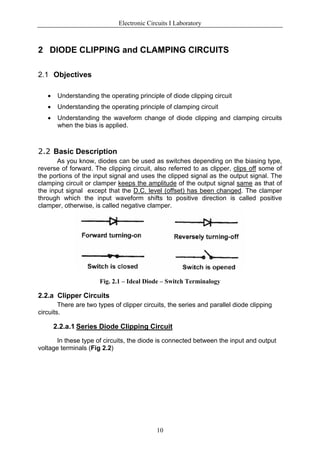
  • 1. Electronic Circuits I Laboratory 2 DIODE CLIPPING and CLAMPING CIRCUITS 2.1 Objectives • Understanding the operating principle of diode clipping circuit • Understanding the operating principle of clamping circuit • Understanding the waveform change of diode clipping and clamping circuits when the bias is applied. 2.2 Basic Description As you know, diodes can be used as switches depending on the biasing type, reverse of forward. The clipping circuit, also referred to as clipper, clips off some of the portions of the input signal and uses the clipped signal as the output signal. The clamping circuit or clamper keeps the amplitude of the output signal same as that of the input signal except that the D.C. level (offset) has been changed. The clamper through which the input waveform shifts to positive direction is called positive clamper, otherwise, is called negative clamper. Fig. 2.1 – Ideal Diode – Switch Terminalogy 2.2.a Clipper Circuits There are two types of clipper circuits, the series and parallel diode clipping circuits. 2.2.a.1 Series Diode Clipping Circuit In these type of circuits, the diode is connected between the input and output voltage terminals (Fig 2.2) 10
  • 2. Electronic Circuits I Laboratory Fig. 2.2 As Fig.2.2 reveals, the negative cycle of the input voltage can be clipped of by this type of series clippers. Reverse of the diode pins yields to a positive cycle clipping circuit as shown in Fig. 2.3. Fig. 2.3 Previous circuits clip the values larger or smaller than zero voltage. This voltage, technically called “threshold voltage” and can be changed to a desired value by inserting a D.C. voltage source. This is achieved in two different ways. In the first type, the voltage source of Em ( positive or negative) is connected through output terminals as in Fig. 2.4. Depending on the diode connection (normal 11
  • 3. Electronic Circuits I Laboratory or reverse), the values smaller (Fig.2.4.a) or greater (Fig.2.4.b) than Em is clipped and assigned as Em. . a b Fig. 2.4. Note that if Em is negative, ( where the voltage source is reversely connected) again the values smaller or larger than this negative value is clipped, do not get confused. In the second type of thresholded series clipping, the voltage source is applied between the input and output terminals, series with the diode. This time, the clipped values are assigned to zero and the net output voltage equals to the difference between the input and threshold values.(If Em is negative, then E0 = E – Em = E + |Em|) a b Fig. 2.5 12
  • 4. Electronic Circuits I Laboratory 2.2.a.2 Parallel Diode Clipping Circuit In this type of clippers, the diode is connected between output terminals. The on/off state of diode directly affects the output voltage. These type of clippers may also have a non-zero threshold voltage by addition of a voltage series with diode. Following figures illustrate the clipping process. a b Fig. 2.6 – Zero Threshold Parallel Clippers a b Fig. 2.7 – Thresholded Parallel Clippers 13
  • 5. Electronic Circuits I Laboratory 2.2.b Clamper Circuits Clamper Circuits, or briefly clampers are used to change the D.C. level of a signal to a desired value.( Fig 2.8 ). Fig 2.8 Being different from clippers, clamping circuits uses a capacitor and a diode connection. When diode is in its on state, the output voltage equals to diode drop voltage (ideally zero) plus the voltage source, if any. Now let us examine the clamping process for the circuit in Fig. 2.9. Fig 2.9 – Typical Clamping Circuit As you know, this circuit, in fact, is a series R-C circuit. The resistance of diode ( several ohms above its drop voltage) and the small capacitance yield to a small time-constant for this circuit. This means that the capacitor will rapidly be charged if any input voltage, that is enough to swtich on the diode, is applied. The diode will conduct during the positive cycle of the input signal (Fig. 2.10) and output voltage will be ideally zero ( in practice this voltage equals ~0.6 V). Fig 2.10. Diode conducts during positive cycle Note that during positive cycle the capacitor is rapidly charged in inverse polarity with the input voltage. After transition to negative cycle, the diode becomes to its off state. In this case, the output voltage equals to the sum of the input voltage and the voltage across the terminals of the capacitor which have the same polarity with each other.(Fig 2.11) 14
  • 6. Electronic Circuits I Laboratory E0 = - ( |Ei |+ |Ec | ) Fig. 2.11. Diode is switched off during negative cycle The resulting signal after a complete cycle is shown below. Fig. 2.12 By this process, the input signal is shifted to negative D.C. value (its maximum value is ideally zero) without any change in its amplitude ideally. There exist again modified versions of this circuit inwhich a threshold value is inserted for clamping. Following figures illustrate these modifications and resulting outputs. 15
  • 7. Electronic Circuits I Laboratory Fig.2.13 Fig. 2.14 16
  • 8. Electronic Circuits I Laboratory 2.3 Experiment Equipments 1. KL- 200 Linear Circuit Lab. Device 2. Experiment Module: KL-23001 3. Experiment Instruments: Oscilloscope, Multimeter 4. Connection cables and short-circuit clips 2.4 Procedures Procedure 1: Series Diode Clipping Circuit (1) Locate block b of module KL-23001 (2) Insert short-circuit clips refering to Fig. 2.15 a Fig. 2.15 (3) Using oscilloscope, adjust function generator to 10 V p-p ( 7.07 V rms) , 1kHz Sine wave. Make a good adjustment since this signal is the common input signal that will be used during whole experiment. (4) Adjust oscilloscope divisions until you have a clear view of input signal. 17
  • 9. Electronic Circuits I Laboratory (5) Disconnect function generator output from oscilloscope and apply this to TP2. (6) Examine the output signal by connecting the second channel of oscilloscope to TP3. Record the plot on Graph 2.1 a. (7) Turn off all active devices, and reconfigure the short-circuit clips refering to Fig. 2.15 b. (8) Only change the generator output from TP2 to TP1. (9) Again examine the output waveform and plot output waveform on Graph 2.1.b a b Graph 2.1 18
  • 10. Electronic Circuits I Laboratory Procedure 2: Thresholded Series Diode Clipping Circuit In this procedure, a threshold value is added to the previous circuit layout. This is achieved by substitution of lower short-circuit clip with a voltage source. (1) Turn off all active devices, and connect short-circuit clip and voltage source ( + 5 V DC) by refering to Fig.2.16-a. Fig. 2.16 (2) Record the plot of output voltage on Graph 2.2.a (on Pg. 25) (3) Turn off all active devices, and reconfigure short-circuit clips refering to Fig.2.16-b. (4) Plot output waveform on Graph 2.2.b Turn off all active devices. Now you will apply negative threshold value to the clipper circuit. (5) Refering to Fig.2.17-a, reconfigure short circuit clips and substitute +5V DC source with -5 V DC Source. Do not directly reverse the terminals of + 5 V source, this will cause a short circuit !!! 19
  • 11. Electronic Circuits I Laboratory Fig. 2.17 (6) Observe and plot the output waveform on Graph 2.2.c (7) Turn off all active devices again and rearrange short circuit clip refering to Fig.2.17.b (8) Observe and plot output voltage on Graph 2.2.d 20
  • 12. Electronic Circuits I Laboratory a b c d Graph 2.2 Procedure 3: Parallel Diode Clipping Circuit (1) Locate block c of module KL-23001 (2) Refer to Fig.2.18-a and arrange short circuit clips. 21
  • 13. Electronic Circuits I Laboratory a b Fig. 2.18 (3) Observe output voltage on TP2 and plot on Graph 2.3.a (4) Turn off all active devices and rearrange short circuit clips by refering to Fig. 2.18 b. (5) Observe output voltage on TP2 and plot on Graph 2.3.b a b Graph 2.3 22
  • 14. Electronic Circuits I Laboratory Procedure 4 : Diode Clamping Circuit (1) Now locate block e. (2) Arrange clips according to Fig.2.19-a. a b Fig. 2.19 (3) Observe and plot OUT voltage on Graph 2.4.a (4) Turn off all active devices and rearrange circuit in Fig. 2.19-b (5) Again plot OUT voltage on Graph 2.4.b. 23
  • 15. Electronic Circuits I Laboratory a b Graph 2.4 2.5 Conclusion In this experiment you have learned two main types of diode circuits. • Clippers • Clampers Although the clippers are also classified into series and parallel clipping circuits, both circuits are based on the same principle. In other words, the design of both circuits utilizes the characteristics of diode that will be forward turned on and will reversely turned off. Clampers can be used to change the DC level of an input signal. 24