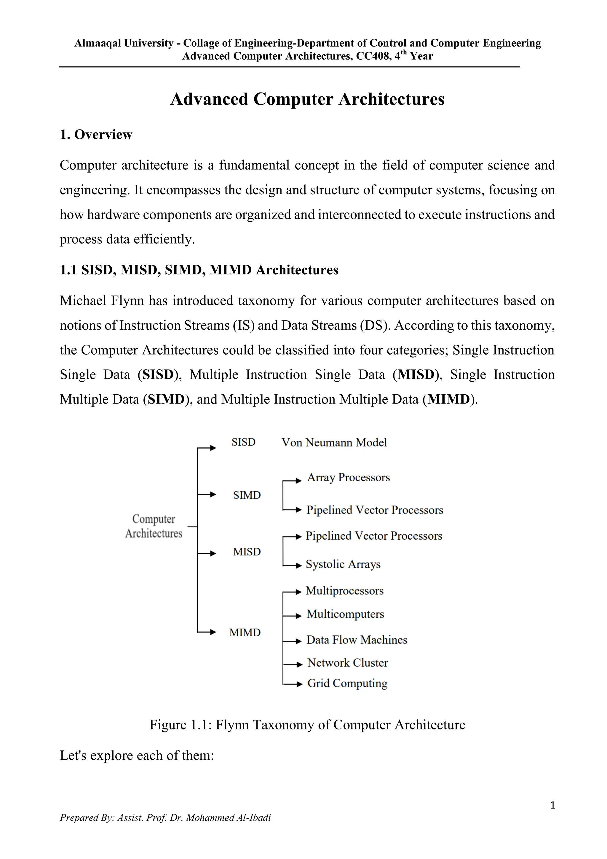
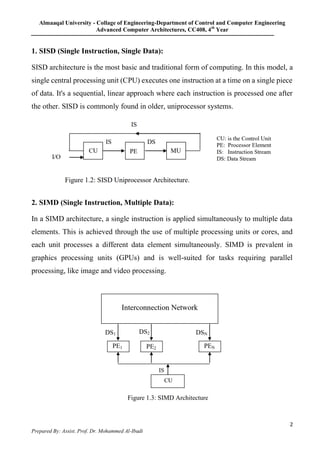
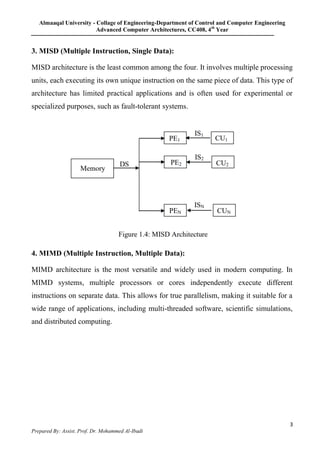
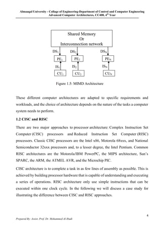
1. The document discusses different computer architectures according to Michael Flynn's taxonomy: SISD, SIMD, MISD, and MIMD. It provides examples of each type and explains their characteristics.
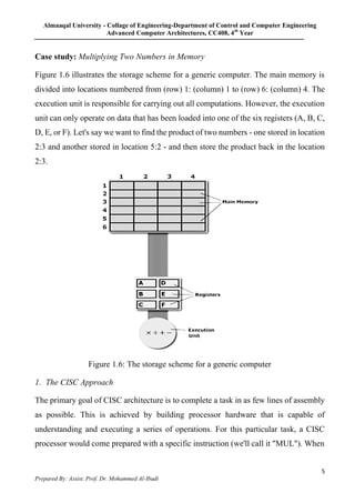
2. CISC and RISC architectures are explored through a case study of multiplying two numbers. CISC uses complex instructions to perform the calculation in one step, while RISC separates it into load, calculate, and store simple instructions.
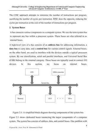
3. The tradeoffs between CISC and RISC are summarized. CISC minimizes instructions while increasing cycles per instruction, while RISC does the opposite to optimize for speed and power efficiency. The document also briefly mentions system buses.