This document contains an assignment submission for a course on VLSI Design. It includes:
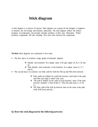
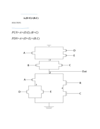
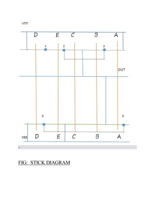
1) An explanation of stick diagrams and how they are constructed to visualize transistor placement and routing for a logic circuit.
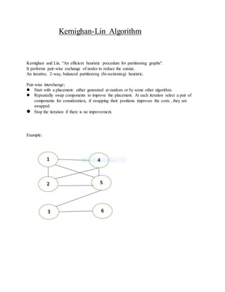
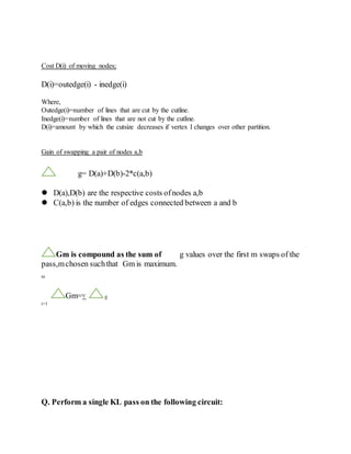
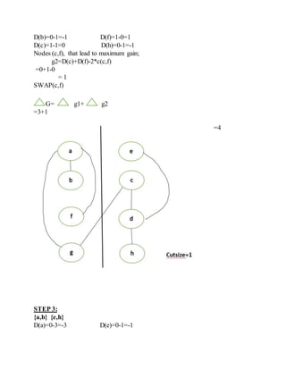
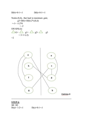
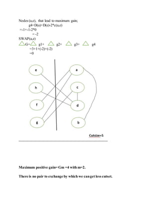
2) An overview of the Kernighan-Lin algorithm for iterative partitioning of graphs to minimize cut size through pairwise exchange of nodes between partitions.
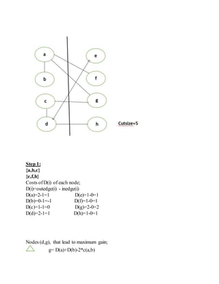
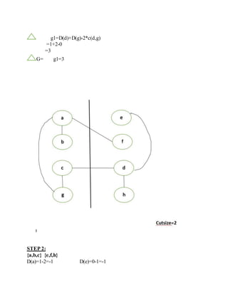
3) An example application of a single pass of the Kernighan-Lin algorithm on a sample circuit to demonstrate the process.


![[DSC Europe 25] Ekaterina Bubenko - Behind the Curtain: How Data Roles Collab...](https://cdn.slidesharecdn.com/ss_thumbnails/anmv6x8dstqbbzchoklr-ekaterina-bubenko-behind-the-curtain-how-data-roles-collaborate-in-the-ai-era-a-260123083019-4b252ec7-thumbnail.jpg?width=640&height=640&fit=bounds)


![[DSC Europe 25] Josip Saban - Career building for data professionals.pptx](https://cdn.slidesharecdn.com/ss_thumbnails/zroflcttkm1vmli0txea-josip-saban-career-building-for-data-professionals-260123083019-587cdb8c-thumbnail.jpg?width=640&height=640&fit=bounds)


