Download to read offline

![K. Yamuna, C. Chandrasekhar / International Journal of Engineering Research and
Applications (IJERA) ISSN: 2248-9622 www.ijera.com
Vol. 3, Issue 4, Jul-Aug 2013, pp.1772-1777
1773 | P a g e
Several architectures like direct mapped, folded, and
flipping for single level and multi-level DWT have
been proposed to implement 1-D lifting DWT. Much
architecture that implement the Two-Dimensional
separable Forward (2D-DWT) and Inverse DWT
(2D-IDWT) in order to be applied on 2D signals have
been presented in the past. These architectures are
consisting of filters for performing the 1D-DWT and
memory units for storing the results of the
transformation. Due to the fact that streaming
multimedia applications - in which the DWT is
present - are characterized by high throughput
requirements, this imposes the need for optimizing
the design of the filters in terms of speed. Moreover,
portable multimedia devices require low power
consumption for increasing the battery lifetime and
this can be achieved by minimizing the storage size
and number of memory accesses. Low power DWT
architectures based on pipelining and parallel
processing has been discussed, in their work low
power is achieved by modifying the architecture to
reduce number of computations the design was
implemented on FPGA. Many of the low power
techniques reported for DWT propose modifications
in the architecture level to reduce power dissipation.
Power reduction can be accomplished at various
levels of abstraction starting from architecture level
to circuit level. Power reduction at the sub system
level or at the circuit level can be accomplished when
ASIC design of DWT architecture is performed.
Many of the work reported in literature have
restricted to FPGA implementation. In this paper, in
order to demonstrate the dynamic power reduction
techniques at various levels of abstraction, DWT
architecture is considered as a test case for
illustration. ASIC design of DWT architecture
optimizing dynamic power reduction using 65nm
TSMC libraries is performed
II. WALLACE TREE MULTIPLIER
A Wallace tree is an efficient hardware
implementation of a digital circuit that multiplies two
integers. The benefit of the Wallace tree is that there
are only reduction layers, and each layer
has propagation delay. As making the partial
products is and the final addition is
, the multiplication is only ,
not much slower than addition (however, much more
expensive in the gate count). Naively adding partial
products with regular adders would require
time. From a complexity theoretic
perspective, the Wallace tree algorithm puts
multiplication in the class NC1.
These computations only consider gate delays and
don't deal with wire delays, which can also be very
substantial.
Fig.1.Wallace tree multiplier
The Wallace tree can be also represented by
a tree of 3/2 or 4/2 adders. It is sometimes combined
with Booth encoding.
III. LIFTING SCHEME
The Lifting Scheme is a well-known method
for constructing bi-orthogonal wavelets. The main
difference with the classical construction is that it
does not rely on the Fourier transform. The lifting
scheme is an efficient implementation of a wavelet
transform algorithm. It was primarily developed as a
method to improve wavelet transform, and then it
was extended to a generic method to create so-called
second-generation wavelets. Second-generation
wavelets are much more flexible and powerful than
the first generation wavelets. The lifting scheme is an
implementation of the filtering operations at each
level [6]. The figure 3 represents the classical and
lifting based implementations of DWT.
Fig.2.Lifting scheme
Lifting Scheme consists of three steps:
SPLIT, PREDICT and UPDATE, as shown in the
figure 2.
SPLIT: In this step, the data is divided into ODD
and EVEN elements.
PREDICT: The PREDICT step uses a function that
approximates the data set. The differences between
the approximation and the actual data, replace the
odd elements of the data set. The even elements are
left unchanged and become the input for the next step
in the transform. The PREDICT step, where the odd](https://image.slidesharecdn.com/ju3417721777-130813005249-phpapp01/85/Ju3417721777-2-320.jpg)
![K. Yamuna, C. Chandrasekhar / International Journal of Engineering Research and
Applications (IJERA) ISSN: 2248-9622 www.ijera.com
Vol. 3, Issue 4, Jul-Aug 2013, pp.1772-1777
1774 | P a g e
value is "predicted" from the even value is described
by the equation
Oddj+1, i = oddj, i – P (evenj, i)
UPDATE: The UPDATE step replaces the even
elements with an average. These results in a smoother
input for the next step of the wavelet transform. The
odd elements also represent an approximation of the
original data set, which allows filters to be
constructed. The UPDATE phase follows the
PREDICT phase. The original values of the odd
elements have been overwritten by the difference
between the odd element and its even "predictor". So
in calculating an average the UPDATE phase must
operate on the differences that are stored in the odd
elements:
Evenj+1, i = evenj, i + U (oddj+1, i)
The equations for the lifting based implementation of
the bi-orthogonal wavelet are:
Predict P1: di1 = α (x2i + x2i+2) +x2i+1 .. (1)
Update U1: ai1 = β (di1+di-11) + x2i ….. (2)
Predict P2: di2 = γ (ai1 + ai+1) +x2i+1 …..(3)
Update U2: ai2 = δ (di2+di-12) + ai1 .. (4)
Scale G1: ai = ζ ai2 …... ( 5)
Scale G1: di = di2/ζ …….. (6)
The figure 4 shows the lifting scheme
architecture to realize the equations shown above.
Fig.3.Lifting Scheme Architecture
The input data x is first split into even and
odd samples and each of the samples are taken
through predict and update stages as per the
architecture shown above. As the data moves from
first stage to the last stage, data switching occurs at
the input and output of every stage. Every stage
consists of multipliers and adders. For the given set
of Predict and Update stages, assuming the value of i
= 0, the equation can be finalized.
IV. MODIFIED LIFTING SCHEME
By re-arranging all the values and the
constant co-efficient, the final equation can be
derived.
ai= (3 * γ.β.δ.ζ + δ.ζ + β.ζ ) [ α ( x0 + x2) + x1 + α (
x0 + x-2) + x-1] + ζ.δ.β.γ [α(x2 + x4) + x3 + α( x-2 +
x-4) + x-3] + ζ.δ.γ ( x0 + x2 + x0 + x-2) + ζ * x0
…… (7)
di= 1/ζ [(2 * γ.β +1){ α ( x0 + x2) + x1} + γ.β { α (
x0 + x-2) + x-1 + α(x2 + x4) + x3} +γ( x0 + x2)]
…...(8)
Being a dedicated DWT core for JPEG
2000, the filter coefficients are fixed. The filter
coefficients are: α = 1.586134342, β =
0.05298011854, γ = 0.8829110762, δ
=0.4435068522, ζ = 1.149604398. By substituting the
above values in the modified equation, the coefficient
values obtained then are also decimals, by
multiplying them with constants they form integers
as: 1 * 32 = 57, 2 * 256 = 6, 3 * 64 = 30, 4 * 32 = 35,
5 * 256 = 12, 6 * 32 = 26, 7 * 32 = 50.
Thus the above integers are the values of the
underlined coefficients in above equations. From the
equations it is observed that there are common lifting
coefficients to compute ai and di coefficients and
there are input terms. The architecture realised by the
above equations considering the constant coefficients
is shown in the figure 4.
Figure 4 Modified Lifting Scheme Architecture for
DWT
Table 1 Estimation of Power, Delay and Area of sub
blocks](https://image.slidesharecdn.com/ju3417721777-130813005249-phpapp01/85/Ju3417721777-3-320.jpg)
![K. Yamuna, C. Chandrasekhar / International Journal of Engineering Research and
Applications (IJERA) ISSN: 2248-9622 www.ijera.com
Vol. 3, Issue 4, Jul-Aug 2013, pp.1772-1777
1776 | P a g e
accepts any number of bitstream and creates one or
more PROM files containing one or more daisy chain
configuration
Fig.7.simulation results for the DWT Architecture
TABLE 2 Synthesis results of modified lifting based
DWT
Parameters Lifting
based DWT
Modified
Lifting based
DWT with
low power
Area(sq.
mm)(LUT’s)
2179(7%) 835(3%)
Power(W) 0.103 0.103
Operating
frequency(max)
MHz
151.814 520.738
VI. CONCLUSION
In this work a modified lifting based DWT
architecture is proposed, designed, modeled and
verified. The design is modeled using HDL and is
implemented on FPGA. The interfaces required for
data processing are also designed and is used to
synchronize the data transfer operation. The HDL
models and simulation of the sub blocks have been
done to model the top-level design architecture. The
test-bench to verify the functionality and
performance of the sub modules and the top level
architecture have been done. Implemented the design
on FPGA and verified and debugged through the
Chip-Scope. The Pre and Post Synthesis have been
done and compared. The design can be further
optimized for video signal processing.
REFERENCES
[1] N. Jayant and P. Noll, Digital Coding of
Waveforms: Principles and Applications to
Speech and Video. Englewood Cliffs, NJ:
Prentice-Hall, 1984.
[2] C. Diou, L. Torres, and M. Robert, “A
wavelet core for video processing,”
presented at the IEEE Int. Conf. Image
Process., Sept. 2000.
[3] N. Jayant, J. Johnston, and R. Safranek,
“Signal compression based on models of
human perception,” Proc. IEEE, vol. 81, pp.
1385–1422, Oct. 1993.
[4] B. Zovko-Cihlar, S. Grgic, and D. Modric,
“Coding techniques in multimedia
communications,” in Proc. 2nd Int.
Workshop Image and Signal Processing,
IWISP’95, Budapest, Hungary, 1995, pp.
24–32.
[5] Digital Compression and Coding of
Continuous Tone Still Images, ISO/IEC IS
10918, 1991.
[6] I. Daubechies, Ten Lectures on Wavelets.
Philadelphia, PA: SIAM, 1992.
[7] S. Mallat, “A theory of multiresolutio
[8] n signal decomposition: The wavelet
representation,” IEEE Trans. Pattern Anal.
Machine Intell., vol. 11, pp. 674–693, July
1989.
[9] M. Nagabushanam, Cyril Prasanna Raj P, S.
Ramachandran, Design and Implementation
of Parallel and Pipelined Distributive
Arithmetic Based Discrete Wavelet
Transform IP Core, European Journal of
Scientific Research ISSN 1450-216X Vol.35
No.3 (2009), pp.378-392.
[10] M. Vishwanath, R. Owens, and M. J. Irwin,
“VLSI architectures for the discrete wavelet
transform,” IEEE Trans. Circuits Syst. II,
vol. 42, pp. 305–316, May 1995.
[11] J. S. Fridman and E. S. Manolakos,
“Discrete wavelet transform: Data
dependence analysis and synthesis of
distributed memory and control array.](https://image.slidesharecdn.com/ju3417721777-130813005249-phpapp01/85/Ju3417721777-5-320.jpg)


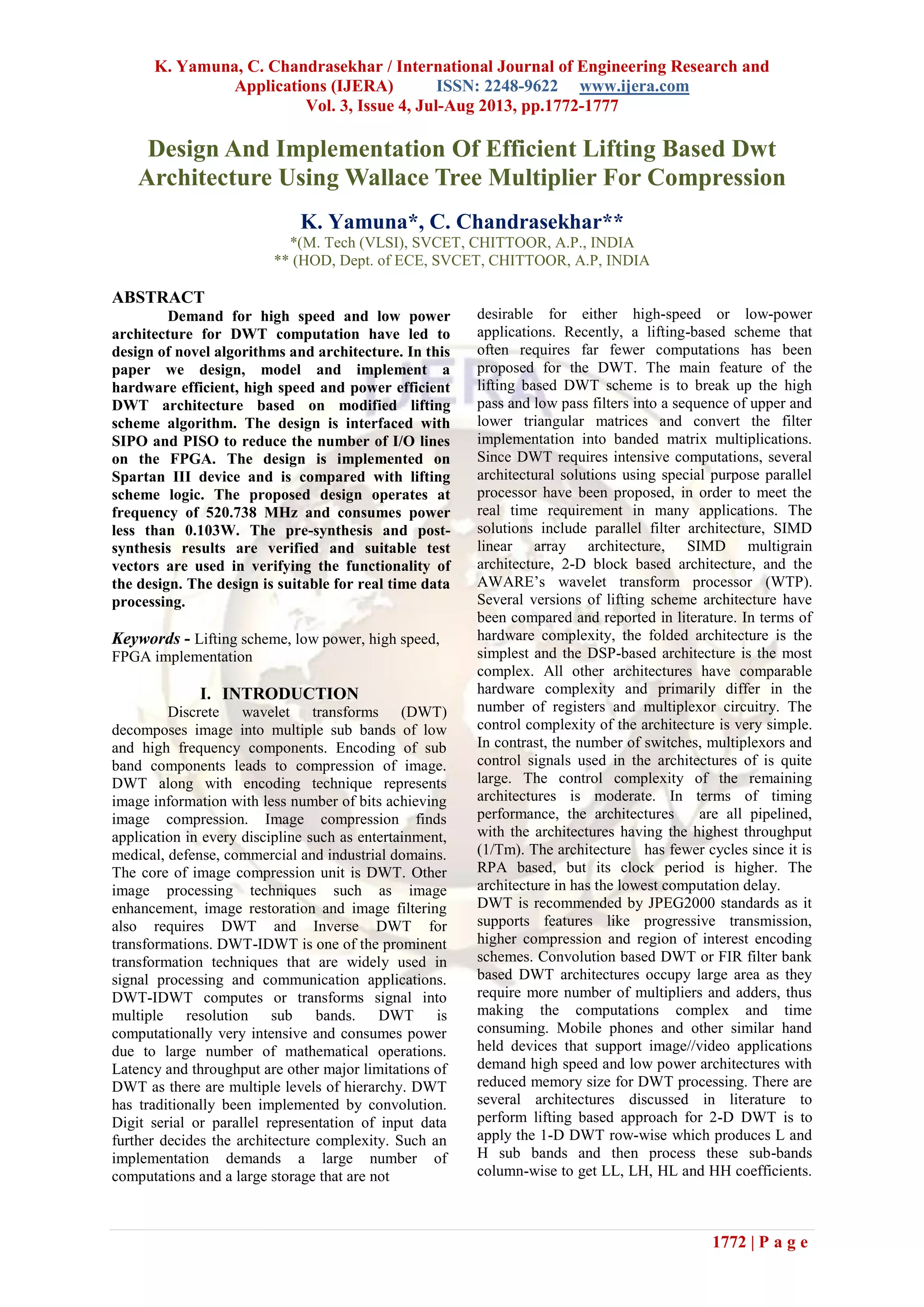
This paper presents a hardware-efficient discrete wavelet transform (DWT) architecture using a modified lifting scheme and Wallace tree multiplier for low power and high-speed operations, implemented on an FPGA device. The design achieved operational frequencies of 520.738 MHz with power consumption below 0.103W, making it suitable for real-time data processing applications. Various architectural solutions for DWT are compared, highlighting the proposed architecture's advantages in performance and reduced computational complexity.


![Getting Started with Apache Spark: Big Data Made Simple [Free Meetup]](https://cdn.slidesharecdn.com/ss_thumbnails/apachesparkgettingstarted-260203175547-8361bcc3-thumbnail.jpg?width=640&height=640&fit=bounds)


