Download as PDF, PPTX

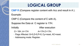

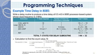
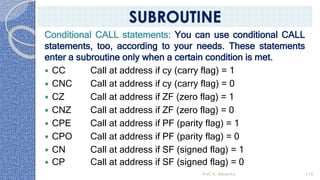
![➢ Here value of M= 17, N= 14.
➢ The maximum delay will occur if count is 255 or FF H.
➢ Thus Td max =17+[255x14]-3= 3584 T states.
➢ For 0.5 µsec delay for a T state, we get
➢ Td max=0.5 µsec x 3584= 1792 µsec or 1.792 m sec.
Prof. K. Adisesha 100
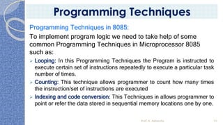
Programming Techniques](https://image.slidesharecdn.com/introductionto8085byadippt-221111162935-fee3312f/85/Introduction-to-8085-by-Adi-PPT-pdf-100-320.jpg)


This document provides an introduction to the 8085 microprocessor. It begins with defining microprocessors and their basic components like the ALU, control unit, and registers. It then describes the specific architecture of the 8085, including that it is an 8-bit processor that can access 64KB of memory. The document outlines the instruction set and addressing modes of the 8085 as well as its interrupts and peripheral interfacing. It provides details on the internal registers, timing and control, and machine cycles of the 8085. Finally, it discusses the instruction cycle and classifications of 8085 instructions based on size and function.