Download to read offline
![International Journal of VLSI design & Communication Systems (VLSICS) Vol.4, No.1, February 2013
DOI : 10.5121/vlsic.2013.4108 93
IMPLEMENTATION OF COMPACTION
ALGORITHM FOR ATPG GENERATED
PARTIALLY SPECIFIED TEST DATA
Vaishali Dhare1
and Dr. Usha Mehta2
1
Assistant Professor, Institute of Technology, Nirma University, Ahmedabad
2
Senior Associate Professor, Institute of Technology,
Nirma University, Ahmedabad
1
vaishalidhare@nirmauni.ac.in 2
usha.mehta@nirmauni.ac.in
ABSTRACT :
In this paper the ATPG is implemented using C++. This ATPG is based on fault equivalence concept in
which the number of faults gets reduced before compaction method. This ATPG uses the line justification
and error propagation to find the test vectors for reduced fault set with the aid of controllability and
observability. Single stuck at fault model is considered. The programs are developed for fault equivalence
method, controllability Observability, automatic test pattern generation and test data compaction using
object oriented language C++. ISCAS 85 C17 circuit was used for analysis purpose along with other
circuits. Standard ISCAS (International Symposium on Circuits And Systems) netlist format was used. The
flow charts and results for ISCAS 85 C17 circuits along with other netlists are given in this paper. The test
vectors generated by the ATPG further compacted to reduce the test vector data. The algorithm is
developed for the test vector compaction and discussed along with results.
KEYWORDS :
Test vector, compaction, ISCAS, ATPG.
1. INTRODUCTION
Test vector size is the big issue in the today’s technology. As size of circuit increases the size of
test vector also increases so that the memory. This paper includes such ATPG which itself
compacts test patterns before further compression of the test patterns. ATPG (acronym for both
Automatic Test Pattern Generation and Automatic Test Pattern Generator) is an electronic design
automation method/technology used to find an input (or test) sequence that, when applied to a
digital circuit, enables testers to distinguish between the correct circuit behavior and the faulty
circuit behavior caused by defects[1]. The generated patterns are used to test semiconductor
devices after manufacture, and in some cases to assist with determining the cause of failure
(failure analysis) the effectiveness of ATPG is measured by the amount of modeled defects, or
fault models, that are detected and the number of generated patterns. These metrics generally](https://image.slidesharecdn.com/4113vlsics08-190520090056/85/IMPLEMENTATION-OF-COMPACTION-ALGORITHM-FOR-ATPG-GENERATED-PARTIALLY-SPECIFIED-TEST-DATA-1-320.jpg)
![International Journal of VLSI design & Communication Systems (VLSICS) Vol.4, No.1, February 2013
94
indicate test quality (higher with more fault detections) and test application time (higher with
more patterns). ATPG efficiency is another important consideration. It is influenced by the fault
model under consideration, the type of circuit under test (full scan, synchronous sequential, or
asynchronous sequential), the level of abstraction used to represent the circuit under test (gate,
register-transistor, switch), and the required test quality [2].
The single stuck-at-fault model has been widely accepted as a standard target model to generate a
set of test patterns to detect all the stuck faults in the circuit. A single stuck-at fault represents a
line in the circuit that is fixed to logic value 0 or 1. The single-stuck fault model is also referred to
as the classical or standard fault model because it has been the first and the most widely studied
and used. Although its validity is not universal, its usefulness results from the following
attributes:
The single stuck at fault can be used to represent short or open ,caused due to short between
ground or power line, causing a signal line remain at a fixed voltage level.If we consider single
stuck at fault then the number of faults is 2n, where n is number of net .In this case we have to
find 2n test vectors, for each fault (stuck at 0, stuck at 1) on each net. Size of test vector
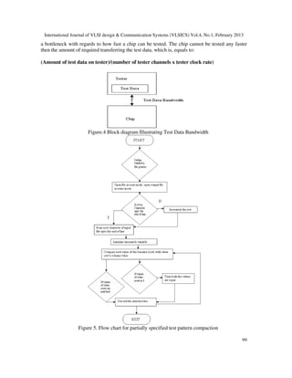
becomes large for large combinational circuits. ATE (Automatic Test Equipment) bandwidth
problem cause to handle these test vectors and testing time may be more in this case. No doubt
test vector compression methods are available, prior to that, befor test generation the number of
faults can be reduced sothat the test vectors. The number of faults can be reduced using fault
equivalence method and fault dominance method. In this paper an attempt is made to reduce the
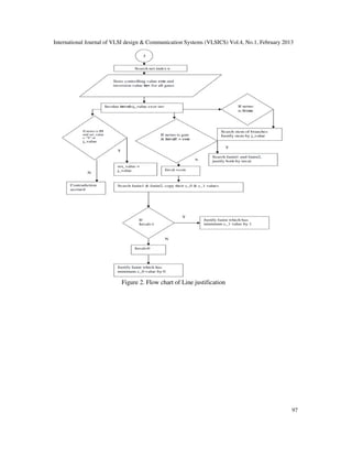
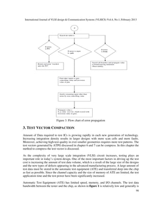
fault set using fault equivalence method and developed in C++. The logic and flow chart of the
program are given in this paper. The results for ISCAS C17 benchmark circuit were analyzed.
The generated test pattern for ISCAS C17 circuit is discussed in result section .The logic and flow
chart is discussed in this paper. The test pattern compaction algorithm is discussed along with the
results and comparisons.
.
2. ATPG
A defect is an error introduced into a device during the manufacturing process. A fault model is a
mathematical description of how a defect alters design behavior. A fault is said to be detected
by a test pattern if, when applying the pattern to the design, any logic value observed at one or
more of the circuit's primary outputs differs between the original design and the design with the
fault. The ATPG process for a targeted fault consists of two phases: fault activation and fault
propagation. Fault activation establishes a signal value at the fault model site that is opposite of
the value produced by the fault model. Fault propagation moves the resulting signal value, or
fault effect, forward by sensitizing a path from the fault site to a primary output [9].
The ATPG process for a targeted fault consists of two phases: fault activation and fault
propagation. Fault activation establishes a signal value at the fault model site that is opposite of
the value produced by the fault model. Fault propagation moves the resulting signal value, or
fault effect, forward by sensitizing a path from the fault site to a primary output.](https://image.slidesharecdn.com/4113vlsics08-190520090056/85/IMPLEMENTATION-OF-COMPACTION-ALGORITHM-FOR-ATPG-GENERATED-PARTIALLY-SPECIFIED-TEST-DATA-2-320.jpg)
![International Journal of VLSI design & Communication Systems (VLSICS) Vol.4, No.1, February 2013
103
REFERENCES
[1] D. Whitley Sokolov, A. Sanyal and Y. Malaiya. Dynamic power minimization during combinational
circuit test as a travelling salesman problem. In the proceeding of the IEEE Congress on Evolutionary
Computation, vol.2, pp. 1088-1095,Sept 2005.
[2] Jennifer Dworak, Michael R. Grimaila, Sooryong Lee, Brad Cobb and M. Ray Mercer. A new atpg
algorithm to limit test set size and achieve multiple detections of all faults. In the proceedings of
Design, Automation and Test, Europe, 2002.
[3] Nur A. Touba. Survey of Test vector Compression Techniques. In the IEEE Design and Test of
Computers, July-August 2006.
[4] S.C. Seth, L. Pan and V.D Agrawal, PREDICT: Probabilistic Estimation of Digital Circuit Testability.
In the Proceedings of Fault Tolerant Computing System, pp. 220-225, 1985.
[5] S.C. Chang, W.B. Jone and SS. Chang. TAIR: Testability Analysis by Implication Reasoning. In the
IEEE Transaction on CAD, Volume 19, No. 1, pp. 152-160, January 2000.
[6] L.H. Goldstein. Controllability/Observability Analysis of digital circuits. In the IEEE Transactions on
Circuits and Systems, Vol. 26, pp. 685-693, September 1984.
[7] David Bryan. ISCAS’85 benchmark circuits and netlist format. North Carolina State University.
[8] M. Abramovici and R. Aitken. Error, Fault and Defect Diagnosis: A Detective Story. Tutorial, IEEE
International Test Conference, 1997.
[9] Abramovici, Melvin A. Breuer, and Arthur D. Friedman. Digital Systems Testing and Testable
Design. Jaico Publication.
[10] Michael Bushnell and Vishwani Agrawal. Essentials of Electronic Testing. Springer Publication.
[11] Xiaoqing Wen Laung Terng Wang, Cheng Wen Wu. VLSI Test Principles and Architectures. Morgan
Kaufmann, 2006.
[12] Vaishali H. Dhare, Usha Mehta, “Object Oriented Implementation of Combinational Controllability
and Observability Algorithms”, International Journal on Electronics Engineering: Kurukshetra,
Hariyana Volume2, Number-1, June 2010, Pg.No 93-97.
[13] Vaishali H. Dhare, Usha Mehta, “Development of Controllability Observability Aided Combinational
ATPG with Fault Reduction”, First International Workshop on VLSI Design 2010 , Chennai ,
July2010, Pg. No 682-692](https://image.slidesharecdn.com/4113vlsics08-190520090056/85/IMPLEMENTATION-OF-COMPACTION-ALGORITHM-FOR-ATPG-GENERATED-PARTIALLY-SPECIFIED-TEST-DATA-11-320.jpg)

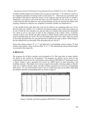
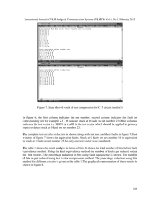
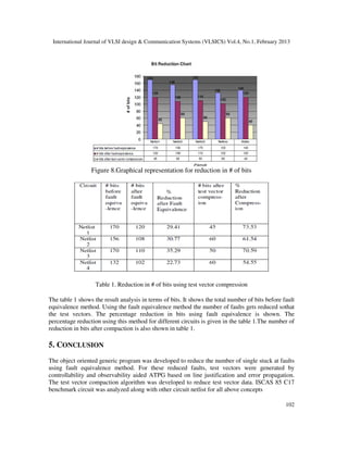
This paper presents a method for implementing an Automatic Test Pattern Generation (ATPG) algorithm using C++ that reduces the number of faults and compacts test vectors for VLSI circuits. It describes the application of fault equivalence and test vector compaction techniques to streamline the testing process, particularly referencing the ISCAS 85 C17 benchmark circuit. The study concludes that the developed generic programs effectively reduce the size of test vectors while maintaining test quality.