HPC Impact: EDA Telemetry Neural Networks
•
0 likes•313 views

The document discusses using systems intelligence and artificial intelligence/neural networks to enhance semiconductor electronic design automation (EDA) workflows by collecting telemetry data from EDA jobs and infrastructure and analyzing it using complex event processing, machine learning models, and messaging substrates to provide insights that could optimize EDA pipelines and infrastructure. The approach aims to allow both internal and external augmentation of EDA processes and environments through unsupervised and incremental learning.

Recommended
Recommended
More Related Content
What's hot
What's hot (20)
Similar to HPC Impact: EDA Telemetry Neural Networks
Similar to HPC Impact: EDA Telemetry Neural Networks (20)
More from inside-BigData.com
More from inside-BigData.com (20)
Recently uploaded
Recently uploaded (20)
HPC Impact: EDA Telemetry Neural Networks
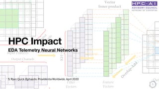
- 1. Providentia Worldwide S. Ryan Quick @phaedo, Providentia Worldwide. April 2020 HPC Impact EDA Telemetry Neural Networks
- 3. Providentia Worldwide Systems Intelligence Principles Methodology for leveraging multiple data domains through complex data processing Disparate / Unlike Domains Messaging Middleware Insight Insight
- 4. Providentia Worldwide • Aggregation • Event Statistics • Atomic Pattern Recognition • Simple example shown as “waterfalling” for illustration — the operations are parallel and stateless • Pattern is an example of the type and method of telemetry we use for EDA environmental and in-workload collection to feed AI and neural networks inline • There are literally thousands of metrics for a single operation, millions per job Multiple-Domain Simple Data Access Metrics Calculator CPU Event Source app login r/sec app successful login r/sec app failed login r/sec cpu 1m load avg cpu 5m load avg cpu 15m load avg cpu blocked proc cnt cpu running proc cnt cpu waiting proc cnt cpu user % cpu idle % cpu system % cpu io wait % db active queries db slow queries db selects db updates db deletes db rows fetched db table locks held db row locks held Available Source Fields App Login Event Source DB Access Event Source > 3? app failed login / app success login * 100 AVG(cpu waiting / cpu running)) / cpu 1M load avg * 100 > 0.5? DB Slow Queries > 4? Anomaly Detected: Potential Login Attack yes yes yes
- 5. Providentia Worldwide • Affinity + Simple Case • Stream + Augmented Datasource • Parallel Stream • Frequency-Shifted Stream • “Correlative/Normalized View”: Similar to a SQL “join” concept, we relate data fields in disparate stream sources • Many examples — for other talks :) • This illustrates the mechanisms by which we can combine and augment data types for complex events in AI/neural networks and utilize inline training and active models. • Also allows us to introduce the notion of insight, which is crucial to incremental improvement model — especially for “slight touch ecosystems” like coral reefs Multiple-Domain Complex Event Processing Approaches Complex Event Processor CPU Source Zookeeper Source RabbitMQ Source Application Event Source Parallel Source Disparate Normalization Correlative/ Normalized View Correlative/ Normalized View Correlative/ Normalized View approx-data-sz avg-latency ephemeral-count followers max-fd-cnt max-latency min-latency open-fd-cnt num-alive-connections outstanding-requests packets-received packets-sent pending-syncs synced-followers watch-cnt znode-cnt Zookeeper message total message ready message unasked rate.publish rate.deliver rate.redeliver rate.confirm rate.ack connection.total connection.idle channel.total channel.publisher channel.consumer channel.duplex channel.inactive exchange.rate.phaedo q.total q.idle q.messages.phaedo q.consumers.phaedo q.memory.phaedo q.ingress.phaedo q.egress.phaedo binding.total RabbitMQ
- 6. Providentia Worldwide Semiconductor EDA Designing the Digital Future
- 7. Providentia Worldwide HPC HTC • “High Throughput Computing” • Very predictable, common engineering pipeline • Toolset geared to repeat the steps in the pattern 100s, 1000s of times per iteration, per engineer constantly. Each adjustment cascades hundreds/ thousands of small jobs. • Jobs are very short lived. Avg time on single core is under 3s. Job scheduler itself is often a bottleneck on large, shared systems. • EDA requires multiple phases of HDL synthesizers and HLL compilers and so can result in different sorts of computational bottlenecks at different phases of the pipeline as well as resulting for different design choices in the engineering decisions. EDA Characteristics
- 8. Providentia Worldwide Well-established Sector • Traditional enterprise storage (NFS3) • 10-100M small <=1M files/dir) • user and group based access controls • POSIX, locking not required • OS scheduler is often sufficient. Sometimes, job submission separated by login node. • License model well understood, and generally by core or time-based. Codes are generally proprietary. • Turnkey deployment is up and running in minutes on nearly any sized system. Very little motivation to alter the status quo. EDA Characteristics
- 9. Providentia Worldwide What Would it Take to Try something new? • All on-prem, w/ cloud tests successful but not adopted: • too costly • intellectual property concerns • ROI delayed • data management difficulties • Storage enhancements show improvements, and large shops adopt those, but NFS3 performs well for most small-medium practitioners. EDA Environments
- 10. Providentia Worldwide What Would it Take to Try something new? • EDA Process is well-known, easy-to- hire to, and well-understood in the industry. Why rock the boat? • Any perturbations to the system would need to overcome the cost of change, which in semiconductor fabrication can be immense. • Even where bottlenecks are known (storage, compute, scheduling), they are understood and manageable. New is new and unpredictable with unknown value… EDA Pipelines at Scale?
- 11. Providentia Worldwide For valuable and motivational change in semiconductor EDA, we need disruption both in behavior and environment simultaneously.
- 12. Providentia Worldwide External focus for HTC/Systems Intelligence • Two primary mechanisms for augmenting the EDA process: Internally (inside the EDA pipeline). Externally (augmenting and enhancing the pipelining environment). We are focusing here for this project, but the usual neural network caveats apply. Neural Networks for EDA Pipelines Semiconductor Electronic Design Automation «precondition» API to workflow data Chip Specification Design entry/Functional verification RTL synthesis Partitioning of chip Design for test (DFT) insertion Floor planning Placement stage Clock tree synthesis (CTS) Routing stage Final verification GDS II Infrastructure Automation «precondition» API to all components «precondition» API backwards compatible Systems Provisioning Network Provisioning Application Deployment Configuration Management Platform Management Change Orchestration capabilities XY User/group file CRUD Workflow scheduling Job management License management sd Systems Intelligence — EDA Messaging Substrate Data Analytics Command & Control Internal External
- 13. Providentia Worldwide Semiconductor EDA Designing the Digital Future “When we think of sensing technologies as devices that order the world, rather than devices that describe it, then alternative relationships between the social and the technical are strikingly brought to light.” — Genevieve Bell (Intel) @feraldata
- 14. Providentia Worldwide EDA Workflow and Supporting Infrastructure SI Messaging XY User/group file CRUD Workflow scheduling Job management License management X Y sd Systems Intelligence — EDA Messaging Substrate C E P I n g e s t Data Analytics inline models offline models Atomic Pattern Recognition Parallel Stream Command & Control Stream Augmentation data/scores/metrics decisioning orchestration validation feedback Frequency-Shifted Streams Affinity Streams Aggregation/ Statistics Semiconductor Electronic Design Automation «precondition» API to workflow data Chip Specification Design entry/Functional verification RTL synthesis Partitioning of chip Design for test (DFT) insertion Floor planning Placement stage Clock tree synthesis (CTS) Routing stage Final verification GDS II Infrastructure Automation «precondition» API to all components «precondition» API backwards compatible Systems Provisioning Network Provisioning Application Deployment Configuration Management Platform Management Change Orchestration capabilities XY User/group file CRUD Workflow scheduling Job management License management X Y sd Systems Intelligence — EDA Messaging Substrate C E P I n Data Analytics inline models offline models Atomic Pattern Recognition Command & Control Stream Augmentation data/scores/metrics decisioning orchestration External Capabilities and Infrastructure EDA SI Messaging Substrate Insight Insight
- 15. Providentia Worldwide EDA Workflow and AI/NN Frameworks Semiconductor Electronic Design Automation «precondition» API to workflow data Chip Specification Design entry/Functional verification RTL synthesis Partitioning of chip Design for test (DFT) insertion Floor planning Placement stage Clock tree synthesis (CTS) Routing stage Final verification GDS II Infrastructure Automation «precondition» API to all components «precondition» API backwards compatible Systems Provisioning Network Provisioning Application Deployment Configuration Management Platform Management Change Orchestration capabilities XY User/group file CRUD Workflow scheduling Job management License management X Y sd Systems Intelligence — EDA Messaging Substrate C E P I n Data Analytics inline models offline models Atomic Pattern Recognition Command & Control Stream Augmentation data/scores/metrics decisioning orchestration GDS II XY User/group file CRUD Workflow scheduling Job management License management sd Neural Networks sd Messaging-Based Machine Learning / AI / Neural Networks Workflow Data Analytics and Normalization Reactive Systems scoring/metrics decisioning orchestration validation feedback inline learning models Clustering, Classification, Decision Trees Insight Consumers Ecosystem Insight and KPI Enhancements Ecosystem Messaging Platform Pattern Enhancements ModelRunModelTraining Offline / replay learning models CEP/INGESTfromExisting Datasources X Y Y X External Capabilities and Infrastructure EDA ML / AI / NN Workflow SIMessagingSubstrate Insight Insight Insight
- 16. Providentia Worldwide Unique position for AI and NN Why Artificial Intelligence/Neural Networks for this Problem? • Small, incremental human-driven changes are not cost-effective in today’s DevOps systems • Continuous observation for “minority report” style changes is difficult to design sprints and test efficacy, even harder to measure ROI • Command and control systems can be designed to allow incremental change directly from NNs based on deployments — e.g. allow each “reef” to tune itself based on its own ecosystem • The “show your work”/“show your rationale” problems are weaker in EDA compared to delivering results than in other domains
- 17. Providentia Worldwide Insight: “looking inward” Insight provides a mechanism for self-tuning behavior of the running system at all levels: •algorithms, models, data access, expert systems, KPIs, behaviors, reports, accuracy, efficiency, even insight itself •In-built feedback mechanism for capturing behavior and performance •Mechanism to ensure that changes over time are accounted for and noticed if not understood •Allows for inline and ongoing training without having to maintain offline (and outdated) training datasets •Allows for locale-specific NN training (the NN-locale problem).
- 18. Providentia Worldwide Program Status Where are we now? • Telemetry data from workload systems feeding messaging platform • Synthetic workload (provided from partner benchmarking suite) being modified for user- emulation • NN specific topology choice and models under discussion with wider team considering we will need to utilize simultaneous learning, model promotion, results propagation, etc. • Insight mechanisms are developed in the messaging substrate automatically, with common APIs available to higher level structures. Common reporting in dashboards etc. • Always looking for helpers to take things farther — will report more later as we (un)shelter…