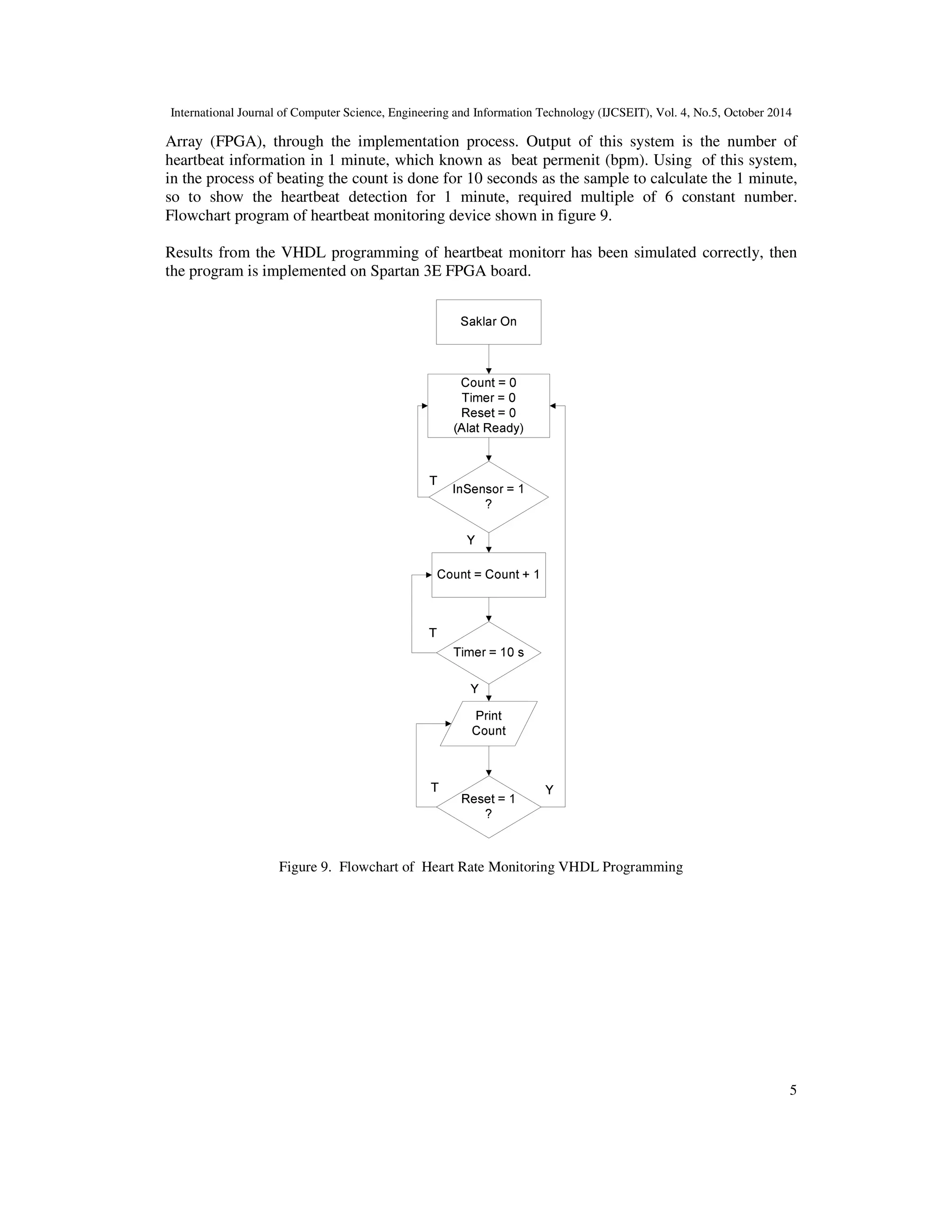
This document describes the design and implementation of an FPGA-based heart rate monitoring device using an optical fingertip sensor. The device consists of several blocks: an optical sensor unit to detect blood flow, a signal conditioning unit to filter and amplify the sensor signal, a pulse counter unit implemented on the FPGA to count heartbeats, a 10-second timer unit, and a display unit. Testing on 10 respondents found the device had an average error rate of 3.94% compared to a commercial oxymeter. The results demonstrate the feasibility of using an FPGA-based design with an optical sensor for basic heart rate monitoring.
![International Journal of Computer Science, Engineering and Information Technology (IJCSEIT), Vol. 4, No.5, October 2014
FPGA BASED HEARTBEATS MONITOR WITH
FINGERTIP OPTICAL SENSOR
Wahyu Kusuma R.1, Ridha I.2, Yasman Rianto3, Swelandiah E.P4
1,3 Departement of Electrcal Engineering, Gunadarma University, Jakarta, Indonesia
2,4 Departement of Computer Science, Gunadarma University, , Jakarta, Indonesia
ABSTRACT
The heart is an organ of human body which has a vital function, small abnormalities can have a big impact
on the performance of the body. Heart disease is the number one cause of death in the world. Examination
of the heart can be detected from blood flow in the fingertips, in order to obtain information about the
number and rhythm of the heartbeat. This research aims to design and implement the FPGA board to
monitor the heart rate with optical sensors.The results of this study are expected to facilitate the patient's
medical team or independently in detecting heart health. The series is composed of blocks of sensors,
signal conditioning block, the block pulse counter, block timer 10 seconds and blocks the viewer. Based on
the test results of the 10 respondents with a variety of age and gender, has built a tool that the percentage
error of 3.94%.
KEYWORDS
Heartbeat monitor, Xilinx ISE Webpack, FPGA, optical sensor
1. INTRODUCTION
The heart is an organ of human body which has a vital function, small abnormalities can have a
big impact on the performance of the heart kita.Penyakit body is the number one cause of death
in the world. Based on data from the World Health Organization (WHO), cardiovascular disease
has reached 29% in the percentage of deaths in the world and 17 million people die every year
due to heart and blood vessel disease throughout the world [3].
The development of medical instrumentation systems is growing rapidly along with the need for
medical personnel to diagnose a patient and a medical examination. One medical instrumentation
used for the examination of the heart is Electrocardiograph (ECG). ECG is a medical instrument
that is commonly used by the medical team to detect heart rate and rhythm [6]. EKG can not be
used independently by patients to detect a patient's pulse. In addition to the expensive costs for
the procurement of ECG, ECG devices also require special skills to operate.
Along with the requirement in the design and manufacture of medical devices, digital electronics
design technology is developing very rapidly, both in terms of hardware and software. Xilinx is
one manufacturer that produces equipment or tools for modeling the design of digital systems.
One product is in the form of a kit module board FPGA (Field Programmable Gate Array).
FPGA is a programmable device that is composed of large modules independent logic that can be
configured by the user who is connecting through the canals of programmable routing [4].
DOI : 10.5121/ijcseit.2014.4501 1](https://image.slidesharecdn.com/fpgabasedheartbeatsmonitorwith-141111214238-conversion-gate01/75/Fpga-based-heartbeats-monitor-with-1-2048.jpg)
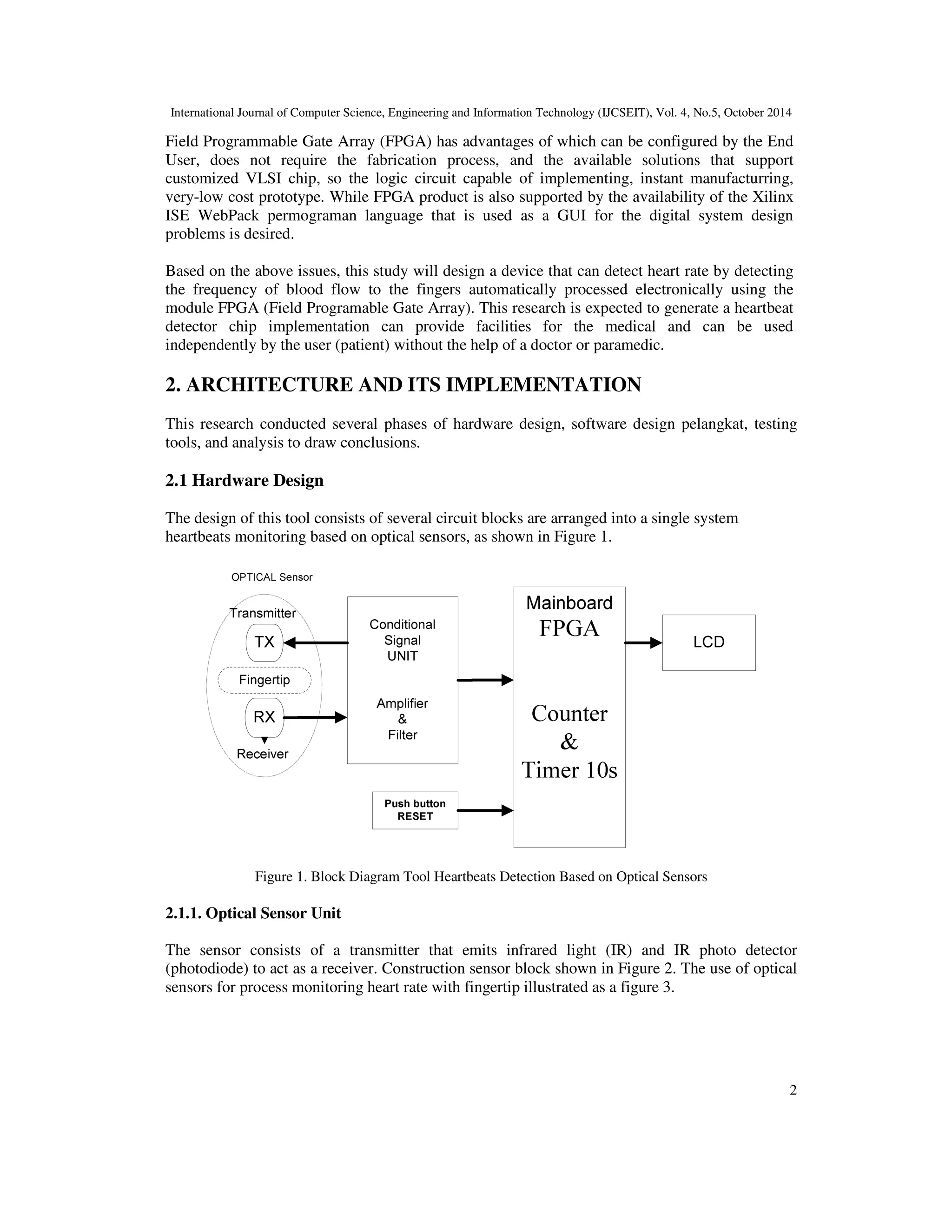
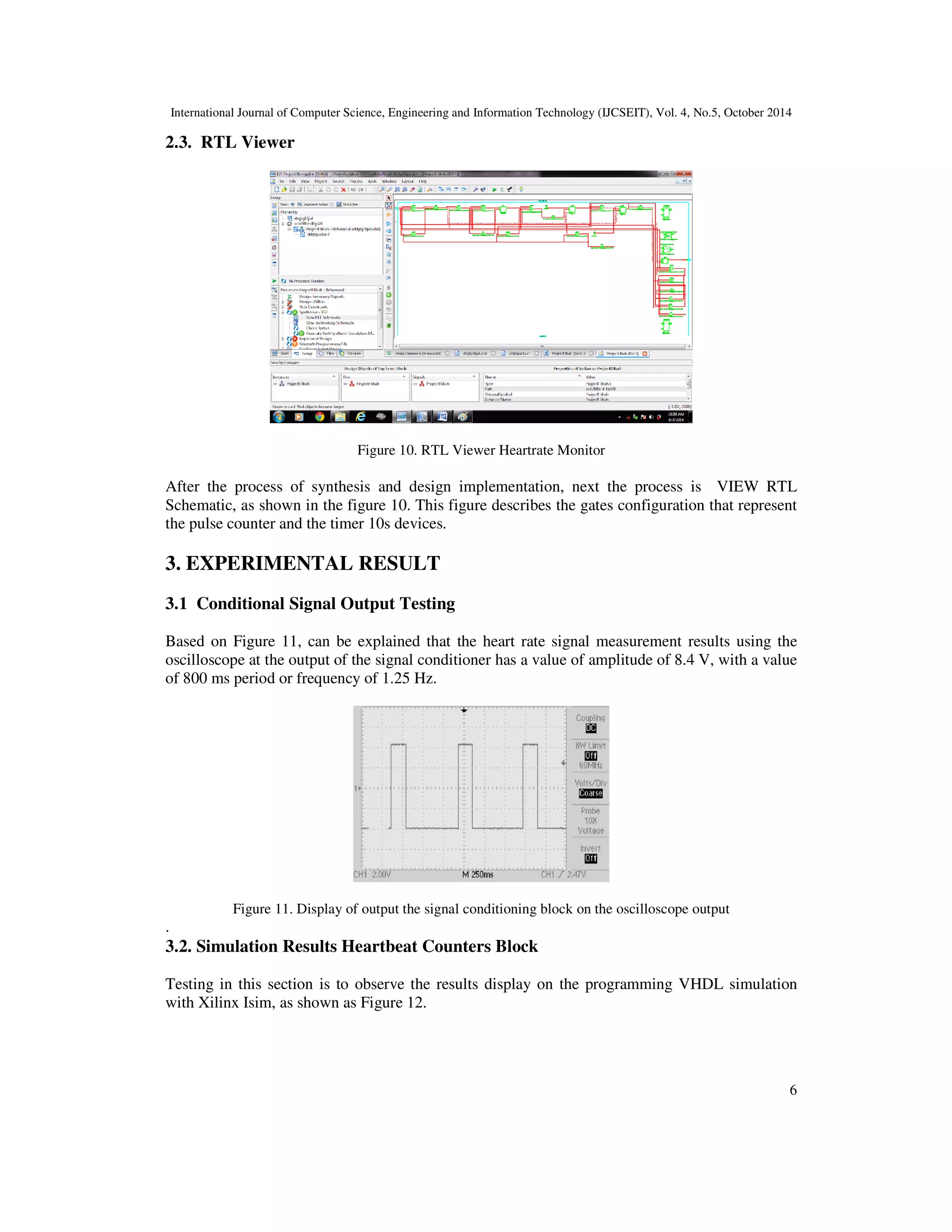
![International Journal of Computer Science, Engineering and Information Technology (IJCSEIT), Vol. 4, No.5, October 2014
counter block is designed with programming languages Xlinx WebPack ISE. The design of the
pulse counter block is shown as figure 6.
4
Figurer 6. Design of Heart Counter Unit
2.1.4. Timer 10s Unit
This block is designed for pulse counting process is done by calculating the input signal to the
timer block rate for 10 seconds. The basic principle of the timer unit is a clock signal frequency
divider circuit. The clock signal is taken from the internal oscillator signal frequency of 50 MHz
on the FPGA module. In order to get a signal with a period of 20 seconds, then beat signal as a
function of the timer must have a frequency of 50 mHz, by taking half the period of the high
level. The output signal timer 10s unit to be input to the Enable signal (En) at the pulse counter
block. The timer 10s unit is shown in Figure 7.
Figure 7. Diagram Block of Timer 10s
2.1.5. Display Unit
The Display unit that is used is the 6 Led (D5, D4, D3, D2, D1, D0) which represents the value of
the output of the pulse counter block. In addition, the results of the calculation rate is also
displayed with an LCD unit. This block already exists in the module of Spartan 3E FPGA Starter
Kit [4], as shown in the figure 8.
Figure 8. Display of LED and LCD at FPGA Spartan 3E Starter Kit [4]
2.2. Designing of Programming Xilinx ISE Webpack
In this research, design of Xilinx ISE Webpack program done on the pulse counter block and
block the timer 10s. The programming result, then applied to the module Field Programable Gate](https://image.slidesharecdn.com/fpgabasedheartbeatsmonitorwith-141111214238-conversion-gate01/75/Fpga-based-heartbeats-monitor-with-4-2048.jpg)
![International Journal of Computer Science, Engineering and Information Technology (IJCSEIT), Vol. 4, No.5, October 2014
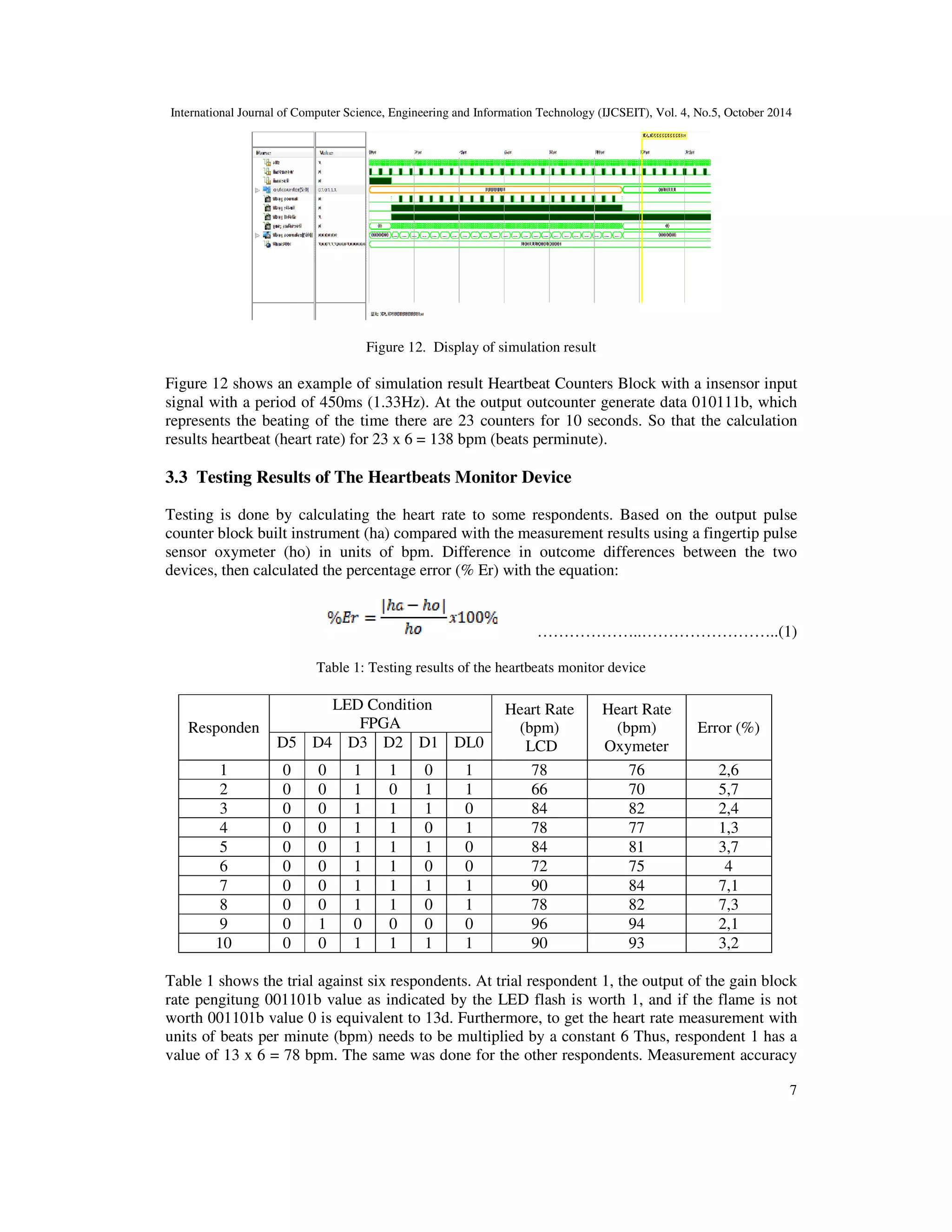
in terms of percentage error is calculated using equation (1). Based on the test results in Table 1,
it has been tested tool designed to measure the number of heartbeats to 10 respondents, has an
error (Error) an average of 3.94%.
8
4. CONCLUSION
This research has successfully designed a heartbeat monitor circuit using the Xilinx ISE program
WebPack 13.1. The series is composed of sensors block, signal conditioning block, pulse counter
block, timer 10s unit and the display unit. Based on the test results of the 15 respondents, a tool
designed to have a percentage error of 3.28%.
5. SUGESTION
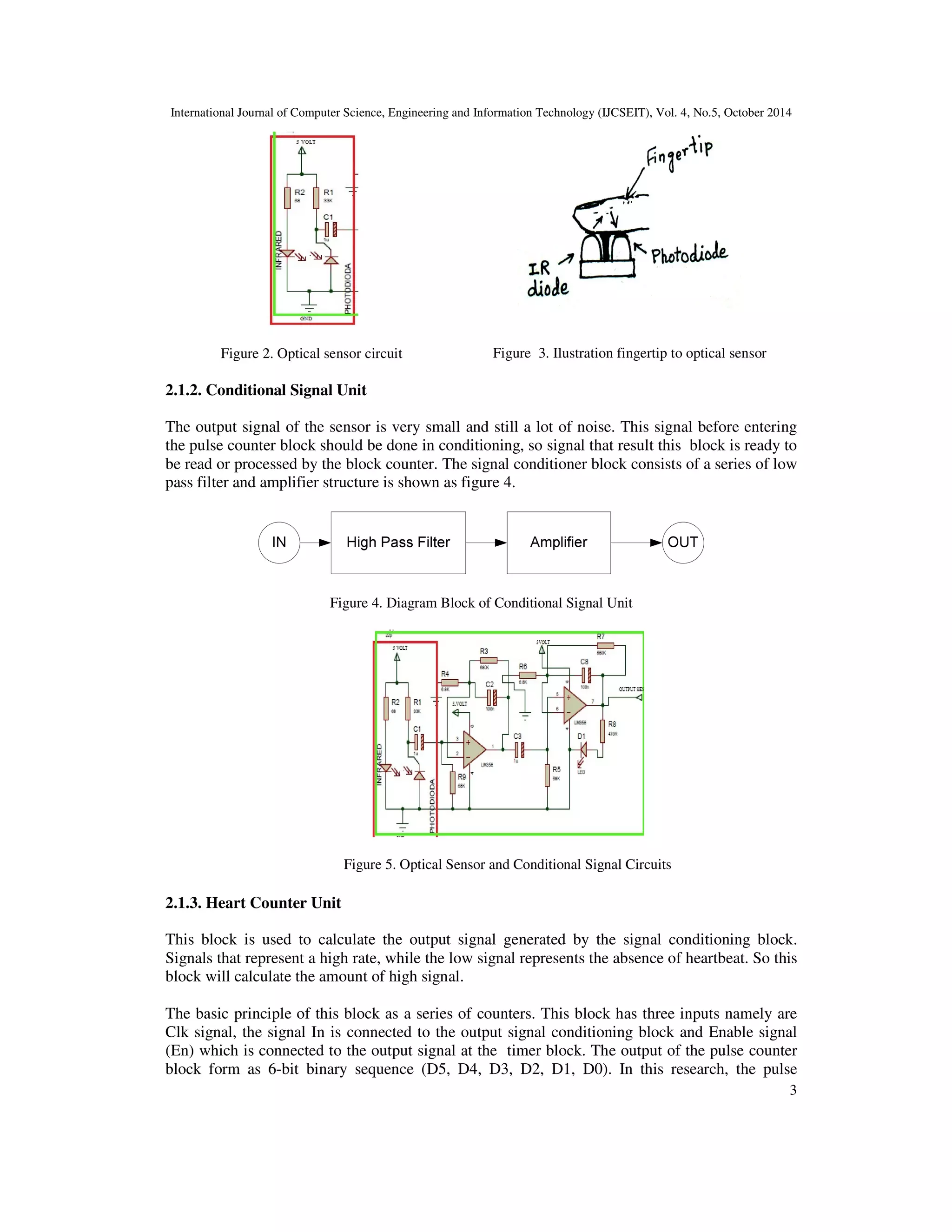
a. In the testing process, the accuracy of the optical sensor is strongly influenced on laying /
finger placement ujuag. So to overcome this required the manufacture of containers or the
media, so the detection of blood flow in the fingertips can be precision quickly.
b. In the signal conditioning block in this research, design and manufacturing are still using
electronic components. In further studies need to be developed to block the signal conditioner
made with vhdl programming, thus forming sauté specific integrated circuits or ASICs known
(Application-Specific Integrated Circuits)
Figure 13. FPGA based heartbeats monitor circuit
Optical Sensor
Conditional Signal
Circuit
REFERENCES
[1] Dogan., I., Kadri., B, 2012, Hear Rate Measurement from the Finger using a low cost
Microcontroller, http://www.emo.org.tr/ekler/ a568a2aa8c19a31_ek. pdf,
[2] Machriz, E., Sony S., Achmad R., 2008, Perancangan Perangkat Monitoring Denyut Jantung (Heart-
Beat Monitoring) dengan Visualisasi LCD Grafik Berbasis ATMEL AT89C51, proseding
Konferensi Nasional Sistem dan Informatika 2008; Bali, November 15, 2008.
[3] Hadiyani N., , 2012, Penyakit Jantung Koroner, http://www.dokterku-online.
com/index.php/article/54-penyakit-jantung-koroner, 14 Februari 2014
[4] Pong P. C., 2008, FPGA Prototyping by VHDL Examples: Xilinx Spartan-3 Version, Publisher:
Wiley-Interscience
[5] Sharief F. B., Liena E., Abdel K., Samah M. E., 2011, Microcontroller Based Heart Rate Monitor
using Fingertip Sensors, UofKEJ Vol. 1 Issue 2 pp. 47-51,October 2011
[6] Webster, EDS, 1981, Design of Microcomputer-Base Medical Instrumentation, Prentice Hall
International, New Jersey
Xilinx Spartan 3E
FPGA](https://image.slidesharecdn.com/fpgabasedheartbeatsmonitorwith-141111214238-conversion-gate01/75/Fpga-based-heartbeats-monitor-with-8-2048.jpg)