This is about the comparison between BJTs and FETs and about their types. Drain and Transfor characteristics of both. Different types of amplifiers.Circuit diagrams are given with details description.
This is about the comparison between BJTs and FETs and about their types. Drain and Transfor characteristics of both. Different types of amplifiers.Circuit diagrams are given with details description.
I have made this ppt in a way such that it will be able for viewers to understand easily and also have included construction and advantages of EMT and also I have compared it with Piezoelectric Transducers for better gain and videos for testing of EMT.
Analytical Modeling of Tunneling Field Effect Transistor (TFET)Abu Obayda
Tunneling Field-Effect Transistor (TFET) has emerged as an alternative for conventional CMOS by enabling the supply voltage, VDD, scaling in ultra-low power, energy efficient computing, due to its sub-60 mV/decade sub-threshold slope (SS). Given its unique device characteristics such as the asymmetrical source/drain design induced unidirectional conduction, enhanced on-state Miller capacitance effect and steep switching at low voltages, TFET based circuit design requires strong interactions between the device-level and the circuit-level to explore the performance benefits, with certain modifications of the conventional CMOS circuits to achieve the functionality and optimal energy efficiency. Because TFET operates at low supply voltage range (VDD<0.5V) to outperform CMOS, reliability issues can have profound impact on the circuit design from the practical application perspective. In this thesis report, we have analyzed the drain current characteristics of TFET with respect channel length. From our simulation result, it is observed that the drain current is minimum with respect to increasing channel length for Si and the drain current decreases for all the materials when the channel length is increased and after normalization lowest value of drain current is got for 10nm channel length.
In this paper, we present current amplifier based transimpedance amplifier (TIA) for biosensor applications. Proposed design has low-noise, high Transimpedance gain that can be used for low current measurement applications. The current amplifier based TIA is implemented in order to resolve the fabrication issues related to high value feedback resistor. In this design, the input block to TIA is a low amplitude current amplifier. The designed amplifier is implemented in 90 nm complementary metal-oxide semiconductor (CMOS) technology. The design achieves transimpedance gain of 800 kΩ with a bandwidth of 5 kHz and input referred current noise is of 0.152 pA/√𝐻𝑍 for an input of 41 nA bypassed from current amplifier with input of 200 pA.
The three terminals of the FET are known as Gate, Drain, and Source.
It is a voltage controlled device, where the input voltage controls by the output current.
In FET current used to flow between the drain and the source terminal. And this current can be controlled by applying the voltage between the gate and the source terminal.
So this applied voltage generate the electric field within the device and by controlling these electric field we can control the flow of current through the device.
Building a Raspberry Pi Robot with Dot NET 8, Blazor and SignalR - Slides Onl...Peter Gallagher
In this session delivered at Leeds IoT, I talk about how you can control a 3D printed Robot Arm with a Raspberry Pi, .NET 8, Blazor and SignalR.
I also show how you can use a Unity app on an Meta Quest 3 to control the arm VR too.
You can find the GitHub repo and workshop instructions here;
https://bit.ly/dotnetrobotgithub
MATHEMATICS BRIDGE COURSE (TEN DAYS PLANNER) (FOR CLASS XI STUDENTS GOING TO ...PinkySharma900491
Class khatm kaam kaam karne kk kabhi uske kk innings evening karni nnod ennu Tak add djdhejs a Nissan s isme sniff kaam GCC bagg GB g ghan HD smart karmathtaa Niven ken many bhej kaam karne Nissan kaam kaam Karo kaam lal mam cell pal xoxo
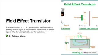
1. Field Effect Transistor
A field-effect transistor, or FET, is a type of transistor used for amplifying or
switching electronic signals. In this presentation, we will explore the different
types of FETs, their working principles, and their applications.
by Satyasis Mishra
2. MOSFET
Power MOSFETs
Used in power electronics, from electric vehicles to
power supplies.
CMOS transistors
Used in digital circuits, from processors to memory
chips.
Metal-Oxide-Semiconductor Field-Effect Transistors, or MOSFETs, come in many varieties for different
applications. They can be found in power electronics, such as electric vehicles and power supplies, as well as
in digital circuits, such as processors and memory chips.
3. JFET
Amplification
Used for signal amplification in audio and radio frequency (RF) circuits.
Sensitivity
Sensitive to voltage so can be used for touch switches and digital potentiometers.
Low-Noise performance
Used in low-noise high-impedance preamplifiers applications.
Junction Field-Effect Transistors, or JFETs, are used for signal amplification in audio and radio
frequency circuits because of their high input impedance. Due to their sensitivity to voltage, they are
also used for touch switches and digital potentiometers. Low-noise, high-impedance preamplifiers is
another application of JFETs.
4. MESFET
1 Analog Amplifiers
Used for microwave and millimeter-wave amplification.
2 Integrated Circuits
Used in integrated circuits, such as those made from gallium arsenide.
3 RF Switches
Used in microwave/millimeter-wave switches, such as those used in wireless devices.
Metal Semiconductor Field-Effect Transistors, or MESFETs, are used for microwave and millimeter-wave
amplification. They are also used in integrated circuits, such as those made from gallium arsenide, and in
microwave/millimeter-wave switches for wireless devices.
5. Principle
N-Channel FET
On applying a positive voltage to the gate, an
electric field is produced that reduces the resistance
of the channel.
P-Channel FET
On applying a negative voltage to the gate, an
electric field is produced that increases the
resistance of the channel.
The principle of the FET is based on controlling the flow of current through a semiconductor channel using an
electric field. When a voltage is applied to the gate, an electric field is produced that either reduces or
increases the resistance of the semiconductor channel, depending on the type of FET.
6. Applications
1 Amplifiers
FETs are used for signal
amplification in audio and
radio frequency circuits.
2 Switches
FETs are used as
switches in power
electronics and in
microwave/millimeter-
wave switches for
wireless devices.
3 Sensors
Due to their sensitivity to
voltage, FETs are used
as sensors for touch
switches and digital
potentiometers.
Field-effect transistors (FETs) have a wide range of applications, including signal amplification, power
electronics, microwave/millimeter-wave switches, and as sensors for touch switches and digital
potentiometers.
7. Advantages & Disadvantages
Advantages
• High input impedance - low loading effect
• High-frequency response
• Low noise
• No biasing needed
Disadvantages
• Sensitivity to temperature changes
• Less rugged than BJTs
• No beta - more susceptible to
variations in manufacturing
Field-Effect Transistors (FETs) have several advantages over bipolar junction transistors (BJTs), including
high input impedance, high-frequency response, low noise, and no biasing needed. However, FETs are
sensitive to temperature changes, less rugged than BJTs, and more susceptible to variations in
manufacturing.
8. Comparison with BJTs
Property Bipolar Junction Transistor
(BJT)
Field-Effect Transistor (FET)
Principle of operation Current controlled Voltage controlled
Input impedance Low High
Gain (beta) High No beta
Noise High Low
Switching speed Low to moderate High
FETs and Bipolar Junction Transistors (BJTs) have different principles of operation, with BJTs being current
controlled and FETs being voltage controlled. FETs have a higher input impedance, lower noise, and faster
switching speed than BJTs. However, BJTs have a high gain (beta) while FETs do not.
9. Future Prospects
1 Improving FET Performance
Research is focused on reducing power consumption, improving noise performance,
increasing the frequency range, and extending the lifetime of FETs.
2 New Applications
FETs are being explored for applications in quantum computing, terahertz-frequency
electronics, and energy efficiency in power electronics.
3 New FET Technologies
New materials, such as 2D materials and organic semiconductors, are being explored for
use in FETs.
The future of FET technology is bright, with research focused on improving performance, exploring new
applications, and developing new FET technologies using materials such as 2D materials and organic
semiconductors. FETs are being explored for use in quantum computing, terahertz-frequency electronics,
and for improving energy efficiency in power electronics.