This document provides instructions for a practical evaluation in a computer aided design course. Students are tasked with using AutoCAD to produce technical drawings, including an electrical wiring layout for a home. The procedures outline how to set up layers for different elements, import design files, and print the completed drawings with various layer combinations. The goal is for students to practice precision drawing of schematics and wiring diagrams using AutoCAD commands. A reflection section at the end allows students to comment on what they learned from the exercise.
ECE321322 Electronics I & Lab Spring 2015 1 Final P.docxjack60216
ECE321/322 Electronics I & Lab Spring 2015
1
Final Project – Demo. Review Form
Student name:
Item Comments Grade
Simulation verification
Are the transformer and overall
power supply working
/10
Are the pre/main
amplifiers work?
/10
Final breadboard setup and test
Power supply works?
/10
Is Preamp design approach
correct and the board working?
/10
Is main amplifier design correct
and working?
/10
Lab skills
Proficient with lab equipment
and testing?
/10
Overall grade /60
ECE321/322 Electronics I & Lab Spring 2015
1
Final Project – Report Review Form
Student name:
Item Comments Grade
Project report
Report format as specified?
/10
Technical discussion with
simulation and measurement
data?
(Ability to analyze and design
complex electrical and electronic
devices)
/10
Did theory cover sufficient
details to compare and justify
experimental data?
(Knowledge and ability to apply
mathematics)
/10
Appendix: Pspice source files
and other info (e.g., data
sheet)?
/10
Overall grade /40
1
ECE 321 Final Project
This project is for individual student and is NOT a team project.
HOWEVER, collaboration among team members (i.e., ECE322 team) is strongly
encouraged and should be properly acknowledged in the final project report.
Final Project Report Due: May 4, 2015 to be uploaded onto Evaltools
Project Demo:
Tues., 5/5/15, 1:30 - 3:30 For TTH Classes that meet at 3:00 pm (ECE 322_01)
Wed., 5/6/15, 1:30 - 3:30 For MWF Classes that meet at 3:00 pm (ECE 322_02)
Objective
1. To design an “analog computer” to fulfill the following requirement
Vout = 25*(A*V1in + B*V2in)
where V1in = V2in = 10 mVpp @ 1 kHz, is the input sinusoidal (sine) signal to the analog
computer, which can be generated from a function generator; Vout is the output of the
computer; and A is a constant of your birth month mod 10 (divide by 10 and take the
remainder) and B is a constant of your birth day mod 10 (divide by 10 and take the
remainder).
e.g., If your birthday is November 7, A = 11 mod 10 = 1 and B = 7 mod 10 = 7.
If your birthday is February 26, A = 2 mod 10 = 2 and B = 26 mod 10 = 6.
2. To verify the circuit design with the help of contemporary software
3. To build and test the final design on breadboard
Instructions and Related Information
Figure 1 shows an illustrative block diagram of the analog computer.
Figure 1. Block diagram of an “analog computer”
2
DC dual-polarity power supply:
1. It should be able to provide a stable ±12V dc power.
2. 7812 and 7912 voltage regulators are available (datasheets are available at
AllUser U:\ECE Component Library on lab workstations). If you are using your
own laptop, you need to type \\ECEVault\AllUser\ECE Component Library.
3. Refer to the figure below (read Chapter 17 of your textbook):
...
EELE 5331 Digital ASIC DesignLab ManualDr. Yushi Zhou.docxtoltonkendal
EELE 5331: Digital ASIC Design
Lab Manual
Dr. Yushi Zhou
Department of Electrical Engineering
Lakehead University
Thunder Bay, Ontario, Canada
Contents
1 Introduction . . . . . . . . . . . . . . . . . . . . . . . . . . . . 2
2 MOSFET Devices and Layout Tutorial . . . . . . . . . . . . . 4
2.1 Prepare For Schematic . . . . . . . . . . . . . . . . . . 4
2.2 Perform Simulation . . . . . . . . . . . . . . . . . . . . 7
2.3 Layout . . . . . . . . . . . . . . . . . . . . . . . . . . . 11
2.4 Layout Veri�cation . . . . . . . . . . . . . . . . . . . . 17
2.5 Report . . . . . . . . . . . . . . . . . . . . . . . . . . . 25
2.6 How to understand DRC error report . . . . . . . . . . 26
3 CMOS Inverter . . . . . . . . . . . . . . . . . . . . . . . . . . 27
3.1 Design speci�cations . . . . . . . . . . . . . . . . . . . 27
3.2 Lab Procedure . . . . . . . . . . . . . . . . . . . . . . 29
3.3 Report . . . . . . . . . . . . . . . . . . . . . . . . . . . 31
1
EELE5331:Digital ASIC Design [email protected]
1 Introduction
This lab manual is an essential components of EELE5331: Digital ASIC
Design, o�ered by Dr. Yushi Zhou. The lab works consists of schematic
entry, symbol generation, pre-layout simulation, layout, physical and logic
veri�cation, extraction and post-layout simulation for the design. All the
students are required to submit individual lab report before the deadline.
All reports must be typed and professionally prepared. The content that
needs to be included in the report are given at the end of each lab. There
are total three labs, and each part will be released before the lab starts.
• Lab 1: MOSFET devices and layout tutorial
• Lab 2: CMOS Inverter
• Lab 3: CMOS Digital Logic Circuits
It should be noted that the students are not limited to the assigned lab
time, which may not be enough to complete the lab. Students are expected
to work on the lab during their free time if that case is required. You may
use remote log-in to complete the labs.
TSMC CMOS 180 nm technology process design kit (PDK) is a 1-Poly,
6-Metal technology, with a maximum supply voltage of 1.8 V for thin oxide
devices and 3.3 V for thick oxide devices. This process is suitable for design-
ing analog, digital, RF and mixed-signal circuits and systems. In this course,
all the labs are designed based upon CMOS 180 nm process. The computer-
aided design (CAD) tools that are adopted in this course are from Cadence
Design Systems for the purpose of schematic entry, simulation, implemen-
tation and veri�cation. The Cadence custom IC design platform provides
a graphical interface for various stages in the design �ow. An overview of
the design �ow and which tools are involved in each stage is shown in Fig.1.
As you may notice that there are loops, indicating iterative procedures. For
instance, if the physical layout does not pass design rules check or LVS check,
Page 2
EELE5331:Digital ASIC Design [email protected]
the modi�cation of.
108EN Electrical and Electronic scienceDesign, Simulation .docxpaynetawnya
108EN Electrical and Electronic science
Design, Simulation and Technical Report
Place a picture of your hardware design
Contents
List of Figures 0
List of Tables 0
Part A: DC circuits [15 marks] 1
Introduction (5 Marks) 1
Design and simulation (35 Marks) 1
Hardware design (10 Marks) 2
Part C Results (10 Marks) 3
Part C (10 Marks) 4
Conclusions and Recommendations (5 Marks) 5
References (5 Marks) 5
Appendix (optional) 5
1
List of Figures
Figure 1: The simulated circuit1
Figure 2: The designed decoder2
Figure 3: The hardware circuit2
Figure 4: Priority encoder3List of Tables
Table 1: Truth table2
Part A: Semiconductor Devices, LO 5,6 [10 marks]
Take a photo of your constructed circuit [1 mark]
Insert a screenshot showing the signal across the load resister[4marks]
Explain the produced graph and steps you followed to accomplish it. This should prove your ownership of the design and understanding of the functions of MyDaq kit [5 marks].
Part B: Digital Circuits LO 3,6 [75 marks]Introduction (5 Marks)
Briefly summarise your project and steps followed to accomplish it. This should be written last and should be short (about 100 to 150 words). It should emphasize briefly the basis or reasons for the experiment. In addition, the methodology/ procedure, analysis, significant findings, conclusions and recommendations are also expected to be summarised concisely (in few sentences bearing in mind the number of words limitation).
The introduction should include an introductory paragraph that details the relevance of this lab to the demonstration of engineering principles.
A few paragraphs should be written that give good examples of where this work occurs in industry/ engineering design etc (Provide some figures of relevant application).
Introduce very briefly the rest of the Lab report sections here.
Hardware design (15 Marks)
Provide a brief description of all elements used in building the circuits (Push buttons, Pull-up resistors, Inverters, decoders, 7-segment resistors and 7-segment), suggestions and further improvements. Use the datasheets provided via Moodle or any other references. Use Harvard referencing guide found on Moodle.
Figure 3: The hardware circuit
Figure 4: Priority encoder
Figure 5: Common Anode 7 segment display (Source: ElectronicsTutorials)
Use Harvard referencing. Design and simulation (35 Marks)
Figure 1: The simulated circuit on Multisim
Re-design the SN7447A IC using logic gates, explain how and what you have done. Provide background theory and math (Boolean) where appropriate.
Table 1: Truth table
Clearly labelled photographs or schematics (often preferable) of the equipment are required.
Figure 2: The designed decoder on Multisim
It is important to show evidence of deep gained knowledge.
Conclusions and Recommendations (5 Marks)
This section (100 – 200 words) should briefly summarise the main conclusions of the laboratory exercise. What comes first, simulation or hardware c ...
This document provides standards for all electrical schematic diagrams for the LHC and its detectors. It covers:
- High and low voltage distribution diagrams.
- Relay and automatism diagrams.
- Lighting, power and earth protection diagrams.
- LHC main ring magnets cabling diagrams.
- Cooling and ventilation relay and automatism diagrams.
AutoCAD is a basically a drafting software used by engineers and architects for 2-D ,3-D drafting of houses,schematics,mechanical ,electrical devices and it is a substitute for pen & paper used for decades. Designs can created quickly using the AutoCAD and it is also widely used standalone software for designing. AutoCAD is also very helpful for clothing, Jewellary, landscape designer basically whosoever needs things to be drawn electronically, easily and quickly use AutoCAD
Layout Design of Low Power Half Adder using 90nm Technology IJEEE
The basic building block of any digital operation is addition. This paper compares fully automatic and proposed semicustom layout design; the proposed design has been optimized for power consumption, low area and high speed. Power consumption and area are the major design issue for a designer. All the design result of fully custom and proposed semicustom design taken at 1.2V. In this the circuit simulation has been done on DSCH3 and layout simulation on Microwind3.1.
How to Create Map Views in the Odoo 17 ERPCeline George
The map views are useful for providing a geographical representation of data. They allow users to visualize and analyze the data in a more intuitive manner.
How to Split Bills in the Odoo 17 POS ModuleCeline George
Bills have a main role in point of sale procedure. It will help to track sales, handling payments and giving receipts to customers. Bill splitting also has an important role in POS. For example, If some friends come together for dinner and if they want to divide the bill then it is possible by POS bill splitting. This slide will show how to split bills in odoo 17 POS.
Welcome to TechSoup New Member Orientation and Q&A (May 2024).pdfTechSoup
In this webinar you will learn how your organization can access TechSoup's wide variety of product discount and donation programs. From hardware to software, we'll give you a tour of the tools available to help your nonprofit with productivity, collaboration, financial management, donor tracking, security, and more.
Model Attribute Check Company Auto PropertyCeline George
In Odoo, the multi-company feature allows you to manage multiple companies within a single Odoo database instance. Each company can have its own configurations while still sharing common resources such as products, customers, and suppliers.
Unit 8 - Information and Communication Technology (Paper I).pdfThiyagu K
This slides describes the basic concepts of ICT, basics of Email, Emerging Technology and Digital Initiatives in Education. This presentations aligns with the UGC Paper I syllabus.
2024.06.01 Introducing a competency framework for languag learning materials ...Sandy Millin
http://sandymillin.wordpress.com/iateflwebinar2024
Published classroom materials form the basis of syllabuses, drive teacher professional development, and have a potentially huge influence on learners, teachers and education systems. All teachers also create their own materials, whether a few sentences on a blackboard, a highly-structured fully-realised online course, or anything in between. Despite this, the knowledge and skills needed to create effective language learning materials are rarely part of teacher training, and are mostly learnt by trial and error.
Knowledge and skills frameworks, generally called competency frameworks, for ELT teachers, trainers and managers have existed for a few years now. However, until I created one for my MA dissertation, there wasn’t one drawing together what we need to know and do to be able to effectively produce language learning materials.
This webinar will introduce you to my framework, highlighting the key competencies I identified from my research. It will also show how anybody involved in language teaching (any language, not just English!), teacher training, managing schools or developing language learning materials can benefit from using the framework.
2024.06.01 Introducing a competency framework for languag learning materials ...
End of chapter problem 6
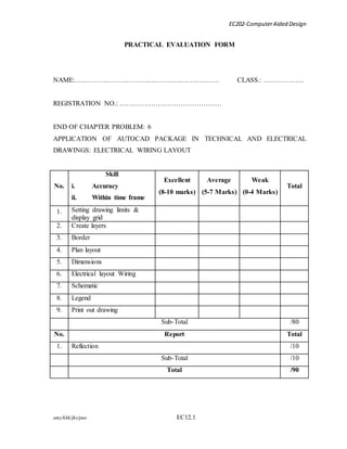
1. EC202-Computer Aided Design
PRACTICAL EVALUATION FORM
NAME:………………………………………………………. CLASS.: ………………
REGISTRATION NO.: ………………………………………
END OF CHAPTER PROBLEM: 6
APPLICATION OF AUTOCAD PACKAGE IN TECHNICAL AND ELECTRICAL
DRAWINGS: ELECTRICAL WIRING LAYOUT
No.
Skill
i. Accuracy
ii. Within time frame
Excellent
(8-10 marks)
amy/khk/jke/puo EC12.1
Average
(5-7 Marks)
Weak
(0-4 Marks)
Total
1. Setting drawing limits &
display grid
2. Create layers
3. Border
4. Plan layout
5. Dimensions
6. Electrical layout Wiring
7. Schematic
8. Legend
9. Print out drawing
Sub-Total /80
No. Report Total
1. Reflection /10
Sub-Total /10
Total /90
2. EC202-Computer Aided Design
END OF CHAPTER PROBLEM: 6
TITLE : APPLICATION OF AUTOCAD PACKAGE IN TECHNICAL AND
ELECTRICAL DRAWINGS
COURSE LEARNING OUTCOME:
CLO 5: Produce with precision the drawings of graphics, electronic circuits
schematics and electrical wiring layout diagrams faster and neat.
OBJECTIVES: The students should be able to:
1. Draw accurately and neatly electrical wiring layout plan for home, office
or at any specified space.
2. Make use of the AutoCAD commands such as the Draw, Edit, Drawing
Aid commands skillfully to produce technical drawings.
EQUIPMENT : 1. Desktop Computer/Laptop
2. AutoCAD 2004 software
3. Printer for A3/A4 (Black/Color)
PROCEDURE:
1. Create a new drawing space using the Metric measurement.
2. Set the drawing limits to A4 paper size.
3. Display the grid to the extent of the drawing limits.
4. Create layers and rename the layers as below:
i. Border
ii. Plan Layout
iii. Dimension
iv. Electrical Wiring Layout
v. Schematic
vi. Legend
amy/khk/jke/puo EC12.2
3. EC202-Computer Aided Design
5. Make layer Border as the current layer and redraw to full scale size Fig 12.1
6. Refer to Fig. 12.2.
Make the layer Plan Layout as the current layer and draw the Plan Layout of
the home and name each area/space/room.
Make layer dimension as the current layer and place dimensions to the plan
layout.
Make the layer Electrical Wiring as the current layer and draw the electrical
components and the wiring layout.
Make the layer Schematic as the current layer and draw the schematic circuit
as in Fig. 12.3.
Make the Layer Legend as the current layer and redraw the diagram /symbols
as in Table 12.1.
7. Print out the drawing file as follows:
i. Layers Border and Plan Layout.
ii. Layers Border, Plan Layout and Dimension.
iii. Layers Border, Plan Layout and Electrical Wiring.
iv. Layers Border, Schematic and Legend.
8. Save the drawing file and exit AutoCAD.
amy/khk/jke/puo EC12.3
5. EC202-Computer Aided Design
Fig. 12.2: Layout plan of Domestic House for a Single-Single Phase
Electrical Installation
Fig. 12.3: Schematic diagram of a Single-phase Electrical Installation
amy/khk/jke/puo EC12.5
6. EC202-Computer Aided Design
Table 12.1: Legend for the Electrical Wiring & Schematic Diagram
REFLECTION:
At the end of this practical work, I have learnt that:
…………………………………………………………………………………………………
…………………………………………………………………………………………………
…………………………………………………………………………………………………
amy/khk/jke/puo EC12.6
(10 Marks)