This edition contains two articles providing new insights in a relevant field for future nano-electronics applications, i.e. molecular computing at the atomic scale. Since 1974, Molecular electronics had been always associated to the possible future of computers. A new European
Integrated Project AtMol was proposed and accepted by the European Commission after the FP7 ICT Call 6 to create this new technology (www.atmol.eu). The nanoICT “Mono-Molecular Electronics” Working Group was also set-up in 2008 to reach this objective.
In 2010, the nanoICT project launched its first call for exchange visits for PhD students with the following main objectives: 1. To perform joint work or to be trained in the leading European industrial and academic research institutions; 2. To enhance long-term collaborations within
the ERA; 3. To generate high-skilled personnel and to facilitate technology transfer;
The first outcome report (“Heat dissipation in nanometer-scale ridges”) of this call investigates experimentally the effect of lateral confinement of acoustic phonons in silicon ridges as a function of the temperature.
We would like to thank all the authors who contributed to this issue as well as the European Commission for the financial support (projects nanoICT No. 216165 and AtMol No. 270028).
Vital Alert Communication, a pioneer in the utilization of Very Low Frequency (VLF) technology for use in communications & positioning in GPS denied environments, announce the release of "MAGI-SIM". MAGI-SIM is an innovative simulation tool for VLF propagation modeling.
OPTIC NANO Consult S.A.R.L provides scientific support in spectroscopic ellipsometry and polarimetry metrology for thin films and new materials. It was founded in 2011 and collaborates with research institutes, laboratories, and foundries. OPTIC NANO aims to give expert attention and advice within global research projects, using complementary advanced measurement techniques and modeling to investigate new products and materials while preserving confidentiality. The company's expertise comes from years of research experience in optics and relationships with instrument developers.
OptiFDTD is a finite-difference time-domain (FDTD) simulation software that enables the design and simulation of photonic components. It solves Maxwell's equations to model light propagation and interactions with materials. OptiFDTD provides a comprehensive set of materials, excitation sources, and analysis tools. New features include 64-bit support for larger simulations, heating absorption modeling, plane wave phase control, and band solvers. It is suited for applications like photonic crystals, nonlinear optics, integrated photonics, and more.
The document provides highlights of new features in COMSOL Multiphysics 4.3. Key additions include nonlinear material models, 1D pipe flow and network simulations, electrochemical corrosion simulations, faster CAD import and meshing, AC/DC electromagnetics for rotating machinery, improved nonlinear solvers, and new modules for thermoacoustics and piezoresistivity. The product suite now supports additional CAD formats and LiveLink products provide tighter integration with CAD software.
1) The document presents a novel design for a grating coupled optical waveguide surface plasmon excitation mechanism as an alternative to the traditional prism coupling approach used in surface plasmon resonance sensors.
2) Computational modeling and simulation of the design was carried out using COMSOL Multiphysics software to analyze the electromagnetic field distribution.
3) The results of the modeling confirm the viability of the design and warrant further research into signal decoupling characteristics and response to refractive index changes in the analyte layer.
Pengolahan air-limbah-domestik-dengan-metode-biology-irigation-memanfaatkan-e...Andien Ingin Sukses
Gagasan ini menawarkan metode biology irigation untuk mengolah limbah domestik dengan memanfaatkan tanaman eceng gondok. Eceng gondok dapat menyerap limbah organik dan anorganik sehingga dapat meningkatkan kualitas air limbah. Metode ini dilakukan dengan menciptakan saluran irigasi dimana air limbah akan mengalir melalui bak-bak penampungan yang berisi eceng gondok untuk menyerap limbah sebelum masuk ke perairan. Diharapkan dap
El documento presenta cuatro restaurantes de Benissa, España: Bon Gust, Casa Cantó, Casa del Maco y Tapas Vizcaíno. Cada restaurante ofrece una breve descripción de su historia, menús de degustación que incluyen platos típicos locales y bebidas, y sus horarios. El documento promueve la gastronomía tradicional de Benissa.
El documento habla sobre las ventajas de tener una página web y participar en redes sociales versus solo tener una página estática. Sugieren construir una presencia digital 2.0 a través de un blog, redes como LinkedIn, y herramientas colaborativas para darse a conocer y generar nuevos negocios. También ofrecen un servicio de consultoría para diagnosticar, diseñar, construir, capacitar sobre y dar seguimiento a una instalación digital que funcione como un abrevadero de información para la actividad de una empresa.
SKOS Thesaurus Editing which makes use of "Linked Data". A lot of facts from the Semantic Web (e.g. from DBpedia) can be used to augment local thesauri or knowledge bases. This video shows how PoolParty Thesaurus Management makes use of data from the Semantic Web.
Este documento describe el servicio SMS Cloud de IPBusiness. Ofrece envíos masivos y personalizados de mensajes de texto a través de una interfaz web sin necesidad de infraestructura por parte del cliente. Incluye características como capacidad de envío customizable, compatibilidad multiplataforma y facilidad de uso. Describe dos tipos de envíos: unilateral para informar y bilateral para informar y recibir respuestas para gestión personalizada. Resalta los beneficios como priorización de envíos, capacidad adaptable, reportes en tiempo real y calidad de serv
Influence of time and length size feature selections for human activity seque...ISA Interchange
In this paper, Viterbi algorithm based on a hidden Markov model is applied to recognize activity sequences from observed sensors events. Alternative features selections of time feature values of sensors events and activity length size feature values are tested, respectively, and then the results of activity sequences recognition performances of Viterbi algorithm are evaluated. The results show that the selection of larger time feature values of sensor events and/or smaller activity length size feature values will generate relatively better results on the activity sequences recognition performances.
Este documento describe los servicios disponibles en la Universidad Técnica de Machala, incluyendo la biblioteca virtual, biblioteca digital, aula virtual, servicios médicos y ontologicos, Google Apps institucionales, repositorio académico, sistema de inscripción y bienestar estudiantil. Explica brevemente la función de cada servicio y diferencia una biblioteca virtual de una biblioteca digital.
Een Joomla-webshop bouwen zonder webshop-extensie, met formulierenAnja de Crom
Stel, je hebt een website waarop je maar een paar dingen wilt verkopen. Workshops bijvoorbeeld, of je eigen boek, of aandelen voor een crowdfundingsactie of… Dan kun je daarvoor een webshopextensie installeren. Maar dat is voor die vijf workshops of dat ene boek misschien toch wat veel van het goede. Het kan anders: met formulieren.
Met behulp van de extensies RSForm!Pro en cciDEAL kun je zonder webshop toch producten en diensten verkopen via je website. Mét of zonder iDEAL, met directe betaling of betaling achteraf, na ontvangst van de factuur.
Goed om te weten: de manier waarop je voor deze webshop-zonder-webshop met formulieren omgaat kun je ook gebruiken voor andere toepassingen.
This document discusses the fabrication and characterization of ultrathin tungsten molybdenum oxide films for electrochromic applications. Nanoparticle inks were synthesized using a hydrothermal method and spray coated onto substrates. Spray coating produced thinner films than drop casting, with nanoparticles assembling during drying. Heating the substrate during spraying helped eliminate oxygen vacancies. The spray coated films exhibited higher transmittance in the bleached state and higher contrast in the colored state compared to drop cast films, with contrast density over 10 times greater. Kinetics testing showed faster coloration and bleaching times for the spray coated films.
Ponte en Forma es una tienda online que vende suplementos vitamínicos y ofrece asesoría personalizada para mejorar la condición física. Su misión es complementar una alimentación saludable con suplementos de calidad para apoyar el desarrollo deportivo. Su visión es convertirse en la mejor tienda online para la venta de suplementos deportivos en Colombia para 2017 con más de 20 mil clientes.
NRB Group groeide de voorbije vijf jaar uit tot een belangrijke ICT-dienstverlener in België, met een geconsolideerde omzet van 222 miljoen euro (+ 7% tegenover 2013). Een resem overnames speelde daarin een belangrijke rol. CEO Ulrich Penzkofer licht toe welke rol hij daar ziet voor zijn finance en voor zijn hr-team.
La televisión IP permite ver contenido audiovisual a través de Internet de forma interactiva y a la carta. Hulu ofrece series, películas y deportes en streaming con publicidad o mediante suscripción. Sus ingresos crecen rápidamente pero Google planea competir con YouTube. La televisión del futuro podría ser una batalla entre estas plataformas que ofrezcan la mejor experiencia al usuario.
Las obras de teatro tienen las siguientes características: 1) Los autores deben contar una historia, 2) Se debe lograr un clímax entre los autores y el público, 3) Es un espectáculo completo donde la acción es determinada por el autor.
La empresa COMEC,C.A. se dedica a la comercialización y fundición de metales como el aluminio, fundada en 1990 en Ciudad Guayana. Actualmente comercializa aluminio lingoteado de 600 kg obtenido mediante fusión en hornos de más de 5 toneladas. Para llevar a cabo sus procesos de fundición y recuperación de escoria utiliza equipos como cintas transportadoras, gandolas y payloader.
Haciendo el contenido comprensible para estudiantes de InglésAntonio Piedra
El documento describe los componentes claves del modelo SIOP (Sheltered Instruction Observation Protocol) para enseñar efectivamente lenguaje y contenido. Estos incluyen definir claros objetivos de contenido y lenguaje, usar materiales para hacer las lecciones significativas, y proporcionar actividades auténticas que integren conceptos con práctica del idioma. También enfatiza vincular nuevos conceptos con experiencia previa, usar variedad de técnicas para hacer conceptos claros, y proporcionar oportunidades para que los estudiantes usen estrategias y
Este documento presenta un manual de apoyo para docentes que imparten la asignatura estatal "Formación Ciudadana Democrática para la construcción de una Cultura de la Legalidad" en México. Se explica el origen y propósito de la asignatura, así como los estados donde se imparte actualmente. El manual provee información sobre los contenidos temáticos, aprendizajes esperados, ejemplos de lecciones y actividades, y recursos adicionales para apoyar a los docentes en la enseñanza de esta asignatura.
Presented by Nick Yoo, Senior Director of Information Security Architecture and Services, McKesson at ForgeRock Open Identity Stack Summit, June 2013
Learn more about ForgeRock Access Management:
https://www.forgerock.com/platform/access-management/
Learn more about ForgeRock Identity Management:
https://www.forgerock.com/platform/identity-management/
2014 Membership Marketing Benchmarking Presentation by Tony RossellTony Rossell
It is my pleasure to announce the release of the 2014 Membership Marketing Benchmarking Report.
This marks the sixth year that Marketing General Incorporated (MGI) has surveyed associations to better understand what is going on in the membership market and what is working best to recruit members, engage new members, renew existing members, and reinstate former members. It also marks the highest level of association participation with 865 separate associations sharing their data.
The 2014 Report includes new questions related to social media usage, email frequency and open rates, and who pays membership dues (individuals or companies).
A free download of the full report is available from the Marketing General Incorporated website.
Nanotechnology Presentation For Electronic Industrytabirsir
Nanoelectronics aims to process, transmit, and store information using properties of matter at the nanoscale that are different from macroscale properties. Relevant length scales are a few nanometers for molecules acting as transistors or memory, and up to 999 nm for quantum dots using electron spin. While microelectronics uses gate sizes as small as 50 nm, it does not qualify as nanoelectronics as it does not exploit new physical properties related to reduced size.
This document discusses applications of nanotechnology including nanocells, carbon nanotubes, and molecular electronics. Nanocells are self-assembled networks of metallic particles that act as programmable switches. Carbon nanotubes are rolled sheets of carbon that can be semiconductors or metals and are strong candidates for nanowires. Potential applications highlighted include using carbon nanotubes for transistors, fuel cells, and simulation. Other applications discussed are nanobridge devices, nanoscale transistors, components for quantum computers, nanophotonic devices, and nanobiochips for drug discovery.
The document discusses teaching nanoelectronics and provides examples. It summarizes the Institute for Nanoelectronics at TUM, which conducts research in areas like nanoimprinting, organic device fabrication and characterization, and multiscale modeling. It also outlines the evolution of nanoelectronics from More Moore to Beyond Moore approaches, providing examples of nanoscale devices and their potential applications. The challenges of teaching nanoelectronics are discussed, along with the programs available at TUM.
The Dielectric Relaxation Properties And Dipole Ordering...Sarah Gordon
The document describes the fabrication of a flexible field effect transistor (FET) using low-cost and biodegradable materials. Cellulose paper is used as both the substrate and dielectric layer, while pencil graphite is used as the source, drain, channel and gate without any other materials. Electron and hole mobilities of 180 and 200 cm2v-1s-1 respectively are observed for the all-carbon FET. The FET shows potential for motion detection applications through strain sensing.
IEEE Student Branch Chittagong University arranged a webinar titled "From APECE to ASML A Semiconductor Journey". Shawn Millat shared his working experience in Semiconductor industry and also shared tips about studying in Germany.
During the last decades a large effort has been invested in the development of a new
discipline devoted to benefit from optical excitations in materials where metals are
key element (Plasmonics). We will make an introduction on this topic below, but let’s
anticipate that two application areas are sensing and information technologies.
The following height extended abstracts, presented during the one-day NANOMAGMA
Symposium (Bilbao, Spain – April 13, 2011 reflects some of the latest developments on magneto-plasmonics.
In 2010 and 2011, the nanoICT project (EU/ICT/FET Coordination Action) launched
two calls for exchange visits for PhD students with the following main objectives: 1.
To perform joint work or to be trained in the leading European industrial and academic research institutions; 2. To enhance long-term collaborations within the ERA; 3. To
generate high-skilled personnel and to facilitate technology transfer;
The first outcome report was published in the issue 22 (August 2011) and this edition
contains four new articles providing insights in relevant fi elds for nanoICT.
We would like to thank all the authors who contributed to this issue as well as the European Commission for the financial support (projects nanoICT No. 216165 and NANOMAGMA No. FP7-214107-2).
Dr. Antonio Correia Editor - Phantoms Foundation
Nano electrical and electronic devices: advantages - Data storage
and memory - Micro and nanoelectromechanical systems - Lasers,
lighting and displays – Batteries - Fuel cells - Photovoltaic cells -
Electric double layer capacitors - Nanoparticle coatings for
electrical products
Performance evaluation of reversible logic based cntfet demultiplexer 2IAEME Publication
This document discusses the design and analysis of a reversible logic based carbon nanotube field effect transistor (CNTFET) demultiplexer. It presents the realization of 1:2 and 1:4 demultiplexers using reversible logic gates implemented with CNTFETs. Simulation results show the transient response and power consumption of the reversible logic CNTFET demultiplexers, with 0.8 and 1.6 nanowatts for the 1:2 and 1:4 designs respectively. This is compared to conventional CMOS demultiplexer designs, showing an improvement in power reduction achieved with the reversible logic CNTFET approach. Challenges in CNT fabrication that could impact robust circuits are also discussed.
Performance evaluation of reversible logic based cntfet demultiplexer 2IAEME Publication
This document discusses the design and analysis of a reversible logic based carbon nanotube field effect transistor (CNTFET) demultiplexer. It presents the realization of 1:2 and 1:4 demultiplexers using reversible logic gates implemented with CNTFETs. Simulation results show the transient response and power consumption of the reversible logic CNTFET demultiplexers, with 0.8 and 1.6 nanowatts for the 1:2 and 1:4 designs respectively. This is compared to conventional CMOS demultiplexer designs, showing an improvement in power reduction achieved with the reversible logic CNTFET approach. Challenges in fabricating robust CNT-based circuits are also discussed.
Mobile Systems
Instructor: Mark Bohr, Intel Corp.
• Technology trend and key challenges.
• Underlying system/application requirements.
• Interaction between circuit design and technology: transistor, interconnects, memory.
Integrated Power Electronics
Instructor: Tomas Palacios, MIT
• Technology trend and key challenges.
• Underlying system/application requirements.
• Interaction between circuit design and technology: transistor, interconnects, passive.
Memory Technologies
Instructor: Mark Johnson, Micron Technology
• Technology trend and key challenges.
• Underlying system/application requirements.
• Interaction between circuit design and technology: transistor, interconnects, passive.
Design for
The document discusses CMOS VLSI design technology and future trends. It provides an overview of CMOS technology and basic MOSFET operation. It then discusses how nanotechnology and integrated tri-gate transistors can help address limitations of CMOS scaling by reducing feature sizes and parasitic leakage. The document concludes that continued CMOS scaling will eventually be limited and alternatives like nanotechnology may be needed to retain device characteristics at smaller sizes.
Designing High-Speed, Low-Power Full Adder Cells Based on Carbon Nanotube Tec...VLSICS Design
This article presents novel high speed and low power full adder cells based on carbon nanotube field effect
transistor (CNFET). Four full adder cells are proposed in this article. First one (named CN9P4G) and
second one (CN9P8GBUFF) utilizes 13 and 17 CNFETs respectively. Third design that we named
CN10PFS uses only 10 transistors and is full swing. Finally, CN8P10G uses 18 transistors and divided into
two modules, causing Sum and Cout signals are produced in a parallel manner. All inputs have been used
straight, without inverting. These designs also used the special feature of CNFET that is controlling the
threshold voltage by adjusting the diameters of CNFETs to achieve the best performance and right voltage
levels. All simulation performed using Synopsys HSPICE software and the proposed designs are compared
to other classical and modern CMOS and CNFET-based full adder cells in terms of delay, power
consumption and power delay product.
322253456-NANOELECTRONICS-ppt of engineeringt24042567
This document discusses nanoelectronics and single electron transistors. It begins with definitions of nanotechnology and nanoelectronics, which generally refers to semiconductor devices at the nanoscale. It then describes single electron transistors, which use controlled electron tunneling to amplify current or measure single electron movement. SETs have two tunnel junctions that create a Coulomb island, and electrons can only enter by tunneling through the junctions. SETs have potential applications as supersensitive electrometers, in temperature and current standards, and for voltage/charge state logic. However, challenges remain around lithography techniques, background charge, co-tunneling, and operating at room temperature before SETs can be incorporated into practical devices.
This document discusses nanocomputing and quantum computing. It covers architectures like quantum dot cellular automata and crossbar switching. It discusses how nanocomputers would work using quantum states and spins. Applications of quantum computing include breaking codes and optimization problems. Challenges include maintaining the fragile quantum states long enough to perform computations. Overall, nanoscale quantum computing could revolutionize computing by massively increasing computing power.
This document discusses nanoelectronics and single electron transistors. It begins by defining nanotechnology as the manipulation of materials at the nanoscale, below 100 nm. Nanoelectronics refers to shrinking semiconductor devices to the nanoscale. A single electron transistor is described as a switching device that uses controlled electron tunneling and can measure single electron movement. It consists of a coulomb island between two tunnel junctions. For an electron to enter the island, its energy must exceed the coulomb energy barrier. Single electron transistors have potential applications as ultrasensitive electrometers and for voltage and charge state logic due to their small size and low power consumption. However, challenges remain regarding lithography, background charges, and operating them at room temperature
This document provides an overview of nanoelectronics. It defines nanoelectronics as a branch of engineering that uses electronic components with dimensions measured in nanometers. The document discusses how nanoelectronics can be used to reduce the size of electronic devices. It also outlines several applications of nanoelectronics in electronics, energy, and displays. Finally, it discusses future opportunities for nanoelectronics in areas like flexible electronics, wireless devices, and molecular devices.
We have calculated the minimum chip area overhead and hence the bit density reduction. In this approach,
the number of faults in each line of a memory block (matrix) is counted, and the lines having the largest
number of defects are replaced with the spare lines. This method achieved by memory array reconfiguration
(bad bit exclusion), combined with error correction code techniques, in prospective terabit-scale hybrid
semiconductor/nanodevice memories, as a function of the nanodevice fabrication yield and the micro-to-nano
pitch ratio. The results show that by using the best (but hardly practicable) reconfiguration and block size
optimization, hybrid memories with a pitch ratio of 10 may overcome purely semiconductor memories in
useful bit density if the fraction of bad nanodevices is below ∼15%, while in order to get an
order-of-magnitude advantage in density, the number of bad devices has to be decreased to ∼2%. For the
simple ‘Repair Most’ technique of bad bit exclusion, complemented with the Hamming-code error correction,
these numbers are close to 2% and 0.1%, respectively. When applied to purely semiconductor memories, the
same technique allows us to reduce the chip area ‘swelling’ to just 40% at as many as 0.1% of bad devices.
We have also estimated the power and speed of the hybrid memories and have found that, at a reasonable
choice of nanodevice resistance, both the additional power and speed loss due to the nanodevice subsystem
may be negligible.
DESIGNING HIGH-SPEED, LOW-POWER FULL ADDER CELLS BASED ON CARBON NANOTUBE TEC...VLSICS Design
This article presents novel high speed and low power full adder cells based on carbon nanotube field effect transistor (CNFET). Four full adder cells are proposed in this article. First one named CN9P4G) and second one (CN9P8GBUFF) utilizes 13 and 17 CNFETs respectively. Third design that we named CN10PFS uses only 10 transistors and is full swing. Finally, CN8P10G uses 18 transistors and divided into two modules, causing Sum and Cout signals are produced in a parallel manner. All inputs have been used straight, without inverting. These designs also used the special feature of CNFET that is controlling the threshold voltage by adjusting the diameters of CNFETs to achieve the best performance and right voltage levels. All simulation performed using Synopsys HSPICE software and the proposed designs are compared to other classical and modern CMOS and CNFET-based full adder cells in terms of delay, power consumption and power delay product.
Design of magnetic dipole based 3D integration nano-circuits for future elect...VIT-AP University
Nano Magnetic Logic (NML) has been attracting application in optical computing, nanodevice formation, and low power. In this paper nanoscale architecture such as the decoder, multiplexer, and comparator are implemented on perpendicular-nano magnetic logic (pNML) technology. All these architectures with the superiority of minimum complexity and minimum delay are pointed. The proposed architectures have been designed using pNML in MagCAD tool, simulated with modelsim platform and correctness shown by simulation waveform. The correctness of these designs can be verified easily when Verilog code is generated from MagCAD tool. The performance of the proposed comparator towards default parameters shows the area of 2.4336 μm2 and critical path of 1.5E-7 sec. As a higher order, the realization of a 4-to-1 multiplexer in NML has also been included in this work.
EVALUATION OF RADIATED EMISSIONS FROM PCB AND CABLES AT POST-LAYOUT LEVELPiero Belforte
This document presents a study evaluating methods to predict radiated emissions from printed circuit boards (PCBs) and attached cables at the design stage. It tests models of the radiated emissions of simple two-layer PCBs with and without an attached cable by comparing simulations to measurements. For PCBs alone, a model using Hertzian dipoles accurately predicts differential mode emissions. A more accurate model is then presented which considers both differential and common mode emissions, where common mode radiation is caused by ground noise on the PCB. The document finds that accounting for this ground noise is important when a cable is attached to the PCB, as the cable can be excited by this common mode signal. Improving the models to predict emissions earlier
This catalogue: (version 7.0, updated January 2017), compiled by the Phantoms Foundation (coordinator of the Spanish Nanotechnology Plan funded by ICEX), provides a general overview of the Nano Companies (104) in Spain and in particular the importance of this market research, etc.
This version includes also tech transfer institutions in Spain from universities, technological institutes, etc
This document aims at presenting Nanophononics to attract all the relevant stakeholders and help them to synergize into a vast but sound and well defined field. This call is made in direction of academic members, industries, SMEs and governmental organizations to join the European nanophononics community (www.euphonon.eu)
This document provides a catalogue of 106 nano companies in Spain as well as other tech transfer institutions, compiled by the Phantoms Foundation. It includes general information about each company such as main research areas, number of employees in R&D, percentage dedicated to nanotechnology, funded projects, patents, and contacts. The Phantoms Foundation focuses on structuring and fostering nanoscience and nanotechnology in Europe and collaborates with Spanish and European government institutions on related reports and initiatives.
On behalf of the Organising and the International Scientific Committees we take great pleasure in welcoming you to Genoa for the sixth edition of the Graphene and 2D Materials International Conference & Exhibition.
Over the past 5 editions, the Graphene Conference strengthened its position as the main meeting point of the Graphene community Worldwide.
Graphene2016 will feature:
A plenary session with internationally renowned speakers
An industrial forum focused on Graphene Commercialization
Extensive thematic workshops in parallel
(Metrology, Characterization & Standardization, Health & Medical Applications, Theory & Simulation, Production & Applications of graphene and related materials, Energy and Worldwide Graphene Initiatives, Funding & Priorities)
An important exhibition carried out with the latest Graphene trends
A Brokerage event
Graphene2016 is now an established event, attracting global participants intent on sharing, exchanging and exploring new avenues of graphene-related scientific and commercial developments.
Phantoms Foundation is pleased to launch the third edition of the Graphene companies catalogue. This new version features also the research centers currently performing work on graphene worldwide. In total 136 institutions (Companies: 119 & Research Centers: 17) working directly on the field are presented.
This initiative comes as an open platform resource to attract global participant’s intent on sharing, exchanging and exploring new avenues of graphene-related scientific and commercial developments.
This document announces the 1st International Workshop on Graphene Industry - Challenges & Opportunities taking place in Zaragoza, Spain. The workshop aims to present the current state of graphene materials/devices and industrial opportunities, focusing on recent technology advances and business opportunities in graphene commercialization. It seeks to develop relationships that accelerate graphene's industrial growth. The event brings together representatives from graphene companies and labs to share market visions and business opportunities in current applications. It will provide an overview of graphene developments and innovations in the functional materials industry.
Now on its 4th edition, nanoPT will be organized in Braga at the INL (The International Iberian Nanotechnology Laboratory). The conference will be held with the purpose of strengthen ties nationally and internationally on Nanotechnology and will encourage industry and universities working on the Nanotechnology field to know each other and to present their research.
nanoPT2016 structure will keep the fundamental features of the previous editions, providing a unique opportunity for broad interaction. However, following the success of the past 3 editions nanoPT2016 is now a 4 days conference instead of the usual 3 days.
The conference will cover a broad range of topics on current research in Nanoscience and Nanotechnology from high level speakers and also an exhibition. nanoPT 2016 is an excellent platform to exchange ideas, networking, find new partners and understand the current state of the art in nanotechnology.
This E-nano Newsletter issue contains the Strategic Research Agenda for Nanophononics, one of the main outputs of the EUPHONON coordination action (www.euphonon.eu); EU project with the mission to build a European Community for Nanophononics. The main objective of the Nanophononics Strategic Research Agenda is to define the role and impact of nanophononics in today’s society and in the industry. It is expected to give insight to the potential of the field to improve the properties of current information technology devices, enhance energy efficiency and advance the health and well-being and safety. In addition research highlights from top-level research institutions worldwide such as MANA/NIMS (Japan) and CIC nanoGUNE (Spain) are presented.
Graphene Position Paper (E-Nano Newsletter Special Issue)Phantoms Foundation
This E-nano Newsletter special issue contains the final version of the nanoICT position paper on Graphene (one-atom-thick sheet of carbon / in 2010, A.K. Geim
and K. Novoselov, were awarded the Nobel Prize in physics for “groundbreaking experiments regarding the two-dimensional material graphene”) summarising the
current state of progress and open perspectives concerning the emergence of graphene-based technologies and applications. This paper is a mixture between a short review of recent achievements and ingredients for the elaboration of a more specific and detailed roadmap.
This second version of the report “Nanoscience & Nanotechnology in Spain” provides insights by identifying R&D directions and priorities in Spain. Moreover, it aims to be a valid source of guidance, not only for the scientific community but also for the industry.
This report covers a wide range of interdisciplinary areas of research and development, such as Graphene, Nanochemistry, Nanomedicine, Carbon
Nanotubes, Nanomaterials for Energy, Modelling, etc., and provides insights in these areas, currently very active worldwide and particularly in Spain. It
also provides an outlook of the entire Spanish nanotechnology system, including nearly 250 research institutions and over 50 companies.
Expected impact of initiative s suc h a s this document is to enhance visibility, ommunication and networking between specialists in several
fields, facilitate rapid information flow, look for
areas of common ground between different technologies and therefore shape and consolidate the Spanish and European research communities.
This catalogue : (2 nd version, updated November 3, 2011),
compiled by the Phantoms Foundation (coordinator of
the Spanish Nanotechnology action plan funded by
ICEX), provides a general overview of the Nanoscience
and Nanotechnology companies (78) in Spain and in particular the importance of this market research,
product development, etc.
Note: only those contacted companies which provided
their details are listed.
Graphene for Emerging Technologies - Workshop booklet (October 2011)Phantoms Foundation
Workshop “Graphene for Future Emerging Technologies: Challenges and Opportunities”.
This workshop presented the current state of the art and the opportunities of
graphene-based materials/devices and related structures for future emerging
technologies in the field of Information and Communication Technologies (ICT). Focus
was made on identifying the directions of promising innovation and disruptive
technologies, including flexible electronics and transparent conductors, high frequency
devices, digital logic, spintronics, nanoelectromechanical devices, ultimate sensors and
bio-related applications. Challenges in the fields of ultimate microelectronics, energy dissipation and thermal management, advanced composites for aeronautics, and large
scale graphene production and device integration were discussed.
At this stage, it is impossible to predict the exact course
the nanotechnology revolution will take and, therefore,
its effect on our daily lives. We can, however, be
reasonably sure that nanotechnology will have a
profound impact on the future development of many
commercial sectors. The impact will likely be greatest in
the strategic nanoelectronics (ICT nanoscale devices -
nanoICT) sector, currently one of the key enabling
technologies for sustainable and competitive growth in
Europe, where the demand for technologies permitting
faster processing of data at lower costs will remain
undiminished.
Considering the fast and continuous evolvements in the
inter-disciplinary field of Nanotechnology and in
particular of “ICT nanoscale devices”, initiatives such as
the nanoICT Coordination Action 1 should identify and
monitor the new emerging fields research drivers of
interest for this Community and put in place
instruments/measures to address them.
One of the main challenges is the timely identification
and substantiation of new directions for the physical
realisation of ICT beyond CMOS that have a high
potential for significant breakthrough and that may
become the foundations of the information and
communication technologies and innovations of
tomorrow.
Therefore, the first version of the nanoICT research
agenda provides focus and accelerate progress in
identified R&D directions and priorities for the
“nanoscale ICT devices and systems” FET proactive
program and guide public research institutions, keeping
Europe at the forefront in research. In addition, it aims
to be a valid source of guidance, not only for the
nanoICT scientific community but also for the industry
(roadmapping issues), providing the latest developments in the field of emerging nano-devices that appear
promising for future take up by the industry.
This first version of the research agenda is an open
document to comments and/or suggestions and covers
a very wide range of interdisciplinary areas of research
and development, such as Mono-Molecular electronics,
Bioelectronics, NEMS, Nanotubes, Modelling, etc.
providing insights in these areas, currently very active
worldwide.
Expected impact of initiatives such as this nanoICT
strategic research agenda is to enhance visibility,
communication and networking between specialists in
several fields, facilitate rapid information flow, look for
areas of common ground between different
technologies and therefore shape and consolidate the
European research community.
I hope you will enjoy reading this document and look
forward to the next edition beginning of 2011 which will
explore some new nanoICT related research areas such
as Spintronics, Nanophotonics and Nanophononics.
Please contact coordinators of the working groups if
you are interested in providing a comment.
This E-nano Newsletter special double issue
contains the updated version of the nanoICT
position paper on Carbon Nanotubes (CNTs)
summarising state-of-the-art research in this field
as well as a description of the possible electrical,
electronic and photonic applications of carbon
nanotubes, the types of CNTs employed and the
organisations or groups that are most proficient
at fabricating them.
In the second paper, the Nanoelectronics
European Research Roadmap is addressed
focusing on the main European Programmes
supporting the short, medium and long-term
research activities.
This issue also contains a catalogue (insert),
compiled by the Phantoms Foundation
providing a general overview of the
Nanoscience and Nanotechnology
companies in Spain and in particular the
importance of this market research,
product development, etc.
We would like to thank all the authors
who contributed to this issue as well as
the European Commission for the
financial support (project nanoICT No.
216165).
Dr. Antonio Correia
Editor - Phantoms Foundation
www.phantomsnet.net
This document provides a catalogue of nanoscience and nanotechnology companies located in Spain. It includes overviews of several Spanish companies conducting research and development in areas such as nanocoatings, nanocomposites, drug delivery, nanomedicine, nanobio, nanochemistry, nanomaterials, nanoparticles, nanotubes, nanophotonics, modelling/simulation/software, and graphene. The catalogue was compiled by the Phantoms Foundation, a nonprofit organization focused on nanoscience and nanotechnology that coordinates Spain's national nanotechnology action plan funded by ICEX, the Spanish Institute for Foreign Trade.
Threats to mobile devices are more prevalent and increasing in scope and complexity. Users of mobile devices desire to take full advantage of the features
available on those devices, but many of the features provide convenience and capability but sacrifice security. This best practices guide outlines steps the users can take to better protect personal devices and information.
OpenID AuthZEN Interop Read Out - AuthorizationDavid Brossard
During Identiverse 2024 and EIC 2024, members of the OpenID AuthZEN WG got together and demoed their authorization endpoints conforming to the AuthZEN API
HCL Notes and Domino License Cost Reduction in the World of DLAUpanagenda
Webinar Recording: https://www.panagenda.com/webinars/hcl-notes-and-domino-license-cost-reduction-in-the-world-of-dlau/
The introduction of DLAU and the CCB & CCX licensing model caused quite a stir in the HCL community. As a Notes and Domino customer, you may have faced challenges with unexpected user counts and license costs. You probably have questions on how this new licensing approach works and how to benefit from it. Most importantly, you likely have budget constraints and want to save money where possible. Don’t worry, we can help with all of this!
We’ll show you how to fix common misconfigurations that cause higher-than-expected user counts, and how to identify accounts which you can deactivate to save money. There are also frequent patterns that can cause unnecessary cost, like using a person document instead of a mail-in for shared mailboxes. We’ll provide examples and solutions for those as well. And naturally we’ll explain the new licensing model.
Join HCL Ambassador Marc Thomas in this webinar with a special guest appearance from Franz Walder. It will give you the tools and know-how to stay on top of what is going on with Domino licensing. You will be able lower your cost through an optimized configuration and keep it low going forward.
These topics will be covered
- Reducing license cost by finding and fixing misconfigurations and superfluous accounts
- How do CCB and CCX licenses really work?
- Understanding the DLAU tool and how to best utilize it
- Tips for common problem areas, like team mailboxes, functional/test users, etc
- Practical examples and best practices to implement right away
Let's Integrate MuleSoft RPA, COMPOSER, APM with AWS IDP along with Slackshyamraj55
Discover the seamless integration of RPA (Robotic Process Automation), COMPOSER, and APM with AWS IDP enhanced with Slack notifications. Explore how these technologies converge to streamline workflows, optimize performance, and ensure secure access, all while leveraging the power of AWS IDP and real-time communication via Slack notifications.
Driving Business Innovation: Latest Generative AI Advancements & Success StorySafe Software
Are you ready to revolutionize how you handle data? Join us for a webinar where we’ll bring you up to speed with the latest advancements in Generative AI technology and discover how leveraging FME with tools from giants like Google Gemini, Amazon, and Microsoft OpenAI can supercharge your workflow efficiency.
During the hour, we’ll take you through:
Guest Speaker Segment with Hannah Barrington: Dive into the world of dynamic real estate marketing with Hannah, the Marketing Manager at Workspace Group. Hear firsthand how their team generates engaging descriptions for thousands of office units by integrating diverse data sources—from PDF floorplans to web pages—using FME transformers, like OpenAIVisionConnector and AnthropicVisionConnector. This use case will show you how GenAI can streamline content creation for marketing across the board.
Ollama Use Case: Learn how Scenario Specialist Dmitri Bagh has utilized Ollama within FME to input data, create custom models, and enhance security protocols. This segment will include demos to illustrate the full capabilities of FME in AI-driven processes.
Custom AI Models: Discover how to leverage FME to build personalized AI models using your data. Whether it’s populating a model with local data for added security or integrating public AI tools, find out how FME facilitates a versatile and secure approach to AI.
We’ll wrap up with a live Q&A session where you can engage with our experts on your specific use cases, and learn more about optimizing your data workflows with AI.
This webinar is ideal for professionals seeking to harness the power of AI within their data management systems while ensuring high levels of customization and security. Whether you're a novice or an expert, gain actionable insights and strategies to elevate your data processes. Join us to see how FME and AI can revolutionize how you work with data!
How to Get CNIC Information System with Paksim Ga.pptxdanishmna97
Pakdata Cf is a groundbreaking system designed to streamline and facilitate access to CNIC information. This innovative platform leverages advanced technology to provide users with efficient and secure access to their CNIC details.
Generating privacy-protected synthetic data using Secludy and MilvusZilliz
During this demo, the founders of Secludy will demonstrate how their system utilizes Milvus to store and manipulate embeddings for generating privacy-protected synthetic data. Their approach not only maintains the confidentiality of the original data but also enhances the utility and scalability of LLMs under privacy constraints. Attendees, including machine learning engineers, data scientists, and data managers, will witness first-hand how Secludy's integration with Milvus empowers organizations to harness the power of LLMs securely and efficiently.
HCL Notes und Domino Lizenzkostenreduzierung in der Welt von DLAUpanagenda
Webinar Recording: https://www.panagenda.com/webinars/hcl-notes-und-domino-lizenzkostenreduzierung-in-der-welt-von-dlau/
DLAU und die Lizenzen nach dem CCB- und CCX-Modell sind für viele in der HCL-Community seit letztem Jahr ein heißes Thema. Als Notes- oder Domino-Kunde haben Sie vielleicht mit unerwartet hohen Benutzerzahlen und Lizenzgebühren zu kämpfen. Sie fragen sich vielleicht, wie diese neue Art der Lizenzierung funktioniert und welchen Nutzen sie Ihnen bringt. Vor allem wollen Sie sicherlich Ihr Budget einhalten und Kosten sparen, wo immer möglich. Das verstehen wir und wir möchten Ihnen dabei helfen!
Wir erklären Ihnen, wie Sie häufige Konfigurationsprobleme lösen können, die dazu führen können, dass mehr Benutzer gezählt werden als nötig, und wie Sie überflüssige oder ungenutzte Konten identifizieren und entfernen können, um Geld zu sparen. Es gibt auch einige Ansätze, die zu unnötigen Ausgaben führen können, z. B. wenn ein Personendokument anstelle eines Mail-Ins für geteilte Mailboxen verwendet wird. Wir zeigen Ihnen solche Fälle und deren Lösungen. Und natürlich erklären wir Ihnen das neue Lizenzmodell.
Nehmen Sie an diesem Webinar teil, bei dem HCL-Ambassador Marc Thomas und Gastredner Franz Walder Ihnen diese neue Welt näherbringen. Es vermittelt Ihnen die Tools und das Know-how, um den Überblick zu bewahren. Sie werden in der Lage sein, Ihre Kosten durch eine optimierte Domino-Konfiguration zu reduzieren und auch in Zukunft gering zu halten.
Diese Themen werden behandelt
- Reduzierung der Lizenzkosten durch Auffinden und Beheben von Fehlkonfigurationen und überflüssigen Konten
- Wie funktionieren CCB- und CCX-Lizenzen wirklich?
- Verstehen des DLAU-Tools und wie man es am besten nutzt
- Tipps für häufige Problembereiche, wie z. B. Team-Postfächer, Funktions-/Testbenutzer usw.
- Praxisbeispiele und Best Practices zum sofortigen Umsetzen
Cosa hanno in comune un mattoncino Lego e la backdoor XZ?Speck&Tech
ABSTRACT: A prima vista, un mattoncino Lego e la backdoor XZ potrebbero avere in comune il fatto di essere entrambi blocchi di costruzione, o dipendenze di progetti creativi e software. La realtà è che un mattoncino Lego e il caso della backdoor XZ hanno molto di più di tutto ciò in comune.
Partecipate alla presentazione per immergervi in una storia di interoperabilità, standard e formati aperti, per poi discutere del ruolo importante che i contributori hanno in una comunità open source sostenibile.
BIO: Sostenitrice del software libero e dei formati standard e aperti. È stata un membro attivo dei progetti Fedora e openSUSE e ha co-fondato l'Associazione LibreItalia dove è stata coinvolta in diversi eventi, migrazioni e formazione relativi a LibreOffice. In precedenza ha lavorato a migrazioni e corsi di formazione su LibreOffice per diverse amministrazioni pubbliche e privati. Da gennaio 2020 lavora in SUSE come Software Release Engineer per Uyuni e SUSE Manager e quando non segue la sua passione per i computer e per Geeko coltiva la sua curiosità per l'astronomia (da cui deriva il suo nickname deneb_alpha).
Building Production Ready Search Pipelines with Spark and MilvusZilliz
Spark is the widely used ETL tool for processing, indexing and ingesting data to serving stack for search. Milvus is the production-ready open-source vector database. In this talk we will show how to use Spark to process unstructured data to extract vector representations, and push the vectors to Milvus vector database for search serving.
GraphRAG for Life Science to increase LLM accuracyTomaz Bratanic
GraphRAG for life science domain, where you retriever information from biomedical knowledge graphs using LLMs to increase the accuracy and performance of generated answers
Skybuffer SAM4U tool for SAP license adoptionTatiana Kojar
Manage and optimize your license adoption and consumption with SAM4U, an SAP free customer software asset management tool.
SAM4U, an SAP complimentary software asset management tool for customers, delivers a detailed and well-structured overview of license inventory and usage with a user-friendly interface. We offer a hosted, cost-effective, and performance-optimized SAM4U setup in the Skybuffer Cloud environment. You retain ownership of the system and data, while we manage the ABAP 7.58 infrastructure, ensuring fixed Total Cost of Ownership (TCO) and exceptional services through the SAP Fiori interface.
Presentation of the OECD Artificial Intelligence Review of Germany
Enano newsletter issue22
1. No. 22 /// August 2011 www.phantomsnet.net
Atomic Scale and Single Molecule
Logic Gate Technologies (AtMol)
Heat dissipation in nanometer-scale ridges
The raise up of UHV atomic scale
interconnection machines
2.
3. dear readers,
This edition contains two articles providing new insights in a relevant field for future nano-
electronics applications, i.e. molecular computing at the atomic scale. Since 1974, Molecular
electronics had been always associated to the possible future of computers. A new European
Integrated Project AtMol was proposed and accepted by the European Commission after
the FP7 ICT Call 6 to create this new technology (www.atmol.eu). The nanoICT “Mono-
Molecular Electronics” Working Group was also set-up in 2008 to reach this objective.
In 2010, the nanoICT project launched its first call for exchange visits for PhD students with
the following main objectives: 1. To perform joint work or to be trained in the leading European
industrial and academic research institutions; 2. To enhance long-term collaborations within
the ERA; 3. To generate high-skilled personnel and to facilitate technology transfer;
The first outcome report (“Heat dissipation in nanometer-scale ridges”) of this call
investigates experimentally the effect of lateral confinement of acoustic phonons in silicon
ridges as a function of the temperature.
We would like to thank all the authors who contributed to this issue as well as the European
Commission for the financial support (projects nanoICT No. 216165 and AtMol No. 270028).
> Dr. Antonio Correia Editor - Phantoms Foundation
contents
05 > nanoresearch. Atomic Scale and Single Molecule Logic Gate Technologies
(AtMol) /// C. Joachim
12 > nanoresearch. Heat dissipation in nanometer-scale ridges /// P.-O. Chapuis,
A. Shchepetov, M. Prunnila, S. Laakso, J. Ahopelto and C. M. Sotomayor Torres
18 > nanojobs
21 > nanoICT Conf Report
23 > nanoresearch. The raise up of UHV atomic scale interconnection machines /// J. S.
Prauzner-Bechcicki, D. Martrou, C. Troadec, S. Gauthier, M. Szymonski and C. Joachim
editorial information
No 22. August 2011. Published by Phantoms Foundation (Spain)
editor > Dr. Antonio Correia > antonio@phantomsnet.net
assistant editors > José Luis Roldán, Maite Fernández, Conchi Narros,
Carmen Chacón and Viviana Estêvão.
1500 copies of this issue have been printed. Full color newsletter
available at: www.phantomsnet.net/Foundation/newsletter.php
For any question please contact the editor at: antonio@phantomsnet.net
editorial board > Adriana Gil (Nanotec S.l., Spain), Christian Joachim (CEMES-CNRS,
France), Ron Reifengerger (Purdue University, USA), Stephan Roche (ICN-CIN2,
Spain), Juan José Saenz (UAM, Spain), Pedro A. Serena (ICMM-CSIC, Spain), Didier
Tonneau (CNRS-CINaM Université de la Méditerranée, France) and Rainer Waser
(Research Center Julich, Germany).
deadline for manuscript submission depósito legal printing
Issue No 24: October 31, 2011. legal deposit Gráficas
Issue No 25: December 30, 2011. BI-2194/2011 Valdés, S.L. 03
4.
5. nanoresearch
Atomic Scale and Single Molecule
Logic Gate Technologies (AtMol)
FET ICT Integrated Project (2011-2014)
C. Joachim CEMES-CNRS, France. on very specific fabrication and measurement
AtMol Coordinator know-hows like the break junction or LT-UHV
STM techniques.
According to the ITRS roadmap, the transistor The new European Integrated Project
i.e. the basic switching element of any AtMol was proposed and accepted by the
processor Arithmetic and Logic Unit (ALU) will European Commission after the FP7 ICT
reach its bottom source – drain distance limit Call 6 to create this new technology for
(between 5 nm to 10 nm) in the years 2020’s. molecular computing at the atomic scale.
This will be one limit more after the switching The members of the AtMol consortium
energy problem which started to stop the started from the observation that for single
increase of the computer performance in molecule electronics to diffuse towards
years 2005-2006. Our global need for more applications and at the same time be used
and more computing power in portable and as epistemological devices to explore the limit
sustainable forms is now pushing the semi- of calculating machines, it is required to start
conductor industry to explore new avenues for from the best of surface science. We need to
producing machines to transmit and process create the ultra clean technology required to
information. On the other side of the road, this construct atomic scale calculating circuits, to
extreme miniaturisation of the ALU and its interconnect them to the external world and
associated memory bring again on the table at the same time to invent a proper packaging
the problem of the limits of the machine in term technology to protect the constructed atomic
of size and power consumption whatever the scale circuit when ready to be extracted from
machine: a mechanical machine, a calculator, its native UHV environment.
an emitter… The technical and fundamental
limits of machines from the gears to the The AtMol molecular chip concept
heat engine, from the relay to the transistor For AtMol, a molecular chip is a fully
have always been a fantastic playground for packaged and interconnected planar
physicist and chemists to make progresses in atomic scale complex logic circuit where the
our understanding of the laws of physics. ALU is constructed with a set of complex
Since 1974, Molecular electronics had been molecule logic gates which may be one
always associated to the possible future day embedded in a single molecule. These
of computers. It is now one of the options are interconnected by surface atomic or
among others like quantum computers on the molecular wires constructed with atomic
way to bring the next computing technology precision on a substrate with a large enough
after our fantastic transistor era. Step by step, surface electronic band gap. The central
Molecular electronics evolves and gives rise and entirely new concept to be explore
to different branches like organic electronics, within AtMol is the separation in space of
single molecular devices and molecular the atomic scale structures of the ALU from
logics. Organic electronics had developed the nano/mesoscopic scale interconnects.
its own dedicated technologies like printed This new interconnect concept is motivated
electronics. This had not been the case yet for by the fact that, whatever the architecture of
the others branches which remain dependent the planar atomic scale complex logic circuit 05
6. nanoresearch
to be prepared on the surface, there is an
incompatibility to deal at the same time and on
the same surface with all the interconnection
scales from the atomic to the mesoscopic
scales (and beyond).
All the known nano-scale fabrication
techniques, including e-beam nano-
lithography, nano-stencil, nano-imprint, and
Focused Ion Beam (FIB), are not atomically
clean techniques. For example, in e-beam
Fig. 1 > An LT UHV STM image (5.8 nm x 6.7 nm)
lithography a resist is used which is very difficult of a Ge(100)H surface carefully prepared by the
to remove entirely after the nanofabrication Krakow AtMol partner. Large terraces of Ge(100)H
step and thus precludes the use of atomically in Krakow, Si(100)H in Dresden, Nottingham and
clean surfaces and the associated state-of- Singapore, MoS2 in Singapore and AlN in Toulouse
the-art surface science characterisation and AtMol partners are now prepared to become the
atomic-scale manipulation tools. Similarly, supporting surface of the AtMol atomic scale
atoms can diffuse laterally and in a random interconnects./
manner in the nano-stencil technique and
when engraving using a FIB. On the other
hand, while LT-UHV STM or UHV NC-AFM
microscopes are capable of manipulating
single atoms, these instruments are not
capable of constructing interconnects from
the atomic scale (0.1 nm) to the mesoscopic
scale (100 nm). A spatial separation of the
interconnects between the two faces of a
same wafer is the solution proposed by the Fig. 2 > The detail configuration of the targeted
AtMol consortium. It has the great advantage AtMol molecular chip structure with its back
that the top surface of the wafer is reserved for interconnects, its vias through the surface stopped
the planar atomic scale circuit constructions. just before disturbing it and its top packaging chip.
In this drawing, the top packaging chip is laterally
The AtMol process flow cross cut to help in locating the atomic scale circuit
supported by an Si(100)H surface in this case. The
AtMol is proposing a comprehensive process insert is presenting this circuit with its 16 Au nano-
flow, spanning the atomic to mesoscopic islands interconnection pads and the location of the
scale for processing and fabricating a active circuit. The question mark is an indication that
molecular chip. the exact optimal architecture of this circuit is not
yet determined in AtMol (see the main text for the
1) The Atomic scale logic gates and atomic
different possible choices). The surface size of the
scale circuits are going to be constructed atomic chip is 54 x 54 surface SiH dimers. This is an
on the front side of the wafer whose atomic indication of the simulation target of the Toulouse,
scale surface is going to be prepared Singapore and Barcelona AtMol partners to succeed
with care (Fig. 1). Then, the nanoscale to in associating semi-empirical (N-ESQC) and DFT
mesoscopic (and, indeed, macroscopic) (TranSiesta) surface transport calculations to predict
interconnects will be fabricated on the back the best surface atomic scale surface architecture./
side of the same wafer (See Fig. 2). From
atomic scale structures of the top surface wafer from the back to the front side. Of
to mesoscopic connections of the back, course, the piercing is going to be stopped
solid and rigid nano-vias will be fabricated just before the perturbation of the top surface
06 by piercing, with nanoscale precision, the atomic order.
8. nanoresearch
system under a scanning electron microscope
(or an optical for insulating surface) navigation
system. Uniquely, AtMol will use and develop
further the only N-probe UHV interconnection
machines which are currently existing in the
world i.e. in Singapore, Krakow and Toulouse
(Fig. 4). These machines are the ultimate UHV
compatible multi-probe testers reaching the
nanoscale precision. Before encapsulating
the front side under UHV conditions,
electrical characterisation will be carried out in
parallel with the electrical testing of the back
Fig. 3 > A detail atomic scale representation of interconnects.
a top surface contact LT-UHV experiment using
multiple STM tips, each one contacting one Au
nano-pads. The molecule logic gate represented
is here a starphene molecule interconnected in
a classical way to 3 quite large surface dangling
bond atomic wires, each reaching an Au nano-
pad. The 3 AtMol UHV interconnection machines
able to perform such multi-probes experiments
are discussed in Fig. 4. The insert is presenting the
LT-UHV STM image of the starphene electronic
ground state obtained by the Singapore and
Toulouse AtMol LT-UHV STM. This starphene
molecule was synthesized by the Tarragona AtMol
partner. Long molecular wires, new molecule
logic gates and latching molecules are going to be
synthesized by the Berlin, Tarragona and Toulouse
AtMol Chemists./
2) The back-side mesoscopic interconnection
circuitry and the nano-via through the wafer
indicated in Fig. 2 are prepared and UHV
cleaned for example before the atomic scale
construction step. In this case, the front side
is going to be encapsulated using a wafer
bonding technique without modifying the
back mesoscopic face of the wafer. Fig. 4 > The 3 AtMol UHV atomic scale interconnection
machines in construction. The first one is now being
3) The top surface planar atomic scale logic
tested in Singapore, the second one in Krakow
circuits will be tested using N probes (see
and the third one in Toulouse. Each one has is
the testing principle presented in Fig. 3)
own specific characteristics. The Singapore one is
located within a UHV-compatible atomic fully LT and equipped with a UHV transfer printer.
scale interconnection machine (Fig. 4). The Krakow one is equipped by a hemispherical
These interconnection instruments are electron energy analyser (Auger microscope). Both
integrated within one large UHV system which are equipped by the required high resolution (4 nm)
incorporates a surface preparation chamber, UHV-SEM. The Toulouse one is more dedicated
a UHV-transfer printing device, an FIM atomic towards large electronic gap surfaces which
scale tip preparation device, an LT-UHV-STM explained this peculiar multi-probes contacting
08 (or NC-AFM) microscope, and a N-nanoprobe approach based on metallic cantilevers./
9. nanoresearch
4) New atomic scale construction and Exploring the different molecule logic
fabrication techniques will be fully developed architectures
without fear of seeing the atomically precise At the atomic scale, the main advantage of
circuits being destroyed by any subsequent the AtMol atomic scale chip technology is that
mesoscopic scale interconnection fabrication it offer a definitive working bench to determine
step. The atomic scale fabrication techniques the optimal atomic scale architecture for
are under development before being constructing a complex logic gate able, for
incorporated into back interconnected example, to add two binary numbers. The
fantastic advantage of the front-back side
wafers. For example, AtMol will exploit this
interconnection AtMol innovation described
capability to develop a unique UHV atomic
above is that any circuit architecture can be
scale transfer printing technique able to constructed and tested in full planar and UHV
integrate nano-scale contacting metallic technology with an atomic scale technology
pads, long molecular wires, active molecule and with the possibility to determine the
logic gates, and latch molecules on the front exact atomic scale structure of the ALU being
(atomically clean) surface (Fig. 5). This will be constructed. It can be expanded to single
supported by the objective of improving the molecule mechanics and transmission of
construction of long dangling bond atomic mechanical motion.
wires on a semiconductor surfaces using local For “single molecule” molecular logic, the
forces instead of inelastic electronic effects of standard solution coming from the 70’s is
the STM. an hybrid molecular electronics architecture
where each molecule in the circuit acts
as a switch (or, better, as a transistor). Of
course, there are significant problems with
this conventional scheme. In particular, it
requires a command (for example an electric
field or a mechanical push) to be applied
on each molecule-switch in the circuit. As a
consequence, the distance between each
molecule-switch has to be larger than the
electron mean free path of the interconnection
materials for the electric field to be well defined
on each molecule of the circuit. This also
requires bringing the command electrodes
on many points of the atomic scale circuit.
Fig. 5 > A cartoon indicating that the Berlin and For AtMol, this is not the way to go. But this
Singapore AtMol partners are exploring UHV
type of design can be well tested on the AtMol
transfer printing to avoid any nano-lithography
wafer top.
steps. Initially developed in Singapore to transfer
metallic nano-pads on the Si(100)H surface, the The first AtMol objective is to test semi-
UHV transfer printing technique is now generalized classical electronic circuit laws at the atomic
in AtMol to molecular wires and molecule logic scale. Distinct from the well-known Kirchhoff
gates. This cartoon is also presented here to circuit laws, these laws were demonstrated
illustrate how AtMol via its Madrid partner is pro- theoretically at the end of the 90s but
active in diffusing information to a wide public remain to be experimentally tested. Be it by
about AtMol and about the development of Atom synthesising specific long molecules having
Tech in general. This cartoon belongs to a series the shape of an electronic circuit or by
of 30 drawn by the famous cartoon drawer G. constructing atom by atom such a circuit at
Cousseau invited for the AtMol Kick-off meeting./ the surface of a passivated semiconductor, 09
10. nanoresearch
atomic and molecular manipulation and very
precise dI/dV spectroscopy using scanning
probes (LT-UHV-STM/AFM) are going to
provide the definitive experimental testing
of those laws. Having verified atomic scale
electronic circuit laws, AtMol designer and
chemists can generate complete designs
of fully integrated ALU atomic scale circuits.
More complex semi-classical circuits will
be designed theoretically and tested up to
the point where the maximum reachable
complexity will be attained due, for example,
to the output current intensity falling below a
minimum detectable threshold. Fig. 6 > The detail atomic scale representation
of a LT-UHV STM experiment performed by the
The second AtMol objective is to determine Singapore AtMol Partner to demonstrate how the
how the very new Quantum Hamiltonian Boolean truth table of a QHC molecule NOR logic
Computing (QHC) concept introduced in gate can be measured. Each Au individual atom
the European Pico-Inside project can reach is STM manipulated to interact (or not) with one
a larger Boolean logic function complexity branch of the conjugated starphene molecule.
as compared with semi-classical atomic The positioning of an Au atom nearby the
scale circuits. In QHC, logic operations are molecular branch is a classical input converted in
quantum information by the molecule itself. The
carried out not via charge processing but
starphene ground state position is determined
through quantum information manipulation by performing an STS spectrum on the output
inside the atomic scale circuit or inside the branch of the molecule. The Berlin AtMol partner
molecule. In QHC, the electron transfer will perform single molecule pulling experiments
rate between a drive electrode and an to determine the conductance of a single
output electrode is controlled by locally molecular wire (or intramolecular circuit). The
changing the Hamiltonian of the molecule Singapore, Barcelona and Toulouse molecule
(or of the surface atom circuit). In QHC, the (or surface atomic circuit) AtMol designers are
decoherence phenomenon is used to build now in full interactions with the Berlin, Tarragona
and Toulouse AtMol chemists to create new
up a measurable output current averaging
molecule logic gates and with the Dresden,
all the quantum fluctuations. One major
Nottingham, Krakow and Singapore AtMol
architectural innovation is that the inputs are surface scientists to create the first surface atomic
basically classical but locally converted in scale fully interconnected logic gate circuits./
quantum information (Fig. 6). This conversion
is performed by the energy and phase
surface supporting the logic gates. A
changes of some of the electronic states of detail theory of the surface atomic scale
the molecule (or of the surface atomic scale structure, its relaxation while contructing
circuit). Two strategies will be considered: surface atomic wire or adsorbing and
either the molecule(s) can do everything or interconnecting molecule logic gate and
a surface atomic scale circuit completed molecular wire is going to be developed
by molecule latches to handle the inputs together with the calculation of the running
is preferable to reach large output current current (and its associated electronic
(perhaps up to the microampere range). effects) through the atomic scale surface
This design effort will be supported by an circuit. New quantum design rules may
intense theory of surface science efforts to emerged from those developments which
take into account for the first time the full will be immediate feed backed to the
10 electronic contribution of the underneath AtMol chemists.
11. nanoresearch
AtMol in 2014 January 2012 and the next one on “UHV
The AtMol consortium members are very surface chemistry and UHV transfer printing”
committed by the fact that at the same in Berlin 6 months after. Output from these
time chemistry, surface science, single workshops (lecture notes, etc.) concerning
atom manipulation, new UHV multi-channel atomic scale technology will be regrouped
interconnection machines, new UHV printing in a new series of books entitled “Advances
in Atom and Single Molecule Machine”
and packaging techniques need to be
published by Springer.
developed to construct the first ever single
molecule chip. After 2014, AtMol is expecting
The AtMol consortium (www.atmol.eu)
that its “concept Chip” will be the pivot of the
development of real molecular chips and at CEMES-CNRS (Toulouse)
the same time will point forward the material LETI-CEA (Grenoble)
and technological down limit of a calculator. The Phantoms Foundation (Madrid)
To accompany its efforts and to associate ICIQ Institute (Tarragona)
more academic and industrial groups to the
CIN2 Institute (Barcelona)
creation of its new atomic scale technology,
AtMol is organizing each 6 months a F. Haber Institute (Berlin)
workshop on topics of high concerns. Humbolt University (Berlin)
The 1st AtMol workshop on “Atomic scale TU Dresden (Dresden)
interconnection machines” ran in Singapore
Nottingham University (Nottingham)
from the 28th to 29th of June 2011. The 2nd
workshop on “Molecular logic architecture at Jagiellonian University (Krakow)
the atomic scale” will be running in Barcelona, IMRE A*STAR (Singapore)
Impact Factor
7.333
2010 Journal Citation Reports®
(Thomson Reuters, 2011)
provides the very best
forum for experimental
For subscription details please and theoretical studies
contact Wiley Customer Service: of fundamental and
>> cs-journals@wiley.com applied interdisciplinary
(Americas, Europe, Middle East
and Africa, Asia Pacific) research at the micro-
>> service@wiley-vch.de and nanoscales
(Germany/Austria/Switzerland)
2011. Volume 7, 24 issues.
>> cs-japan@wiley.com
(Japan)
Print ISSN 1613-6810 / Online ISSN 1613-6829
For more information please visit
www.small-journal.com
or contact us at small@wiley-vch.de
11
12. nanoresearch
Heat dissipation in nanometer-scale
ridges
Pierre-Olivier Chapuis(a)*, Andrey to electric and heat conduction, namely
Shchepetov(b), Mika Prunnila(b), Sampo particles free path and even wavelength in
Laakso(b), Jouni Ahopelto(b) and Clivia M. some cases. The case of the heat carriers
Sotomayor Torres(a)(c)(d)* is particularly of interest because it involves
(a) Institut Catala de Nanotecnologia (ICN), Centre phonons that have free paths estimated
d’Investigacio en Nanociencia e Nanotecnologia to be larger than the device characteristic
(CIN2-CSIC), Edificio CM3, Campus de la length in some cases, undergoing fewer
Universitat Autonoma de Barcelona,
collisions as a consequence. The so-called
08193 Bellaterra (Barcelona), Spain.
(b) VTT Technical Research Center of Finland, phonon rarefaction effect is then responsible
PO Box 1000, 02044 VTT, Espoo, Finland. for higher temperature in the heat source
(c) Department of Physics, Universitat Autonoma de
than what can be estimated with the usual
Barcelona, 08193 Bellaterra (Barcelona), Spain. Fourier-based heat conduction equation
(d) Institució Catalana de Recerca i Estudis
Avançats (ICREA), Passeig Lluís Companys, 23
[2]. Larger temperature gradients are then
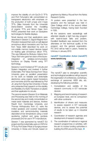
08010 Barcelona, Spain. responsible for cracks as differential thermal
expansion at material interfaces is not
manageable.
Abstract > Heat management in today’s A key parameter in the improvement of the
electronic devices is critical to prevent device design is therefore the understanding
possible failures due particularly to cracks. of heat conduction in the devices. Here
Heat is carried in such devices by electrons we focus on one way to measure the
in electrical conductors and mainly by implications of the particle behaviour (mean
acoustic phonons in electrical insulators. free path) of acoustic phonons when they
We explain the first steps of our work are confined in tiny structures. We propose a
aiming to investigate experimentally the method to analyse the heat flux propagation
effect of lateral confinement of acoustic in these structures and show our first efforts
phonons in silicon ridges as a function of towards the efficient use of the designed
the temperature. Inspired by the electrical samples.
3ω method, we design a setup that can be
used as a mean to generate phonons in 2. Heat flux measurements in low-
~100 nm wide ridge nanostructures and dimensional samples
as a thermometer that allows tracking the
generated heat flux. A. The macroscopic 3ω method
The 3ω method has been developed since
1. Introduction the 1980s, in particular by Cahill [3], with the
Works performed over the last decades goal of studying the thermal conductivity
have shown that electronic devices with of planar materials. Thin films have been
nanometre-scale dimensions are subject investigated widely as well as the thermal
to larger temperature-driven stresses in boundary resistance between the films [4].
comparison to what had been estimated in It was extended for multilayer materials or
the past [1]. In particular, the size of different particle-based materials [5, 6]. The method
components of transistors and electronics is based on the Joule heating of a metallic
devices present in printed circuits are now wire of micrometric size deposited on top of
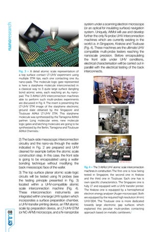
12 comparable to the key scales associated the substrate that “steals” part of the heat
13. nanoresearch
flux generated. As a consequence, the substrate thermal conductivity has to be
temperature of the wire gives an indication found. A 2D cross-section based model
on the ability of the sample to conduct heat. has been used extensively over the past
The use of a harmonic current to heat the 20 years. It is based on frequency sweeps.
wire allows the excitation of the temperature The slope of the temperature variation gives
higher-order harmonics. If the heating is not the thermal conductivity [3]. Some authors
too high, only the third harmonic is excited have underlined that better models can be
as will be seen in the following. One can used [7, 8]. Usually, the width of the wire is
write for a current I = I0 cos(ωt) the generated in the micrometric range, which is reached
power due to the Joule heating as with standard optical lithography in the
fabrication process.
P(t) = R I(t)2 = ½ R (1 + cos(2ωt))
and the total temperature reads including B. Implementation at the nanoscale
the heating TDC by DC current : The case of nanoelectronic devices is very
different to the micrometre-scale one. Even
T(t) = T0 + TDC + T2ω cos(2ωt+ 2ω). if the heating/sensing system that can be
The key point now is the dependence of used has the same principle, the sizes are
the wire resistivity to temperature, that is much smaller. We fabricated nanostructures
linear in first approximation for low heating: where the heater/sensor lies on top of silicon
R(T) = R0 (1+α ∆T). Finally, the voltage of the substrates as represented in Fig. 1. The top
wire can be written as of a ridge is a wire, either a metal or doped
silicon, which acts as a heater and as a
U = RI = R0I0 [1+α(TDC+T2ωcos(2ωt+ 2ω))] cos(ωt) thermometer at the same time. The doped-
= R0I0 [(1+αTDC) cos(ωt)+½αT2ωcos(ωt- 2ω) layer structure requires epitaxial growth of
+½αT2ωcos(3ωt+ doped silicon.
2ω)]
The use of a lock-in amplifier at the third
harmonic enables to measure the amplitude
and the phase of the third harmonic and thus
extract the local temperature. The amplitude
is U3ω = ½ αR0I0 T2ω. The frequency range
to be used here is generally between 10 and
5000 Hz. Care has to be taken with the wire
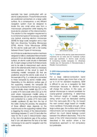
width and thickness that should be smaller Fig. 1 > Two types of resistive heater for the ridge
than the thermal diffusion wavelength in order experiments./
to prevent from a possible nonhomogeneity The substrates can be made of high-
of the heat generation in the wire. resistivity silicon. The submicrometer ridges
This experimental part of the work permits are fabricated with electron beam lithography
only to get a qualitative idea of the material and ICP dry etching (see Fig. 2, page 14).
thermal properties or to make an estimate This type of structure enables to generate
based on comparisons with reference phonons in the ridge and to measure the heat
materials the thermal conductivity of which is flux flowing to the substrate. An adaptation
known. This is not an easy task as a heating of the 3ω method is then used to heat the
device has to be deposited on top of each wire and measure the wire temperature. As
sample. it has been previously explained, a harmonic
If one wants to find the thermal conductivity electrical current generates the heat at 2ω
directly from the sample, a physical model due to Joule effect and lock-in detection
linking the measured temperature and the allows measuring the in-phase 3ω voltage 13
14. nanoresearch
(a) (b) in certain cases. The standard wire method
deals in general with a few Ohms.
Lithography
mask
3. Phonons in silicon and some size
effects
A. Silicon properties
Silicon is a semiconductor where electrons
(c) (d) are the charge carriers but most of the
heat is carried through phonons. The
thermal conductivity of pure silicon is
at room temperature,
which is high in comparison to amorphous
materials such as SiO2 with thermal
conductivities two orders of magnitude
below. Note that gold, one of the best
metallic heat conductors, is only conducting
heat two times better than silicon. Despite
this high thermal conductivity, it can be
shown with the Wiedemann-Franz law
Fig. 2 > Examples of the fabricated structures: (a)
Overall view of one layout (b) Zoom on a ridge
that the electronic contribution to thermal
with a metal wire before mask removal (c) Zoom conductivity is negligible even at moderate
on a ridge with a doped silicon layer showing a doping levels. The phononic thermal
nonrectangular shape after reactive ion etching conductivity of a crystal can be written
(d) Connection between the measured wire and
electrical access./
component proportional to the wire 2ω
temperature. Note that one needs generally where the integration spans over the
to filter the spurious signal generated by frequency ω and the discrete sum over the
the source at 3ω. A 4 points measurement three different polarizations. is the reduced
is better usually, but 2 points can be also Planck constant; f is the Bose-Einstein
used in some cases. The difference with distribution; T the temperature; g is the
the macroscopic method is that a different phononic density of states; vg the phonon
physical model has to be used to link the mode group velocity; τ is the phonon
wire temperature to the heat flux transmitted relaxation time and (vg τ) is the phonon
to the substrate. mode mean free path. The high thermal
The first test is to measure the electrical conductivity is therefore due to either high
resistance of the device as a function of velocities, large density of states or large
the temperature, as varying this parameter phonons mean free path.
allows determining the value of the
temperature coefficient α needed for the B. Acoustic phonons, mean free paths
measurements. It can be found that α In general, mean free paths are parameters
is positive or negative depending on the that are not very-well known as they
temperature and the type of heater/sensor. (1) depend strongly on the frequency
The major experimental difference with the whereas they are generally calculated
macroscopic method is the value of the as an average and (2) are very difficult to
14 resistances that can be as high as 20 kΩ measure at room temperature. Some early
15. nanoresearch
measurements were reported in the 1960s reader to the mentioned references from
at lower temperature [9], and more recent the group of Goodson for the study of such
experiments using electrical methods [10] phenomena.
and time-domain thermoreflectance have
shown that part of the phonon mean free 4. Heat conduction in electric tracks and
path distribution should lie at lengths above ridges
500 nm. An alternative way to get insights In electronic devices with deposited metal
in the issue of mean free path is the use of lines or doped silicon tracks, the electronic
molecular dynamics simulation. Henry and path lies on top of planar substrates.
Chen [11] recently calculated a distribution Considering a phonon mean free path on
of the mean free paths for silicon, finding the order of 100 nm, we present in Fig. 3
indeed that around 30% of the thermal three types of possible devices that consist
conductivity was due to mean free paths of a ridge on a planar substrate of the same
larger than 1 micrometer. This is consistent or different material. For simplification, we
with the estimation [10] that the mean free start with only similar materials. The left
path should be around 300 nm for silicon. device can be treated with the usual Fourier
Here one should keep in mind that the heat conduction, the middle one is different
widespread evaluation of the mean free as even if the nanostructure on top is large
path vgτ from is delicate and is in a thermal equilibrium the thermal
in the sense that it counts all the optical constriction resistance to the cold bath has
modes in the specific heat cp, whereas they to be described by a subcontinuum heat
are not expected to play a key role in the conduction. The right device is even further
thermal conductivity due to the flatness of complicated as the size of the structure does
their dispersion relation (vg≈0). Here ρ is the not allow an equilibrium inside due to its small
material density as usual. This approximation size and the fact that phonons are not trapped
underestimates the effect of the phonon in the cavity but can also escape. The centre
rarefaction in small devices. Recent works figure is typical of the rarefaction effect [19],
performed with nanowires [12, 13, 14] and when the phonon statistics impinging the
with embedded nanoparticles [15, 16], constriction is different than the equilibrium
targeting thermal conductivity reduction one. The right one has been tackled in
in thermoelectric materials, have also a theoretical paper [20]. In principle, the
highlighted the effect of roughness [14, Boltzmann transport equation has to be used
15] in addition to the phonon-particle for calculating the heat flux in structures such
confinement effect. Here we do not discuss as the centre and right ones but approximate
the suspended wire issue as it is for the methods have been developed such as the
moment less relevant in nanoelectronics. ballistic-diffusive equation [21, 22].
We need also to underline the role of
the interaction of electrons and optical (a) (b) (c)
phonons with the acoustic ones [17, 18].
Even if optical phonons do not carry heat
significantly they interact with the acoustic
ones, therefore impacting the thermal
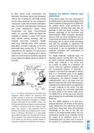
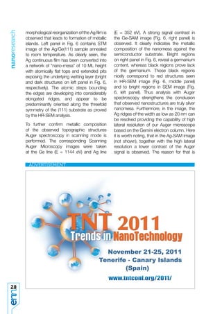
conductivity through the scattering mean
Fig. 3 > Three types of electrical conductors on a
free path. Note also that electron scattering
planar substrate. The substrate can be either an
with optical phonons is significant, and the electric conductor or an insulator. The Fourier
heat redistribution to acoustic phonons description of heat conduction is not adequate
takes place through optical/acoustic for the two last devices (b,c) if the phonon mean
phonons scattering interaction. We refer the free path is of the order of 100 nm or more./ 15
16. nanoresearch
Transient Heat Conduction Problems using
Ballistic-Diffusive Equations and Phonon
Boltzmann Equation”, Journal of Heat Transfer,
Vol. 127, pp.298-306 (2005).
[3] D. Cahill, “Thermal conductivity measurements
from 30 to 750 K: The 3ω method”, Review of
Scientific Instruments, Vol. 61, p802 (1990).
[4] S.-M. Lee and David G. Cahill, “Heat transport
in thin dielectric films,” Journal of Applied
Physics, Vol. 81, 2590 (1997).
[5] S.-M. Lee, David G. Cahill, and R.
Venkatasubramanian, “Thermal conductivity of
Si-Ge superlattices,” Applied Phyics. Letters,
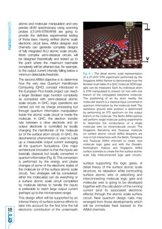
Fig. 4 > Different regimes of heat conduction as a Vol. 70, 2957 (1997).
function of the shape of the body in contact with [6] D.-A. Borca-Tasciuc and G. Chen, “Thermal
the substrate. Adapted from Ref [20]./ Properties of Nanochanneled Alumina
Templates,” Journal of Applied Physics, Vol.
The purpose of our work is to observe 79, pp. 084303-1-9 (2005).
these kinds of subcontinuum effects [7] T. Borca-Tasciuc, R. Kumar, and G. Chen,
experimentally. We have already measured “Data Reduction in 3ω Method for Thin Film
[23] the expected strong reduction of the Thermal Conductivity Measurements,” Review
thermal conductance in the ballistic regime of Scientific Instruments, Vol. 72, o. 4, pp.
with respect to Fourier’s prediction. Our 2139-2147 (2001).
first results indicate in addition a different [8] T. Tong and A. Majumdar, “Reexamining
behavior than what can be calculated in the the 3-omega technique for thin film thermal
purely ballistic case, which is exactly what characterization”, Review of Scientific
is pointed out in the analysis developed in Instruments, Vol. 77, 104902-104902-9 (2006).
Figs. 3 and 4. [9] R. Gereth and K. Hubner, “Phonon MeAn
Free Path in Silicon Between 77 and 250°K”,
Acknowledgements Physical Review, Vol. 134, pp A235–A240
(1964).
We thank M. Tilli for providing high ohmic
[10] M. Asheghi, Y.K. Leung, S.S. Wong, and K.E.
8” Si wafers. M. Myronov and V. Shah are
Goodson., “Phonon-Boundary Scattering in
acknowledged for doing the n+ Si epitaxial
Thin Silicon Layers,” Applied Physics Letters,
growth.
Vol. 71, pp. 1798-1800 (1007).
We acknowledge the partial support [11] A. Henry and G. Chen, “Spectral Phonon
of the EU projects NANOPACK and Properties of Silicon Based Molecular Dynamics
NANOPOWER. P.O.C. acknowledges the and Lattice Dynamics Simulations,” Journal of
support of EU project nanoICT for the partial Computational and Theoretical Nanosciences,
funding of a stay at VTT. Vol. 5, pp. 141-152 (2008).
[12] D. Li, Y. Wu, P. Kim, L. Shi, P. Yang, A.
References Majumdar, “Thermal conductivity of individual
[1] D.G. Cahill, W. K. Ford, K.E. Goodson, G.D. silicon nanowires,” Applied Physics Letters, Vol.
Mahan, A. Majumdar, H.J. Maris, R. Merlin, and 83, pp. 2934-2936 (2003).
S.R. Phillpot, “Nanoscale thermal transport,” [13] A. I. Hochbaum, R. K. Chen, R. D. Delgado,
Applied Physics Reviews, Journal of Applied W. J. Liang, E. C. Garnett, M. Najarian, A.
Physics, Vol. 93, p793 (2003). Majumdar, P.D. Yang. “Enhanced thermoelectric
[2] R.G. Yang, G. Chen, M. Laroche, and Y. Taur, performance of rough silicon nanowires,”
16 “Simulation of Nanoscale Multidimensional Nature, Vol. 451, pp. 163-167 (2008).
17. nanoresearch
[14] I. Akram Boukai, Y. Bunimovich, J. Tahir-Kheli, Phonon Dispersion,” Journal of Applied
J.-K. Yu, W.A. Goddard III, and J.R. Heath, Physics, Vol. 96, no. 9, pp. 4998-5005 (2004).
“Silicon nanowires as efficient thermoelectric [19] G. Chen, G. Chen, “Nonlocal and
materials”, Nature, Vol. 451, pp168-171 (2008). Nonequilibrium Heat Conduction in the Vicinity
[15] W. Kim, J. Zide, A. Gossard, D. Klenov, S. of Nanoparticles,” ASME Journal of Heat
Stemmer, A. Shakouri, A. Majumdar, “Thermal Transfer, Vol. 118, pp. 539-545 (1006).
conductivity reduction and thermoelectric figure [20] S. Volz and P.-O. Chapuis, “Increase of thermal
of merit increase by embedding nanoparticles resistance between a nanostructure and a
surface due to phonon multireflections”, Journal
in crystalline semiconductors,” Physical Review
of Applied Physics, Vol. 103(3), p034306 (2008).
Letters, Vol. 96, p045901 (2006).
[21] G. Chen, “Ballistic-Diffusive Heat Conduction
[16] W. Kim, S. L. Singer, A. Majumdar, J. M. O.
Equations,” Physical Review Letters, Vol. 85,
Zide, D. Klenov, A. C. Gossard, S. Stemmer,
pp. 2297-2300 (2001).
“Reducing thermal conductivity of crystalline
[22] G. Chen, “Ballistic-Diffusive Equations for
solids at high temperature using embedded
Transient Heat Conduction from Nano to
nanostructures,” Nano Letters, Vol. 8, pp.
Macroscales”, Journal of Heat Transfer, Vol.
2097-2099 (2008). 124, pp. 320-328 (2002).
[17] S. Sinha, E. Pop, R.W. Dutton, K.E. Goodson, [23] P.O. Chapuis, M. Prunnila, A. Shchepetov, L.
“Non-Equilibrium Phonon Distributions in Sub- Schneider, S. Laakso, J. Ahopelto, and C.M.
100 nm Silicon Transistors,” ASME Journal of Sotomayor, “Effect of phonon confinement
Heat Transfer, Vol. 128, pp. 638-647 (2006). on heat dissipation in ridges”, Proceedings of
[18] E. Pop, B. Dutton, and K.E. Goodson, “Analytic the 16th International Worshop on THERMal
Band Monte Carlo Model for Electron Transport INvestigations of ICs and Systems (THERMINIC),
Modeling in Si Including Acoustic and Optical B. Courtois and M. Rencz (ed), (2010).
17
18. nanojobs
• PostDoctoral Position (CEA-Léti, We are looking for talented chemists
France): ”Theory and modeling of NEMS motivated to pursue a PhD in the area of
based digital functions” Materials Science. The students will be
CMOS technology scaling has enabled able to join to a pioneer, dynamic and
significantly reduced energy per operation active group from the Department of
in integrated circuits. However, these NanoScience and Organic Materials (www.
improvements are not in line with the icmab.es/nmmo). This research group
expected performances of future approaches some of the most exciting
and challenging fields that a chemist and
autonomous systems. Autonomous
a materials scientist can explore nowadays
systems that use energy harvesting are
— the study of advanced organic functional
attractive for many applications (medical
materials and nanoscopic systems with
implants, micro-sensors, internet of things
useful electronic (superconductors, metallic
devices…). Today technologies used in conductors, semiconductors), magnetic
autonomous systems are not efficient (ferromagnets, superparamagnets, single
enough for ultra low power applications. The molecule magnets, nanoporous magnets,
transistor threshold voltage has been scaled etc), biological and/or optical properties.
to optimally balance leakage and dynamic We also involved on the development of
power but optimized performances are materials processing techniques, molecular
below autonomous systems specifications. self-assembly and on the preparation of
The deadline for submitting applications functional nanostructured materials.
is October 13, 2011 The deadline for submitting applications
For further information about the position, is October 15, 2011
please contact: For further information about the position,
Hervé Fanet (herve.fanet@cea.fr) please contact:
Jaume Veciana (vecianaj@icmab.es)
• PostDoctoral Position (CEA-Léti,
France): ”Characterization of a flexible array • PhD Position (IMM - CSIC, Spain):
of tactile sensors” ”New paradigms and New Devices based
We aim to develop a flexible tactile sensor on Nanomechanics”
based on MEMS technology developed The aim of this PhD project is the
at CEA Léti. Three-axis force sensors development of new NEMS devices and
developed at Léti and already tested for new sensing paradigms to achieve the
texture measurements will be integrated in ultimate limits in biological detection based
an array. The work proposed will include on nanomechanics. Silicon nanowires
both the integration and characterization of together carbon nanotubes represent
the flexible sensor array. the ultimate limit in the minituarization of
The deadline for submitting applications nanomechanical resonators. It is expected
is October 13, 2011 that these devices can be applied for
ultrasensitive mass sensing at the sub-
For further information about the position, zeptogram level and for mass spectroscopy
please contact: of single biomolecules. However, the
Caroline Coutier achievement of the optimal performance
(caroline.coutier@cea.fr) of these devices requires a detailed
understanding of the nanomechanical
• PhD Position (ICMAB - CSIC, Spain): response and a major development of the
“Functionalisation of surfaces with optical instrumentation for the detection of
functional organic molecules for electronic the picometer scale vibrations. In this PhD
18 or biological applications” project advanced optical instrumentation
19. nanojobs
and modeling of the nanomechanical and Group and ETSF Scientific Development
optical response of the silicon nanowires Centre in Spain and the Theory group of
will be developed. Finite element simulations the Fritz-Haber-Institut in Berlin. The aim
and analytical models will be developed in of the research project is to develop new
order to describe how the static and dynamic concepts for understanding, identifying,
response of nanomechanical systems with and quantifying the different contributions
different geometries behaves when subject to energy harvesting and storage as well as
to biological adsorption. The final aim will be describing transport mechanisms in natural
to establish the potential for weighing single light harvesting complexes, photovoltaic
biomolecules and measuring molecular materials, fluorescent proteins and artificial
recognition at the level of few events. (nanostructured) devices by means of
The deadline for submitting applications theories of open quantum systems, non-
is October 18, 2011 equilibrium processes and electronic
For further information about the position, structure.
please contact: The deadline for submitting applications
Montserrat Calleja is October 31, 2011
(mcalleja@imm.cnm.csic.es) For further information about the position,
please contact:
• PostDoctoral Position (ICFO, Spain):
”Optics and Photonics” Angel Rubio (Angel.Rubio@ehu.es)
ICFO – The Institute of Photonic Sciences is • PostDoctoral Position (CEA-Léti,
a center based in Castelldefels (Barcelona), France): ”CMOS electro-optical bridge for
Spain, devoted to the research and network-on-chip and optical network”
education of the optical and photonic
sciences, at the highest international level. The forecasted developments of high-
No restrictions of citizenship apply to the performance computing (HPC) and
ICFO post-doctoral contracts. Candidates Cloud computing induce new needs for
must hold an internationally-recognized computation density and data mining. The
PhD-equivalent degree in a field of science architectural model is built from a large
and engineering related to optics and number of processors sharing a huge
photonics. Suitable backgrounds include memory (eventually several terabytes).
optics, physics, mathematics, electronics Besides, while networks-on-chip (NoC) are
and telecommunications engineering. becoming the dominant interconnection
The deadline for submitting applications paradigm within chips, the connections to
is October 20, 2011 large memories are still point-to-point. The
For further information about the position, gap between the theoretical computing
please contact: power and the effective or real computing
Ariadna García power is hence widening because of
(ariadnag@heuristica.org) bandwidth limitations to shared memory
and increasing communication latency.
• Postdoctoral and PhD positions Emerging high-bandwidth connection
(University of the Basque Country UPV/ standards (DDR3, WideIO…) remain
EHU, Spain): ”Dynamical processes in incremental solutions and do not allow
Open Quantum Systems” concurrent accesses to a large number of
Applications are invited for postdoctoral and memory banks.
PhD positions link to a five year project on The deadline for submitting applications
the topic of Dynamical processes in open is October 31, 2011
quantum systems as part of an European
Research Council Advanced grant (DYNamo For further information about the position,
project). The project will be conducted please contact:
between the NanoBio Spectroscopy Yvain Thonnart (yvain.thonnart@cea.fr) 19
20. www.nanociencia.imdea.org
RESEARCH PROGRAMMES
• Molecular nanoscience
IMDEA-Nanociencia is a private Foundation created by joint initia-
tive of the Comunidad de Madrid and the Ministry of Education of
• Scanning probe microscopies the Government of Spain in February 2007 to manage a new
and surfaces
research Institute in Nanoscience and Nanotechnology (IMDEA-
Nanociencia). The Institute is located at the campus of the Univer-
• Nanomagnetism sidad Autónoma de Madrid in Cantoblanco.
The Institute aims at performing research of excellence in selected
• Nanobiosystems: biomachines and
manipulation of macromolecules areas and offers attractive opportunities to develop a career in sci-
ence at various levels from Ph.D. students to senior staff positions.
• Nanoelectronics and
superconductivity The Madrid Institute for Advanced Studies in Nanoscience also
develops an important program of technology transfer and creation
of spin-off companies.
• Semiconducting nanostructures
and nanophotonics
E-mail contacto.nanociencia@imdea.org
Phone 34 91 497 68 49 / 68 51
Fax 34 91 497 68 55
• Nanofabrication and advanced
instrumentation
[Nanociencia y Nanotecnología: lo pequeño es diferente small is different
Nanoscience and Nanotechnology:
]
21. nanoICT Conf Report
7th International Thin Film Transistor
Conference-ITC 2011
3-4 March 2011, Clare College, Cambridge
Organisers were presentations on CNTs and nanowires
W.I.Milne > Engineering Dept, University of for use in TFTs. In terms of distribution, an
Cambridge, UK. equal balance in presentations was achieved
Arokia Nathan > Electrical & Electronic Engineering
University College, London, UK.
between materials and applications, fulfilling
www-g.eng.cam.ac.uk/edm/itc2011/ the primary theme of ITC2011.
Much of the meeting concentrated on the
Sponsored by:
production, characterisation and application
of metal oxide based semiconductors
although there were also several reports on
the use of organic based material systems for
TFTs. Metal Oxide transistors are becoming
increasingly important as their mobility is
much higher than those of amorphous
The aim of this meeting was to highlight
silicon based TFTs and, as their stability
the on-going work on Thin Film Transistors
is improved, their use in practical systems
(TFTs), including a-Si:H and related materials
including flat panel displays, sensors and
systems such as nano, micro and poly
LEDs cannot be far away.
crystalline silicon. Sessions however also
included work on metal oxides, organics, There were 7 oral sessions and a poster
semiconducting nanowires, carbon session on both afternoons. The first session
nanotubes (CNTs) and naturally the new was based on Materials & Processing
“material of choice” graphene. Thin-film and the invited papers in this session were
Transistors (TFTs) have become increasingly presented by Hiroshi Tanabe from NEC
important since amorphous silicon (a-Si:H) and Richard Wilson from CDT. Dr Tanabe’s
TFTs were first incorporated in the backplanes presentation was on TFT technologies for
in AMLCD TVs. They of course are now being Flexible Displays based on the production
considered for a variety of other applications of metal oxide TFTs at low temperatures
including RFID tags, sensors, smart tags, using an excimer laser annealing technique.
etc. and increasingly in flexible electronics. Richard Wilson’s talk concentrated on
However the electronic properties of a-Si:H solution processing of organic TFTs with field
limit its possible applications and a variety effect mobilities in excess of 1 cm2V-1 cm-2.
of different material systems are now being The optimisation of the solvent selection
investigated as alternatives. from which the material is deposited is key to
This year the conference theme was on enhancing and controlling crystalline domain
Novel Materials, Processing and Device- formation.
Circuit Integration. There were 110 abstracts Session 2 and 8 concentrated on Thin Film
submitted and 150 attendees many from the Transistors themselves and the invited talks
Far East. here were given by Kenji Nomura from Tokyo
There were 17 invited speakers and 29 Tech and Elvira Fortunato from FCT-UNL,
contributed papers who presented their work Portugal. In his presentation Prof Nomura
on a variety of thin film material systems. There described the work they have been doing to 21
22. nanoICTConfReport
improve the stability of a-In-Ga-Zn-O TFTs graphene by Markuu Rouval from the Nokia
and Prof Fortunato’s talk concentrated on Research Centre.
transparent electronics with emphasis on 74 posters were presented in the two
the production of both p-type and n-type sessions and the banquet was held in
TFTs. Gilles Horowitz from the Université
Clare College which is the second oldest
Denis-Diderot covered the modelling
Cambridge College, having been founded
of organic TFTs and Simon Ogier from
in 1326.
PeTEC presented their work on backplane
technologies for flexible displays. All the sessions were exceedingly well
attended despite a tight two-day program
Novel devices and their applications were
described in Session 3. Sigurd Wagner from with back-to-back talks and posters.
Princeton reviewed their work on self aligned Excellent feedback was received from the
amorphous silicon transistors and Yue Kuo attendees on the technical quality of the
from Texas A&M described his work on program and the general organization.
non-volatile memory based devices based ITC 2012 will be held in Lisbon, hosted by
on floating gate amorphous silicon TFTs. Uninova, in January 2012.
This was followed by Mutsuku Hatano from
Tokyo Tech who gave her vision of the future- nanoICT Coordination Action (nanoICT)
integration of wireless-communication www.nanoict.org
functions on Display Panels using TFT
technology.
Sessions 4 and 6 looked at TFT circuits and
System Integration and involved 4 further
invited talks. Prof Takao Someya from Tokyo
The nanoICT plan to strengthen scientific
University gave an excellent presentation
and technological excellence will go beyond
on his work on foldable and stretchable
the organisation of conferences, workshops,
electronics using organic based transistors
exchange of personnel, WEB site, etc.
and memories and this was followed by Prof
developing the following activities:
Jin Jang from Kyung Hee University in Korea
who presented their research on the stability 1. Consolidation and visibility of the
and flexibility of a-IGZO Transistors on plastic research community in ICT nanoscale
and their application to circuits. devices
The second session (Session 5) on Materials 2. Mapping and benchmarking of research
and Processing was held on the morning of at European level, and its comparison
the second day and mostly concentrated on with other continents
metal oxide materials and devices. Andrew 3. Identification of drivers and measures
Flewitt from Cambridge University and to assess research in ICT nanoscale
Thomas Anthopoulos from I.C. were the
devices, and to assess the potential
invited speakers and covered respectively
of results to be taken up in industrial
insulators and semiconducting materials
research
deposited at low temperature using a novel
sputtering method and spray pyrolysis 4. Coordination of research agendas and
processed ZnO for use in TFT manufacture. development of research roadmaps
Session 7 was sponsored by nanoICT EU 5. The coordination of national or regional
project and the invited talks were on CNTs for research programmes or activities, with
TFTs by Prof Didier Pribat of Sungkyunkwan the aim to involve funding authorities in
22 University in Korea and Circuits based on building the ERA around this topic.
23. nanoresearch
The raise up of UHV atomic scale
interconnection machines
J. S. Prauzner-Bechcicki1, D. Martrou2,
C. Troadec3, S. Gauthier2, M. Szymonski1 and
C. Joachim2,3
1Center for nanometer-Scale Science and Advanced
Materials (NANOSAM), Faculty of Physics,
Astronomy and Applied Computer Science
Jagiellonian University, Reymonta 4, Krakow, Poland.
2Centre d’Elaboration de Matériaux et d’Etudes Fig. 1 > A single five wings molecule-motor [1]
Structurales (CEMES-CNRS), 29, rue Jeanne Marvig, positioned between a 4 Au nano pads junction
BP 94347, 31055 Toulouse Cedex 4, France. constructed at the Si(100)-H surface. The 4 black
3Institute of Materials Research and Engineering,
wires getting out of the surface are indicative of the
A*STAR (Agency for Science, Technology and interconnections step 3 discussed in the text depending
Research), 3 Research Link, Singapore 117602. on the electronic gap of the supporting surface./
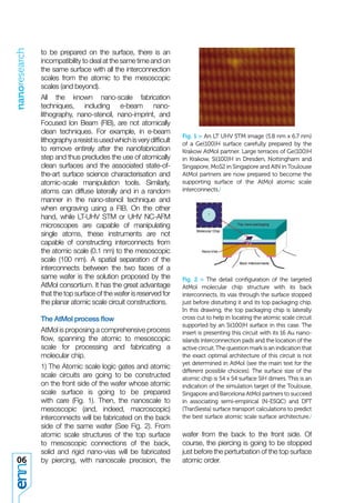
1. Introduction In section 2, the general principles of the
Single molecule mechanics [1], mono- few UHV atomic scale interconnection
molecular electronics [2] and surface machines under test to solve the problem are
atomic scale circuits [3] [4] are all requiring a described. Depending on the electronic gap
specific surface interconnection technology of the surface where the atomic scale devices
with an atomic precision and cleanness and machineries are supposed to work, two
[5]. In a planar configuration, this surface families of interconnections machines are
technology must be able to provide multiple being explored. Section 3 is providing one
access electronic channels to the atomic (or example of an atomic scale interconnection
molecular) scale machinery constructed on a machine designed for the surface of wide
surface (see for example Fig. 1). At the end gap semi-conductor and insulator materials.
of the 80’s, it was expected that the e-beam Section 4 is giving the example of two
nano-lithography technique would be able interconnection machines for moderate gap
to provide such a technology [6]. But with its semi-conductor surfaces. The design and
resist based approach, e-beam technique instrumentation works reported here are
will not face the challenge [7] because it is the consequence of the EU ICT integrated
not able to respect at the same time the project Pico-Inside in Krakow and Toulouse
atomic scale precision, the cleanness and together with the A*STAR VIP Atom Tech
the expected large number N of access Phase 2 project in Singapore. It is now further
channels to the atomic scale machinery developed in the new EU ICT integrated
[8]. Alternative nanolithography techniques project AtMol and in the Phase 3 of the
such as nano-imprint [9] or nano-stencil A*STAR VIP Atom Tech project in Singapore.
[10] are neither adapted to encompass
all the interconnection stages from the 2. Atomically precise electrical
macroscopic to the atomic scale nor clean interconnection machine
enough down to the atomic scale. At the turn An atomic scale precision, multiple access,
of the century, this problem triggers a new electrical interconnection instrument must
approach to planar electrical interconnects provide N conducting wires converging
starting from the bottom that is from the toward a very small surface area where
fundamentals of surface science. an active machinery (see Fig. 1 for a N=4 23
24. example) has been constructed with an
atomic scale precision. Those N interconnects
are positioned somewhere on a large wafer
surface. As a consequence, a very efficient
navigation system must be designed to
locate this very small active area from a
macroscopic perspective while keeping the
local atomic precision of the interconnection.
The solution to this navigation requirement is
to combine two types of microscopy: a far field
one (optical, scanning electron microscope
(SEM)) for large scale navigation and a near
field one (Scanning Tunneling Microscope
(STM), Atomic Force Microscope (AFM))
for the atomic scale part with a full overlay
between those 2 types of microscopy.
An UHV atomic scale interconnection machine is
Fig. 2 > Scheme of the atomic scale interconnection
designed to follow a dedicated interconnection machines for (a) wide and (b) moderate surface
protocol. On an atomically clean well-prepared band gap substrates. A: Atomic scale circuitry,
surface, an atomic scale circuitry is fabricated B: Contacting metallic nanopads, C1: Ultrasharp
(A). To reach a large number N of interconnects metallic tips, C2: Nanowires, D: Microelectrodes, E:
and to be able to interconnect each atomic Metallic microcantilevers./
wire to the external world, there is a necessary
lateral extension of this circuit to reach N
3. UHV interconnection machine for large
contacting metallic nanopads (B) that are
surface gap
positioned around the atomic scale circuit. In
the example of Fig. 2, a molecule is connected For a large valence-conduction band
to these nanopads by atomic metallic wires. electronic surface gap (more than a few eV
Depending on the electronic surface gap of up to 8 eV for standard insulators), SEM
the supporting material, the nanopads (B) is difficult to use as a navigation far field
have to be contacted from the top by a series microscope because its electron beam
of N atomically sharp metallic tips (C1) or by will charge the surface. In this case, an
a series of N nano-scale wires (C2) up to the optical microscope is natural candidate for
point where mesoscopic metallic wiring or coarse-grained positioning. It determines
microelectrodes (D) can be surface fabricated the minimum length of metallic surface
and contacted by a series of N micro-scale wiring which must be fabricated starting
metallic cantilevers (E) also from the top of from the nano-pads (B) in Fig. 2a toward
the wafer. During the process, the sequence the next contact stage based on metallic
of those different steps depends on the micro-cantilever. Fortunately enough, with a
machine and on the supporting material. What large surface gap, the surface area of those
is triggering the choice of the interconnection interconnects can be expanded horizontally
technology between C1 and C2 (and after the without too much lateral leakage current
need for the D and E interconnection steps between the different electrodes. This is the
in Fig. 2a) is the electronic gap of the surface basis of the UHV interconnection machine
that in turn will determine the kind of far field described in this section where a low
microscopy to be used for navigation over the temperature approach is not compulsory
24 wafer surface. but preferable.
25. nanoresearch
To realize the 5 levels of interconnect 1. a flexural-hinge guided (XY) nano-
described in Fig. 2a in UHV, the deposition positioner stage (100 μm x 100 μm,
of molecules, their observation by NC-AFM repeatability 5 nm) with a closed loop
and the measurement of their electrical control based on capacitive sensors,
properties, the Toulouse group has designed 2. an evaporation system highly collimated
and constructed a dedicated UHV equipment on the cantilever to perform nano-stencil
called DUF (DiNaMo UHV Factory). This deposition,
equipment allows transferring samples under
UHV between five complementary UHV 3. a (XYZ) piezo driven table for positioning
chambers (see Fig. 3): the metallic micro-combs for the
electrical contacts,
(1) an MBE growth chamber dedicated
to nitride semiconductors growth, 4. an optical microscope to control the
metallic nano-pads growth and stencil positioning of the micro-combs.
evaporation for microelectrodes These modifications were introduced by
(2) a room temperature AFM/STM chamber the mechanical workshop of the Toulouse
for surface characterization by STM and laboratory. The main advantage of using
NC AFM a commercial UHV AFM/STM is to benefit
from the good characteristics for SPM
(3) an AFM/STM chamber modified for
imaging. But the piezo tube used to scan
nano-stenciling experiments and
has a range of a few μm only. The addition of
electrical measurements
a piezo table to move the sample offers the
(4) a preparation chamber for cleaning possibility to perform wide range scanning,
substrates, STM tips and AFM cantilevers up to 80 μm SPM images, while keeping the
(5) a mass spectrometer chamber possibility to realize atomic sale imaging with
transformed in a molecular ions source. the piezo tube.
For (3) a UHV Omicron Nanotechnology One of the disadvantages is the small
VT STM/AFM head has been modified to accessible space around the SPM head.
accommodate different tools, namely [11]: Indeed, it is not possible to place an optical
Fig. 3 > The DUF (DiNaMo UHV Factory) equipment allows to transfer samples between 5
complementary UHV chambers in order to realize the 5 levels of interconnect on wide band gap
semiconductors (GaN, AlN)./ 25
26. nanoresearch
microscope with normal incidence with Krakow and the other in Singapore. The
respect of the substrate, and an atomic Krakow’s system consists of three basic
source for the nano-stencil experiments with segments: multi-probe, low-temperature
normal incidence with respect to the AFM scanning probe microscope (LT-SPM)
cantilever. In our case, the image obtained and preparation chambers. Multi-probe
by the optical microscope comes from a segment is composed of 4-probe scanning
mirror with an angle of 30° with the substrate tunnelling microscope (STM) combined
plane. This gives distorted images, with with high resolution scanning electron
a loss of resolution: only 3 μm instead of microscope (HR-SEM) and hemispherical
1 μm in normal incidence. The effusion cell electron energy analyser (scanning Auger
is fixed on a port of the UHV chamber that microscope, SAM) (see Fig. 4). The Auger
makes an angle of 33° with the horizontal microscope part is the element not present
plane, and another angle of 28° between in Singapore’s setups. Composition of the
the two vertical planes passing through the multi-probe segment allows surface element
evaporation beam and the central axis of analysis, imaging and measurements of
the cantilever. This orientation of the atom nanostructures conductance with very
beam induces distortion, which should be high-resolution. In accord with the Fig. 2b
taken into account in the design of the nano- principle, HR-SEM may act as a navigation
pattern to be drilled into the pyramidal tip of to precisely position each of the 4 STM tips
the cantilever [11].
(a)
4. UHV interconnection machine for
moderate semi-conductor surface gap
For a moderated valence band-conduction
band electronic surface gap (around a few
eV), it is not possible to use very long surface
metallic circuitry due to the possible lateral
surface leakage current between the surface
electrodes. In this case, one solution is to
use ultra sharp STM like tips positioned from
the top on the surface as microelectrodes
(Fig. 2b). In this case, the core of the tips will (b)
not be in contact with the supporting surface
and one can go continuously from a tip apex
radius of curvature of a few nanometer up
to a 100 microns or more section for the
tip body. In this case, navigation on the
surface can be performed using an UHV-
SEM (Fig. 2b) by grounding the sample
during the SEM imaging to avoid the surface
charging effect. This is the basics of the
UHV interconnection machines described
here. A low temperature approach is
compulsory with those systems because of Fig. 4 > (a) View on sample stage of 4-probe
the low electronic gap at the surface of the microscope; in upper part one can see SEM
column and next to it an entrance to hemispherical
supporting material.
electron energy analyser; below SEM column
There are two apparatuses that realize the there are three of four STM probes. (b) SEM image
26 above described design, one is housed in of four STM probes./
27. nanoresearch
that will be used as microelectrodes. First
measurements of conductance of gold
nanostructures on Ge(001) surface are in
progress.
Next, LT-SPM segment consist of scanning
probe microscope that may work both as
STM and NC-AFM in a range of temperatures
Fig. 5 > InSb surface imaged with q-sensor NC-
from 4K up to room temperature. Thanks AFM in temperature 4K./
to use of scanner and sample holder
embedded in a cryostat, the LT-UHV STM
SAM images of metallic nano-mesa grown
allows for a very high resolution imaging, as
on semiconductor substrate are shown.
well as, stable spectroscopic measurements
The Ag/Ge(111) is an example of a system
and atomic scale manipulations.
for which depending on the deposition
Furthermore, NC-AFM mode is based on conditions, on the successive thermal
q-sensor device (tuning fork) that enables annealing and on the amount of deposited
imaging of conducting, semiconducting and material the resulting overlayer morphology
insulating samples at low temperatures (see can be switched from an atomically smooth
Fig. 5) and, if required, also simultaneous to a columnar-like [12]. Sample is prepared in
measurements of tunnelling current. This the following way: silver in amount of nominal
option makes the Krakow’s system a very 5 ML is deposited on the germanium surface
powerful tool. Last but not least, is the kept at low temperature. Low energy electron
preparation segment that consist of typical diffraction studies performed immediately
preparation equipment such as a XYZ after deposition reveal that compact silver
manipulator with electric contact allowing for film is crated. Such a conclusion follows from
resistive heating up to 1000K (using a direct the fact that reflections characteristic for
heating mode 1200K may be achieved), the unreconstructed Ag(111) overlayer are
furthermore the manipulator allows for observed exclusively on LEED image. One
cooling the sample down to 100K with may assume it is a clear and direct indication
nitrogen vapour, an ion gun, a low energy that Ge substrate is completely buried.
electron diffraction system for quick sample In the next step the sample is annealed to
quality tests and several ports allowing room temperature. After annealing a massive
for incorporation of additional elements
(for instance effusion cells or quartz
microbalance thickness monitor) into the
chamber. All segments are composed of the
highest quality elements all of them being
compatible to work in UHV environment
(less than 3×10⁻¹⁰mbar), and thus allowing
Fig. 6 > STM, HR-SEM and SAM images of the Ag/
for conducting very complex experiments Ge(111) sample. Image size: 220nm × 270nm. Left
in a single set-up in a very controlled panel: STM image; Middle panel: HR-SEM image;
way, starting from sophisticated sample Right panel: SAM image. STM image reveals bright
preparation and ending with extensive and nanostructures 2.5nm high. The same regions
complete characterisation. are marked red in HR-SEM image. In SAM image
those structures are black. SAM image was taken
As the Auger microscopic part of the
for Ge line (E=1144 eV), thus exposing as bright
Krakow’s nano-probe instrument is not regions containing Ge. Therefore, it is possible to
present in the other setups (see above and identify the black structures in SAM image (bright
below) its potential is briefly described in the and red regions on STM and HR-SEM images,
following. In Fig. 6, the STM, HR-SEM and respectively) as silver islands./ 27