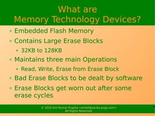
Embedded Storage
  Management


© 2010 Anil Kumar Pugalia <email@sarika-pugs.com>
               All Rights Reserved.
What to Expect?
W's of Memory Technology Devices
MTD Subsystem
MTD related Drivers
Flash File Systems
Flash Tools


        © 2010 Anil Kumar Pugalia <email@sarika-pugs.com>   2
                       All Rights Reserved.
Storage Timeline
Traditionally (for most of past 20+ years)
  ROM – For read-only storage
  NVRAM – For read-write storage
Equating with today's technology
  Low-density
  Costlier
Latest trend is flash technology devices
  More commonly referred as MTD
  Comes as NOR, NAND, some exotic varieties
  Best suited for Embedded Systems
             © 2010 Anil Kumar Pugalia <email@sarika-pugs.com>   3
                            All Rights Reserved.
What are
Memory Technology Devices?
Embedded Flash Memory
Contains Large Erase Blocks
  32KB to 128KB
Maintains three main Operations
  Read, Write, Erase from Erase Block
Bad Erase Blocks to be dealt by software
Erase Blocks get worn out after some
erase cycles
         © 2010 Anil Kumar Pugalia <email@sarika-pugs.com>   4
                        All Rights Reserved.
NOR Flash
Reading like RAM
 Random Access
 Execute Code (XIP)
 Could be replacement for ROM (but slower)
Manufacturers
 Intel, AMD, Fujitsu and Toshiba
Capacity
 Typically from a few KBs to 64MB

        © 2010 Anil Kumar Pugalia <email@sarika-pugs.com>   5
                       All Rights Reserved.
NAND Flash
Reading like Hard Disk
  Multiples of 512 bytes at a time
  No XIP
Higher Density & Cheaper than NOR
Highly prone to errors at the bit level
  Needs software to handle bad blocks
Manufacturers: Samsung and Toshiba
Capacity: Typically from 8MB to 1024MB. Today,
even more
           © 2010 Anil Kumar Pugalia <email@sarika-pugs.com>   6
                          All Rights Reserved.
Writing into Flash
Same for both NOR and NAND Flash
Sequence of Steps needed
Almost always involve an erase cycle
As Writing of Data means
  Flipping a bit to "0" or leaving it as a "1"
  Flipping a bit to "1" needs an erase cycle


         © 2010 Anil Kumar Pugalia <email@sarika-pugs.com>   7
                        All Rights Reserved.
MTD Subsystem
                  File I/O                        Raw I/O, MTD Utils
                                                                 User Space
                VFS Layer                                        Kernel Space


Individual File Systems


  mtdblock, FTL, NFTL           mtdchar            JFFS2    YAFFS2


                                MTD Core                                 MTD Layer
NAND Chip
 Drivers
                 NOR Chip Drivers
                                                   Map Drivers
                   (CFI, JEDEC)
                             Probe
                                                                 Hardware Space
                                            I/O
  NAND                   NOR
            © 2010 Anil Kumar Pugalia <email@sarika-pugs.com>                        8
                           All Rights Reserved.
Map Drivers
Drivers to Map
  Flash Memory Range for CPU access
  Mark the Storage Partitions in the Kernel
       As no partition table on flash
       Shows up as /dev/mtd*
Example
  Browse the drivers/mtd/maps/ folder
Data Structures
  struct mtd_partition (Header: <linux/mtd/partitions.h>)
  struct map_info (Header: <linux/mtd/map.h>)
Header: <linux/mtd/mtd.h>
APIs
  int add_mtd_partitions(struct mtd_info *, const struct mtd_partition *, int);
  int del_mtd_partitions(struct mtd_info *);
                     © 2010 Anil Kumar Pugalia <email@sarika-pugs.com>            9
                                    All Rights Reserved.
NOR Chip Drivers
NOR Chip Drivers
  CFI specification
  JEDEC specification
CFI Command Sets
  0x01 – Intel & Sharp flash chips
  0x02 – AMD & Fujitsu flash chips
  0x03 – ST flash chips
All three are configurable in kernel

         © 2010 Anil Kumar Pugalia <email@sarika-pugs.com>   10
                        All Rights Reserved.
NAND Chip Drivers
Drivers for NAND Controller to access NAND
Sources: drivers/mtd/nand/
A NAND Drive should do the following
  Add an entry to nand_flash_ids[] in drivers/mtd/nand/nand_ids.c
  Entries being
    Id Name, Device Id, Page Size, Erase Block Size, Chip Size, Options like
    Bus Width, …
  As, no automatic configuration support
  Specify its out-of-band (OOB) spare area layout through the
  “struct nand_ecclayout” (Header: <mtd/mtd-abi.h>)
    For ECCs, to implement error correction & detection
  Enable Error Management, in case NAND Controller doesn't do it
    Software ECC is implemented in drivers/mtd/nand/nand_ecc.c
               © 2010 Anil Kumar Pugalia <email@sarika-pugs.com>               11
                              All Rights Reserved.
Kernel Configurations for MTD
CONFIG_MTD should be enabled
And whatever required under it, should be
enabled, e.g.
  Required NAND Driver, Or
  Required NOR Protocol
  etc


        © 2010 Anil Kumar Pugalia <email@sarika-pugs.com>   12
                       All Rights Reserved.
File Systems for Flash
Typical Requirements
  Flash wear-levelling
  Less Writes / Erases
  Protect Data during Erase Cycles
  Bad Block Management (esp for NAND)
  Possibly compression (though preferred on read-only
  file systems only)
File Systems handling these
  JFFS2 (log-structured design & garbage collection)
  YAFFS2 (specifically designed for NAND constraints)

           © 2010 Anil Kumar Pugalia <email@sarika-pugs.com>   13
                          All Rights Reserved.
Flash Tools
Useful tools to work with MTD layer
  flash_erase, flash_eraseall
  flash_lock, flash_unlock
  nanddump, nandwrite
  sumtool
  ...
Download from ftp://ftp.infradead.org/pub/mtd-utils
Tool to construct a JFFS2 file system image
  mkfs.jffs2

            © 2010 Anil Kumar Pugalia <email@sarika-pugs.com>   14
                           All Rights Reserved.
What all have we learnt?
W's of Memory Technology Devices
  About NOR & NAND
MTD Subsystem
MTD related Drivers
  Map, NOR Chip, NAND Chip
Flash File Systems
Flash Tools

        © 2010 Anil Kumar Pugalia <email@sarika-pugs.com>   15
                       All Rights Reserved.
Any Queries?


© 2010 Anil Kumar Pugalia <email@sarika-pugs.com>   16
               All Rights Reserved.

Embedded Storage Management

  • 1.
    Embedded Storage Management © 2010 Anil Kumar Pugalia <email@sarika-pugs.com> All Rights Reserved.
  • 2.
    What to Expect? W'sof Memory Technology Devices MTD Subsystem MTD related Drivers Flash File Systems Flash Tools © 2010 Anil Kumar Pugalia <email@sarika-pugs.com> 2 All Rights Reserved.
  • 3.
    Storage Timeline Traditionally (formost of past 20+ years) ROM – For read-only storage NVRAM – For read-write storage Equating with today's technology Low-density Costlier Latest trend is flash technology devices More commonly referred as MTD Comes as NOR, NAND, some exotic varieties Best suited for Embedded Systems © 2010 Anil Kumar Pugalia <email@sarika-pugs.com> 3 All Rights Reserved.
  • 4.
    What are Memory TechnologyDevices? Embedded Flash Memory Contains Large Erase Blocks 32KB to 128KB Maintains three main Operations Read, Write, Erase from Erase Block Bad Erase Blocks to be dealt by software Erase Blocks get worn out after some erase cycles © 2010 Anil Kumar Pugalia <email@sarika-pugs.com> 4 All Rights Reserved.
  • 5.
    NOR Flash Reading likeRAM Random Access Execute Code (XIP) Could be replacement for ROM (but slower) Manufacturers Intel, AMD, Fujitsu and Toshiba Capacity Typically from a few KBs to 64MB © 2010 Anil Kumar Pugalia <email@sarika-pugs.com> 5 All Rights Reserved.
  • 6.
    NAND Flash Reading likeHard Disk Multiples of 512 bytes at a time No XIP Higher Density & Cheaper than NOR Highly prone to errors at the bit level Needs software to handle bad blocks Manufacturers: Samsung and Toshiba Capacity: Typically from 8MB to 1024MB. Today, even more © 2010 Anil Kumar Pugalia <email@sarika-pugs.com> 6 All Rights Reserved.
  • 7.
    Writing into Flash Samefor both NOR and NAND Flash Sequence of Steps needed Almost always involve an erase cycle As Writing of Data means Flipping a bit to "0" or leaving it as a "1" Flipping a bit to "1" needs an erase cycle © 2010 Anil Kumar Pugalia <email@sarika-pugs.com> 7 All Rights Reserved.
  • 8.
    MTD Subsystem File I/O Raw I/O, MTD Utils User Space VFS Layer Kernel Space Individual File Systems mtdblock, FTL, NFTL mtdchar JFFS2 YAFFS2 MTD Core MTD Layer NAND Chip Drivers NOR Chip Drivers Map Drivers (CFI, JEDEC) Probe Hardware Space I/O NAND NOR © 2010 Anil Kumar Pugalia <email@sarika-pugs.com> 8 All Rights Reserved.
  • 9.
    Map Drivers Drivers toMap Flash Memory Range for CPU access Mark the Storage Partitions in the Kernel As no partition table on flash Shows up as /dev/mtd* Example Browse the drivers/mtd/maps/ folder Data Structures struct mtd_partition (Header: <linux/mtd/partitions.h>) struct map_info (Header: <linux/mtd/map.h>) Header: <linux/mtd/mtd.h> APIs int add_mtd_partitions(struct mtd_info *, const struct mtd_partition *, int); int del_mtd_partitions(struct mtd_info *); © 2010 Anil Kumar Pugalia <email@sarika-pugs.com> 9 All Rights Reserved.
  • 10.
    NOR Chip Drivers NORChip Drivers CFI specification JEDEC specification CFI Command Sets 0x01 – Intel & Sharp flash chips 0x02 – AMD & Fujitsu flash chips 0x03 – ST flash chips All three are configurable in kernel © 2010 Anil Kumar Pugalia <email@sarika-pugs.com> 10 All Rights Reserved.
  • 11.
    NAND Chip Drivers Driversfor NAND Controller to access NAND Sources: drivers/mtd/nand/ A NAND Drive should do the following Add an entry to nand_flash_ids[] in drivers/mtd/nand/nand_ids.c Entries being Id Name, Device Id, Page Size, Erase Block Size, Chip Size, Options like Bus Width, … As, no automatic configuration support Specify its out-of-band (OOB) spare area layout through the “struct nand_ecclayout” (Header: <mtd/mtd-abi.h>) For ECCs, to implement error correction & detection Enable Error Management, in case NAND Controller doesn't do it Software ECC is implemented in drivers/mtd/nand/nand_ecc.c © 2010 Anil Kumar Pugalia <email@sarika-pugs.com> 11 All Rights Reserved.
  • 12.
    Kernel Configurations forMTD CONFIG_MTD should be enabled And whatever required under it, should be enabled, e.g. Required NAND Driver, Or Required NOR Protocol etc © 2010 Anil Kumar Pugalia <email@sarika-pugs.com> 12 All Rights Reserved.
  • 13.
    File Systems forFlash Typical Requirements Flash wear-levelling Less Writes / Erases Protect Data during Erase Cycles Bad Block Management (esp for NAND) Possibly compression (though preferred on read-only file systems only) File Systems handling these JFFS2 (log-structured design & garbage collection) YAFFS2 (specifically designed for NAND constraints) © 2010 Anil Kumar Pugalia <email@sarika-pugs.com> 13 All Rights Reserved.
  • 14.
    Flash Tools Useful toolsto work with MTD layer flash_erase, flash_eraseall flash_lock, flash_unlock nanddump, nandwrite sumtool ... Download from ftp://ftp.infradead.org/pub/mtd-utils Tool to construct a JFFS2 file system image mkfs.jffs2 © 2010 Anil Kumar Pugalia <email@sarika-pugs.com> 14 All Rights Reserved.
  • 15.
    What all havewe learnt? W's of Memory Technology Devices About NOR & NAND MTD Subsystem MTD related Drivers Map, NOR Chip, NAND Chip Flash File Systems Flash Tools © 2010 Anil Kumar Pugalia <email@sarika-pugs.com> 15 All Rights Reserved.
  • 16.
    Any Queries? © 2010Anil Kumar Pugalia <email@sarika-pugs.com> 16 All Rights Reserved.