
Download to read offline

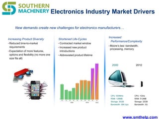
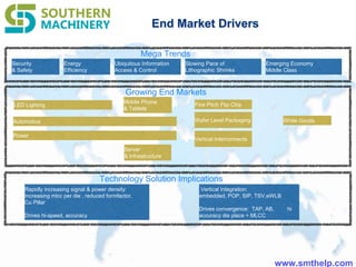
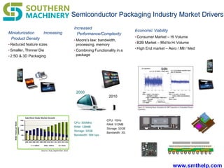
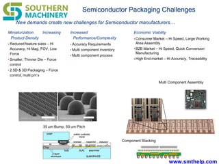


The document outlines the drivers and challenges in the electronics and semiconductor packaging industries, highlighting trends such as miniaturization, increased product complexity, and evolving consumer demands. It discusses the implications of technological advancements, including the performance impacts of Moore's Law and the need for economic viability in various markets. Additionally, it addresses the shift towards globalized manufacturing processes and advanced automation solutions to adapt to these market changes.


![ASIC Design Solution & Challenges for Shorter TTM [Infographic]](https://cdn.slidesharecdn.com/ss_thumbnails/asic-design-solutions-for-faster-ttm-171110060018-thumbnail.jpg?width=640&height=640&fit=bounds)


