DSP Architectures
Professor S.Srinivasan
Electrical Engineering Department
I.I.T.-Madras, Chennai –600 036
srini@ee.iitm.ac.in
2.
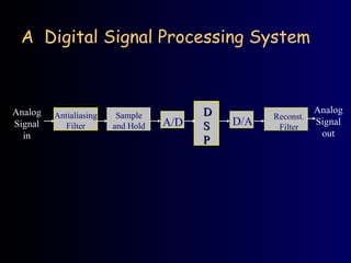
A Digital SignalProcessing System
Analog
Signal
in
Analog
Signal
out
Antialiasing
Filter
Sample
and Hold A/D
D
D
S
S
P
P
D/A Reconst.
Filter
3.
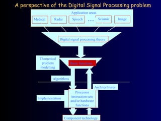
A perspective ofthe Digital Signal Processing problem
Application areas
Radar Speech Seismic Image
Medical • • •
Digital signal processing theory
Basic functions
Processor
instruction sets
and/or hardware
functions
Component technology
Theoretical
problem
modelling
Algorithms
Implementation
Architechtures
4.
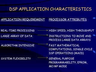
DSP APPLICATION CHARACTERISTICS
APPLICATIONREQUIREMENT PROCESSOR ATTRIBUTES
REAL-TIME PROCESSING HIGH SPEED, HIGH THROUGHPUT
LARGE ARRAY OF DATA INSTRUCTIONS TO MOVE AND
PROCESS LARGE DATA ARRAYS
ALGORITHM INTENSIVE FAST MATHEMATICAL
COMPUTATIONS, SINGLE CYCLE
DSP OPERATIONS (MACD)
SYSTEM FLEXIBILITY GENERAL PURPOSE
PROGRAMMABILITY, EPROM,
MC/MP MODE
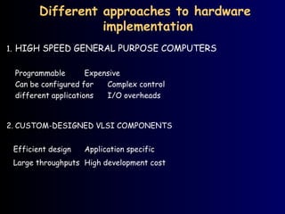
5.
Different approaches tohardware
implementation
1. HIGH SPEED GENERAL PURPOSE COMPUTERS
Programmable Expensive
Can be configured for Complex control
different applications I/O overheads
2. CUSTOM-DESIGNED VLSI COMPONENTS
Efficient design Application specific
Large throughputs High development cost
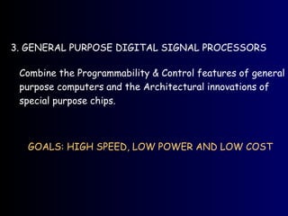
6.
3. GENERAL PURPOSEDIGITAL SIGNAL PROCESSORS
Combine the Programmability & Control features of general
purpose computers and the Architectural innovations of
special purpose chips.
GOALS: HIGH SPEED, LOW POWER AND LOW COST
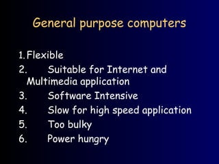
7.
General purpose computers
1.Flexible
2.Suitable for Internet and
Multimedia application
3. Software Intensive
4. Slow for high speed application
5. Too bulky
6. Power hungry
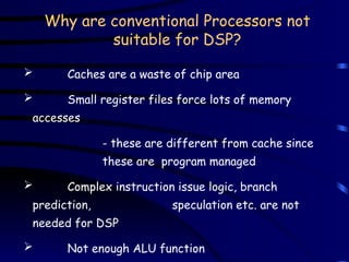
8.
Why are conventionalProcessors not
suitable for DSP?
Caches are a waste of chip area
Small register files force lots of memory
accesses
- these are different from cache since
these are program managed
Complex instruction issue logic, branch
prediction, speculation etc. are not
needed for DSP
Not enough ALU function
9.
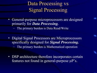
Data Processing vs
SignalProcessing
• General-purpose microprocessors are designed
primarily for Data Processing.
– The primary burden is Data Read/Write
• Digital Signal Processors are Microprocessors
specifically designed for Signal Processing.
– The primary burden is Mathematical operation
• DSP architecture therefore incorporates certain
features not found in general-purpose P’s.
10.
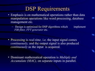
DSP Requirements
• Emphasisis on mathematical operations rather than data
manipulation operations like word processing, database
management etc.
– Design is optimized for DSP algorithms which implement
FIR filter, FFT generator etc.
• Processing is real-time, i.e. the input signal comes
continuously, and the output signal is also produced
continuously as the input is acquired.
• Dominant mathematical operation is Multiply and
Accumulate (MAC), on separate inputs in parallel.
11.
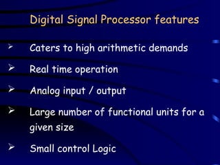
Digital Signal Processorfeatures
Caters to high arithmetic demands
Real time operation
Analog input / output
Large number of functional units for a
given size
Small control Logic
12.
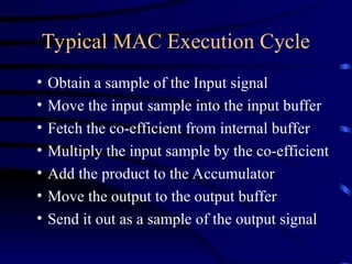
Typical MAC ExecutionCycle
• Obtain a sample of the Input signal
• Move the input sample into the input buffer
• Fetch the co-efficient from internal buffer
• Multiply the input sample by the co-efficient
• Add the product to the Accumulator
• Move the output to the output buffer
• Send it out as a sample of the output signal
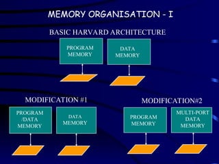
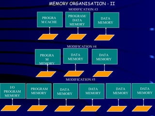
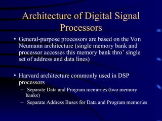
Architecture of DigitalSignal
Processors
• General-purpose processors are based on the Von
Neumann architecture (single memory bank and
processor accesses this memory bank thro’ single
set of address and data lines)
• Harvard architecture commonly used in DSP
processors
– Separate Data and Program memories (two memory
banks)
– Separate Address Buses for Data and Program memories
15.
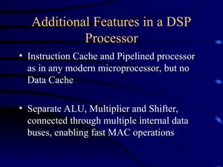
Additional Features ina DSP
Processor
• Instruction Cache and Pipelined processor
as in any modern microprocessor, but no
Data Cache
• Separate ALU, Multiplier and Shifter,
connected through multiple internal data
buses, enabling fast MAC operations
16.
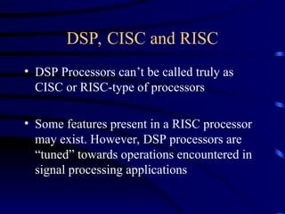
DSP, CISC andRISC
• DSP Processors can’t be called truly as
CISC or RISC-type of processors
• Some features present in a RISC processor
may exist. However, DSP processors are
“tuned” towards operations encountered in
signal processing applications
17.
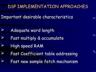
DSP IMPLEMENTATION APPROACHES
Importantdesirable characteristics
Adequate word length
Fast multiply & accumulate
High speed RAM
Fast Coefficient table addressing
Fast new sample fetch mechanism
18.
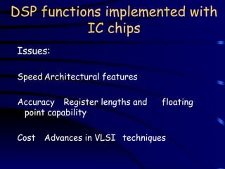
DSP functions implementedwith
IC chips
Issues:
Speed Architectural features
Accuracy Register lengths and floating
point capability
Cost Advances in VLSI techniques
19.
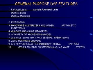
GENERAL PURPOSE DSPFEATURES
1. PARALLELISM: Multiple Functional Units
Multiple Buses
Multiple Memories
2. PIPELINING
3. HARDWARE MULTIPLIERS AND OTHER ARITHMETIC
FUNCTIONS
4. ON-CHIP AND CACHE MEMORIES
5. A VARIETY OF ADDRESSING MODES
7. INSTRUCTIONS THAT PACK SEVERAL OPERATIONS
8. ZERO-OVERHEAD LOOPING
9. I/O FEATURES SUCH AS INTERRUPT, SERIAL I/O, DMA
10. OTHER CONTROL FUNCTIONS SUCH AS WAIT STATES
20.
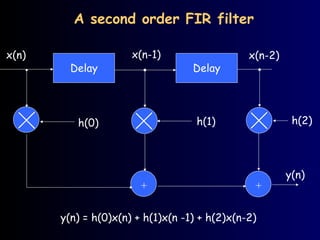
Delay Delay
x(n) x(n-2)
h(1)h(2)
y(n)
+ +
A second order FIR filter
h(0)
x(n-1)
y(n) = h(0)x(n) + h(1)x(n -1) + h(2)x(n-2)
21.
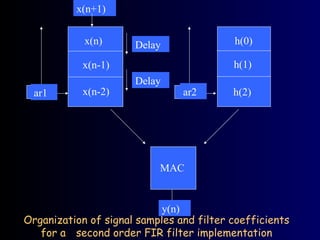
Organization of signalsamples and filter coefficients
for a second order FIR filter implementation
x(n+1)
y(n)
x(n)
x(n-1)
x(n-2)
h(0)
h(1)
h(2)
Delay
Delay
MAC
ar2
ar1
22.
An Nth
order FIRfilter implementation
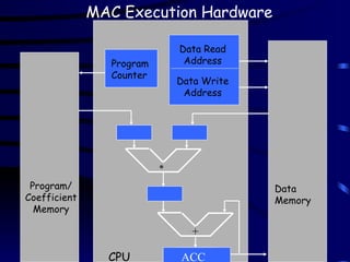
A[0]
A[1]
A[2]
• •
• •
• •
A[N-1]
Coefficient
Memory
*
+
X[n]
X[n-1]
X[n-2]
• •
• •
• •
X[n-N+1]
Data
Memory
ACC y[n]
P
23.
FIR Filter pseudo-code
Loadloop count
Initialize coefficient and data addr regs
Zero Acc and P registers
LOOP: Pnew = A[i] . X[n-i]
Accnew = ACCold + Pold
Decrement coefficient and data addr regs
X[n-i] X[n-i-1] {for next iteration}
Decr loop count
BNZ LOOP
Acc Y[n]
24.
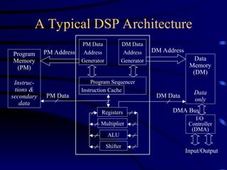
A Typical DSPArchitecture
Program
Memory
(PM)
Instruc-
tions &
secondary
data
Data
Memory
(DM)
Data
only
PM Data
Address
Generator
DM Data
Address
Generator
Program Sequencer
Instruction Cache
Registers
Multiplier
ALU
Shifter
I/O
Controller
(DMA)
PM Address DM Address
PM Data DM Data
Input/Output
DMA Bus
25.
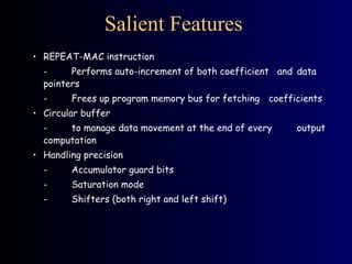
Salient Features
• REPEAT-MACinstruction
- Performs auto-increment of both coefficient and data
pointers
- Frees up program memory bus for fetching coefficients
• Circular buffer
- to manage data movement at the end of every output
computation
• Handling precision
- Accumulator guard bits
- Saturation mode
- Shifters (both right and left shift)
26.
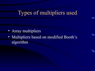
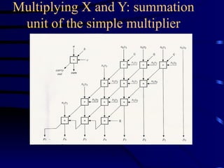
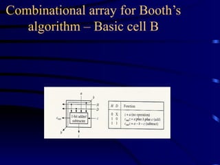
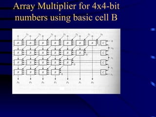
Types of multipliersused
• Array multipliers
• Multipliers based on modified Booth’s
algorithm
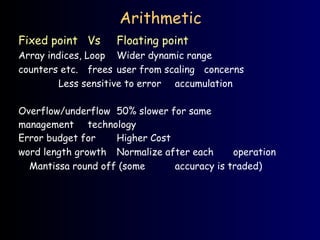
Arithmetic
Fixed point VsFloating point
Array indices, Loop Wider dynamic range
counters etc. frees user from scaling concerns
Less sensitive to error accumulation
Overflow/underflow 50% slower for same
management technology
Error budget for Higher Cost
word length growth Normalize after each operation
Mantissa round off (some accuracy is traded)
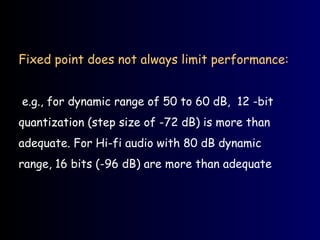
32.
Fixed point doesnot always limit performance:
e.g., for dynamic range of 50 to 60 dB, 12 -bit
quantization (step size of -72 dB) is more than
adequate. For Hi-fi audio with 80 dB dynamic
range, 16 bits (-96 dB) are more than adequate
33.
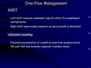
Overflow Management
SHIFT
Left shiftremoves redundant sign bit after 2’s complement
multiplication
Right shift down scales numbers as word growth is detected
Unbiased rounding
Prevents accumulation of a small dc bias from outputs which
fall just half way between adjacent rounded values
34.
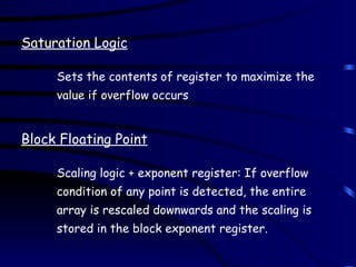
Saturation Logic
Sets thecontents of register to maximize the
value if overflow occurs
Block Floating Point
Scaling logic + exponent register: If overflow
condition of any point is detected, the entire
array is rescaled downwards and the scaling is
stored in the block exponent register.
35.
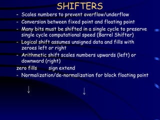
SHIFTERS
- Scales numbersto prevent overflow/underflow
- Conversion between fixed point and floating point
- Many bits must be shifted in a single cycle to preserve
single cycle computational speed (Barrel Shifter)
- Logical shift assumes unsigned data and fills with
zeroes left or right
- Arithmetic shift scales numbers upwards (left) or
downward (right)
zero fills sign extend
- Normalization/de-normalization for block floating point
36.
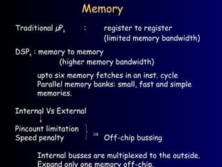
Memory
Traditional µPs :register to register
(limited memory bandwidth)
DSPs : memory to memory
(higher memory bandwidth)
upto six memory fetches in an inst. cycle
Parallel memory banks: small, fast and simple
memories.
Internal Vs External
Pincount limitation
Speed penalty Off-chip bussing
Internal busses are multiplexed to the outside.
Expand only one memory off-chip.
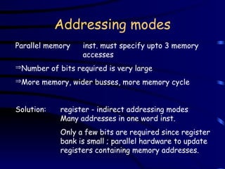
Addressing modes
Parallel memoryinst. must specify upto 3 memory
accesses
Number of bits required is very large
More memory, wider busses, more memory cycle
Solution: register - indirect addressing modes
Many addresses in one word inst.
Only a few bits are required since register
bank is small ; parallel hardware to update
registers containing memory addresses.
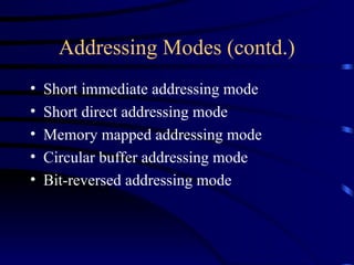
Instruction Level Parallelism
VLIWarchitecture
• Each instruction specifies several operations to
be done in parallel
• Advantages : Simple hardware
compilers can spot ILP
easily
• Disadvantages : Little compatibilty between
generations
Explicit NOPs bloat code
42.
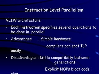
Super scalar architecture
•Hardware responsible for finding ILP in a
sequential program
• Advantage : Compatibility between
generations
• Disadvantage : Very complex hardware
43.
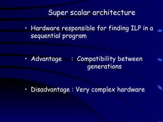
Explicitly Parallel InstructionComputing
(EPIC)
• Combines VLIW and super scalar
architectures
• Instructions are grouped into 3 operating
blocks and a template block
• Template block tells hardware if
instructions can be executed in parallel
• Also gives information whether the block
can be executed in parallel
44.
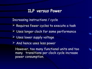
ILP versus Power
Increasinginstructions / cycle
Requires fewer cycles to execute a task
Uses longer clock for same performance
Uses lower supply voltage
And hence uses less power
However, too many functional units and too
many transitions per clock cycle increase
power consumption.
45.
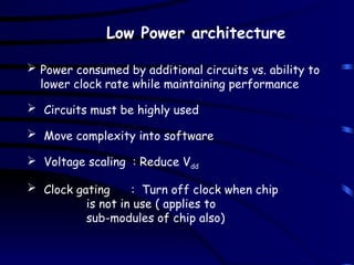
Low Power architecture
Power consumed by additional circuits vs. ability to
lower clock rate while maintaining performance
Circuits must be highly used
Move complexity into software
Voltage scaling : Reduce Vdd
Clock gating : Turn off clock when chip
is not in use ( applies to
sub-modules of chip also)
46.
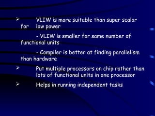
VLIW ismore suitable than super scalar
for low power
- VLIW is smaller for same number of
functional units
- Compiler is better at finding parallelism
than hardware
Put multiple processors on chip rather than
lots of functional units in one processor
Helps in running independent tasks
47.
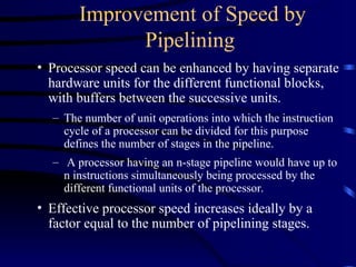
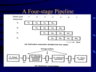
Improvement of Speedby
Pipelining
• Processor speed can be enhanced by having separate
hardware units for the different functional blocks,
with buffers between the successive units.
– The number of unit operations into which the instruction
cycle of a processor can be divided for this purpose
defines the number of stages in the pipeline.
– A processor having an n-stage pipeline would have up to
n instructions simultaneously being processed by the
different functional units of the processor.
• Effective processor speed increases ideally by a
factor equal to the number of pipelining stages.
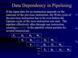
Data Dependency inPipelining
If the input data for an instruction depends on the
outcome of the previous instruction, the Write cycle of
the previous instruction has to be over before the
Operate cycle of the next instruction can start. The
pipeline effectively idles through one instruction,
creating a bubble in the pipeline which persists for
several instructions.
F4 D4
O3
F2 D2 idle W2
O2
W4
F3 idle D3 W3
O4
Bubble
ends
here
F1 D1 O1 W1
50.
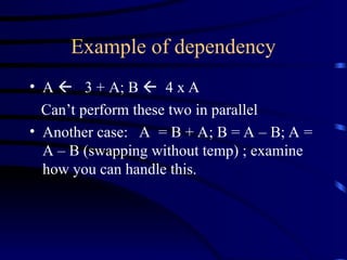
Example of dependency
•A 3 + A; B 4 x A
Can’t perform these two in parallel
• Another case: A = B + A; B = A – B; A =
A – B (swapping without temp) ; examine
how you can handle this.
51.
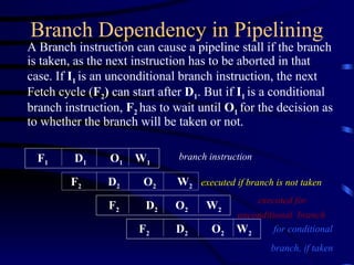
Branch Dependency inPipelining
A Branch instruction can cause a pipeline stall if the branch
is taken, as the next instruction has to be aborted in that
case. If I1 is an unconditional branch instruction, the next
Fetch cycle (F2) can start after D1. But if I1 is a conditional
branch instruction, F2 has to wait until O1 for the decision as
to whether the branch will be taken or not.
F1 D1 O1 W1
F2 D2 O2 W2 executed if branch is not taken
F2 D2 O2 W2
F2 D2 O2 W2
executed for
unconditional branch
for conditional
branch, if taken
branch instruction
52.
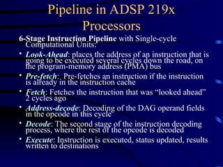
Pipeline in ADSP219x
Processors
6-Stage Instruction Pipeline with Single-cycle
Computational Units:
• Look-Ahead: places the address of an instruction that is
going to be executed several cycles down the road, on
the program-memory address (PMA) bus
• Pre-fetch: Pre-fetches an instruction if the instruction
is already in the instruction cache
• Fetch: Fetches the instruction that was “looked ahead”
2 cycles ago
• Address-decode: Decoding of the DAG operand fields
in the opcode in this cycle
• Decode: The second stage of the instruction decoding
process, where the rest of the opcode is decoded
• Execute: Instruction is executed, status updated, results
written to destinations
53.
Memory blockconflicts: If both instruction and data are to be
fetched from the same block of memory, a stall is
automatically inserted
DAG usage immediately (or within 2 cycles) after
initialization. e.g.
I2 = 0x1234;
AX0 = DM(I2,M2);
Bus conflicts: Instructions which use the PMA/PMD buses for
data transfer may cause bus conflict. e.g.
PM(I5,M7)=M3;
Causes for Pipeline Stalls
54.
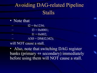
Avoiding DAG-related Pipeline
Stalls
•Note that
– I2 = 0x1234;
– I3 = 0x0001;
– I1 = 0x002;
– AX0 = DM(I2,M2);
will NOT cause a stall.
• Also, note that switching DAG register
banks (primary secondary) immediately
before using them will NOT cause a stall.
56.
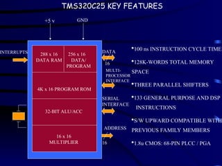
TMS320C25 KEY FEATURES
INTERRUPTS
+5v GND
288 x 16
DATA RAM
256 x 16
DATA/
PROGRAM
4K x 16 PROGRAM ROM
32-BIT ALU/ACC
16 x 16
MULTIPLIER
DATA
16
MULTI-
PROCESSOR
INTERFACE
SERIAL
INTERFACE
ADDRESS
16
100 ns INSTRUCTION CYCLE TIME
128K-WORDS TOTAL MEMORY
SPACE
THREE PARALLEL SHIFTERS
133 GENERAL PURPOSE AND DSP
INSTRUCTIONS
S/W UPWARD COMPATIBLE WITH
PREVIOUS FAMILY MEMBERS
1.8u CMOS: 68-PIN PLCC / PGA
57.
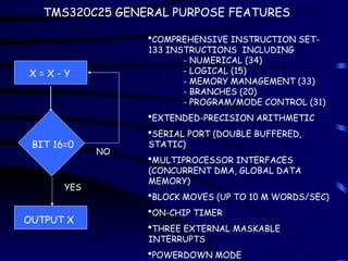
TMS320C25 GENERAL PURPOSEFEATURES
X = X - Y
BIT 16=0
OUTPUT X
NO
YES
COMPREHENSIVE INSTRUCTION SET-
133 INSTRUCTIONS INCLUDING
- NUMERICAL (34)
- LOGICAL (15)
- MEMORY MANAGEMENT (33)
- BRANCHES (20)
- PROGRAM/MODE CONTROL (31)
EXTENDED-PRECISION ARITHMETIC
SERIAL PORT (DOUBLE BUFFERED,
STATIC)
MULTIPROCESSOR INTERFACES
(CONCURRENT DMA, GLOBAL DATA
MEMORY)
BLOCK MOVES (UP TO 10 M WORDS/SEC)
ON-CHIP TIMER
THREE EXTERNAL MASKABLE
INTERRUPTS
POWERDOWN MODE
58.
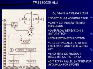
TMS320C25 ALU
DESIGN &OPERATION
32-BIT ALU & ACCUMULATOR
CARRY BIT FOR EXTENDED
PRECISION
OVERFLOW DETECTION &
SATURATION
SIGN EXTENSION OPTION
0-16 BIT PARALLEL SHIFTER
FOR LOADS AND ARITHMETIC
OPS
SHIFTERS ON PRODUCT
REGISTER OUTPUT DATA
0-7 BIT PARALLEL SHIFTER FOR
ACCUMULATOR STORES
59.
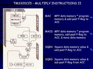
TMS320C25 - MULTIPLYINSTRUCTIONS II
MAC MPY data memory * program
memory & add past P-Reg to
ACC
MACD MPY data memory * program
memory, add past P-Reg to
ACC, & move data memory
SQRA Square data memory value &
add past P-Reg to ACC
SQRS Square data memory value &
sub past P-Reg from ACC
60.
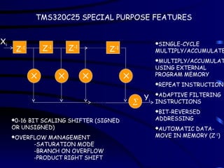
Xi
Yi
Z-1 Z-1 Z-1
Z-1
0-16BIT SCALING SHIFTER (SIGNED
OR UNSIGNED)
OVERFLOW MANAGEMENT
-SATURATION MODE
-BRANCH ON OVERFLOW
-PRODUCT RIGHT SHIFT
SINGLE-CYCLE
MULTIPLY/ACCUMULATE
MULTIPLY/ACCUMULAT
USING EXTERNAL
PROGRAM MEMORY
REPEAT INSTRUCTION
ADAPTIVE FILTERING
INSTRUCTIONS
BIT-REVERSED
ADDRESSING
AUTOMATIC DATA-
MOVE IN MEMORY (Z-1
)
TMS320C25 SPECIAL PURPOSE FEATURES
61.
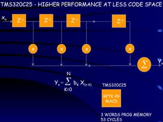
Z-1 Z-1
Z-1
Z-1
x xx x
xn
Yn
Yn = bK X(n-K)
N
K=0
TMS320C25
RPTK 49
MACD
3 WORDS PROG MEMORY
53 CYCLES
TMS320C25 - HIGHER PERFORMANCE AT LESS CODE SPACE
62.
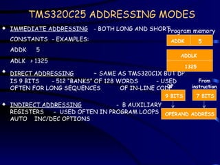
IMMEDIATE ADDRESSING- BOTH LONG AND SHORT
CONSTANTS - EXAMPLES:
ADDK 5
ADLK > 1325
DIRECT ADDRESSING - SAME AS TMS320C1X BUT DP
IS 9 BITS - 512 “BANKS” OF 128 WORDS - USED
OFTEN FOR LONG SEQUENCES OF IN-LINE CODE
INDIRECT ADDRESSING - B AUXILIARY
REGISTERS - USED OFTEN IN PROGRAM LOOPS WITH
AUTO INC/DEC OPTIONS
TMS320C25 ADDRESSING MODES
Program memory
ADDK 5
ADDLK
1325
9 BITS 7 BITS
OPERAND ADDRESS
DP
From
instruction
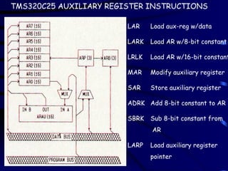
LAR Load aux-regw/data
LARK Load AR w/8-bit constant
LRLK Load AR w/16-bit constant
MAR Modify auxiliary register
SAR Store auxiliary register
ADRK Add 8-bit constant to AR
SBRK Sub 8-bit constant from
AR
LARP Load auxiliary register
pointer
TMS320C25 AUXILIARY REGISTER INSTRUCTIONS
65.
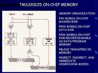
MEMORY ORGANIZATION
4K WORDSON-CHIP
MASKED ROM
544 WORDS ON-CHIP
DATA RAM
256 WORDS ON-CHIP
RAM RECONFIGURABLE
AS DATA/PROGRAM
MEMORY
BLOCK TRANSFERS IN
MEMORY
DIRECT, INDIRECT, AND
IMMEDIATE
ADDRESSING MODES
TMS320C25 ON-CHIP MEMORY
General-Purpose Microprocessor
circa 1984: Intel 8088
~100,000 transistors
Clock speed : ~ 5 MHz
Address space : 20 bits
Bus width : 8 bits
100+ instructions
2-35 cycles per instruction
Micro-coded architecture
68.
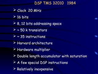
DSP TMS 320101984
Clock 20 MHz
16 bits
8, 12 bits addressing space
~ 50 k transistors
~ 35 instructions
Harvard architecture
Hardware multiplier
Double length accumulator with saturation
A few special DSP instructions
Relatively inexpensive
69.
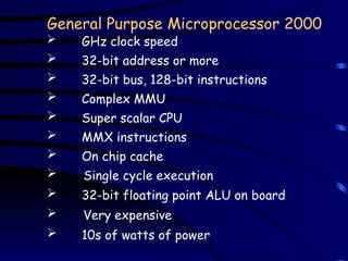
General Purpose Microprocessor2000
GHz clock speed
32-bit address or more
32-bit bus, 128-bit instructions
Complex MMU
Super scalar CPU
MMX instructions
On chip cache
Single cycle execution
32-bit floating point ALU on board
Very expensive
10s of watts of power
70.
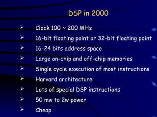
DSP in 2000
Clock 100 ~ 200 MHz
16-bit floating point or 32-bit floating point
16-24 bits address space
Large on-chip and off-chip memories
Single cycle execution of most instructions
Harvard architecture
Lots of special DSP instructions
50 mw to 2w power
Cheap
71.
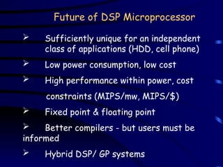
Future of DSPMicroprocessor
Sufficiently unique for an independent
class of applications (HDD, cell phone)
Low power consumption, low cost
High performance within power, cost
constraints (MIPS/mw, MIPS/$)
Fixed point & floating point
Better compilers - but users must be
informed
Hybrid DSP/ GP systems
Editor's Notes
#52 One of the biggest differences between the 21xx and the 219x is the instruction pipeline, which is now 6 deep. The most important thing to remember is that the pipeline has been designed in such a way as to be completely transparent from the standpoint of a user. In other words, the sequencer will automatically insert stalls where necessary, without the user having to install software stalls in their code.
The 219x instruction pipeline is 6-deep, consisting of the Look-ahead, the Pre-fetch, Fetch, Address-decode or Address-generation, Decode, and the Execute stages. Incorporated into the instruction pipeline is a 2-stage memory pipeline. What this essentially means is that at the operating speeds that the 219x is expected to run at, it is simply not possible to send out an address to memory and get the data back in the same cycle or the next cycle. If I send out an address to memory in a certain cycle, I can expect to get the corresponding data back from memory not in that cycle, or the next cycle, but two cycles down the road. It is important to remember this because the memory pipeline ties in closely to the 6-stage instruction pipeline.

![An Nth
order FIR filter implementation
A[0]
A[1]
A[2]
• •
• •
• •
A[N-1]
Coefficient
Memory
*
+
X[n]
X[n-1]
X[n-2]
• •
• •
• •
X[n-N+1]
Data
Memory
ACC y[n]
P](https://image.slidesharecdn.com/dsppresentationoverviewforclass-250909162649-3df2888e/85/DSP_presentation_overcview_for_class-ppt-22-320.jpg)
![FIR Filter pseudo-code
Load loop count
Initialize coefficient and data addr regs
Zero Acc and P registers
LOOP: Pnew = A[i] . X[n-i]
Accnew = ACCold + Pold
Decrement coefficient and data addr regs
X[n-i] X[n-i-1] {for next iteration}
Decr loop count
BNZ LOOP
Acc Y[n]](https://image.slidesharecdn.com/dsppresentationoverviewforclass-250909162649-3df2888e/85/DSP_presentation_overcview_for_class-ppt-23-320.jpg)