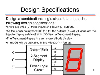
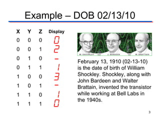
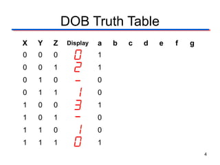
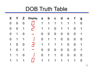
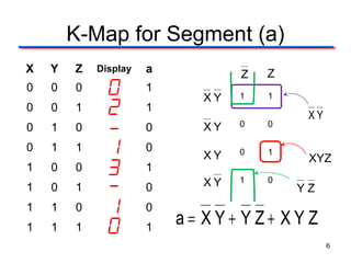
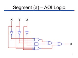
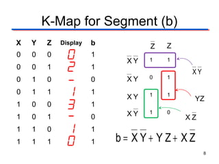
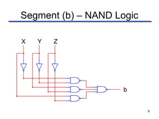
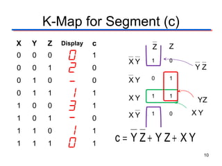
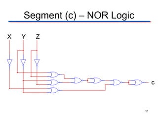
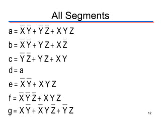
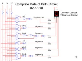
This document describes the design of a combinational logic circuit to display a date of birth on a 7-segment display. The circuit has 3 inputs (X, Y, Z) that will cycle through binary codes to represent dates. It drives 7 outputs (a-g) to control the display segments. Truth tables and K-maps are used to derive the logic expressions for each segment. The final circuit uses AOI, NAND and NOR gates to generate the correct segment outputs from the 3 inputs to display the date 02-13-10.
Evolving Balanced Maps for Planet Wars Using Self-Adaptive EAsCarlos Cotta
Paper presented at EvoGAMES 2013 (held within EvoStar 2013 in Vienna, Austria).
Procedural content generation (PCG) is the programmatic generation of game content using a random or pseudo-random process that results in an unpredictable range of possible gameplay spaces. This methodology brings many advantages to game developers, such as reduced memory consumption. This works presents a procedural balanced map generator for a real-time strategy game: Planet Wars. This generator uses an evolutionary strategy for generating and evolving maps and a tournament system for evaluating the quality of these maps in terms of their balance. We have run several experiments obtaining a set of playable and balanced maps
Solutions manual for digital logic and microprocessor design with interfacing...Brase947
Solutions Manual for Digital Logic and Microprocessor Design with Interfacing 2nd Edition by Hwang IBSN 9781305859456
Download at: https://goo.gl/SQyLGx
2. Design Specifications
Design a combinational logic circuit that meets the
following design specifications:
•There are three (3) three inputs and seven (7) outputs.
•As the inputs count from 000 to 111, the outputs (a – g) will generate the
logic to display a date of birth (DOB) on a 7-segment display.
•The 7-segment display is a common cathode display.
•The DOB will be displayed in the MM-DD-YY format.
a
Date of Birth
X b
7-Segment c
d
Y Display e
Driver Logic f
Z g
Circuit 2
3. Example – DOB 02/13/10
X Y Z Display
0 0 0
0 0 1
0 1 0
February 13, 1910 (02-13-10)
0 1 1 is the date of birth of William
1 0 0 Shockley. Shockley, along with
John Bardeen and Walter
1 0 1 Brattain, invented the transistor
1 1 0 while working at Bell Labs in
the 1940s.
1 1 1
3
4. DOB Truth Table
X Y Z Display a b c d e f g
0 0 0 1
0 0 1 1
0 1 0 0
0 1 1 0
1 0 0 1
1 0 1 0
1 1 0 0
1 1 1 1
4
5. DOB Truth Table
X Y Z Display a b c d e f g
0 0 0 1 1 1 1 1 1 0
0 0 1 1 1 0 1 1 0 1
0 1 0 0 0 0 0 0 0 1
0 1 1 0 1 1 0 0 0 0
1 0 0 1 1 1 1 0 0 1
1 0 1 0 0 0 0 0 0 1
1 1 0 0 1 1 0 0 0 0
1 1 1 1 1 1 1 1 1 0
5
6. K-Map for Segment (a)
X Y Z Display a Z Z
0 0 0 1
XY 1 1
0 0 1 1
XY
0 1 0 0 XY 0 0
0 1 1 0 0 1
XY XYZ
1 0 0 1
XY 1 0
1 0 1 0 YZ
1 1 0 0
1 1 1 1
a= XY+ YZ+ XYZ
6
12. All Segments
a= XY+ YZ+ XYZ
b= XY+ YZ+ XZ
c = YZ+ YZ+ XY
d= a
e= XY+ XYZ
f = XYZ+ XYZ
g= XY+ XYZ+ YZ 12
13. X Y Z
Complete Date of Birth Circuit
02-13-10
Common Cathode
7-Segment Display
AOI
Segment a & d
NAND Segment b
NOR Segment c
AOI
Segment e
NAND Segment f
NOR Segment g
13
Editor's Notes
Date of Birth Design Problem Digital Electronics 2.3 Date of Birth Design Problem Project Lead The Way, Inc. Copyright 2009
This slide contains the design specifications for the “Date of Birth” project. Date of Birth Design Problem Digital Electronics 2.3 Date of Birth Design Problem Project Lead The Way, Inc. Copyright 2009
This is an example of the “Date of Birth” problem using the birth date 02-13-10. http://web.mit.edu/invent/iow/shockleyetal.html Date of Birth Design Problem Digital Electronics 2.3 Date of Birth Design Problem Project Lead The Way, Inc. Copyright 2009
This is the truth table column for Segment (a). After reviewing how this truth table was developed, pause the presentation and allow the students to complete the truth table columns for segments (b) thru (g). The complete truth table is on the next slide. Date of Birth Design Problem Digital Electronics 2.3 Date of Birth Design Problem Project Lead The Way, Inc. Copyright 2009
This is the completed truth table. If you print handouts, do not print this page. Note that segment (a) & (d) are the same, thus you only need to design one circuit to be used for both segments. Date of Birth Design Problem Digital Electronics 2.3 Date of Birth Design Problem Project Lead The Way, Inc. Copyright 2009
This is the truth table column, its associated K-Map, & simplified logic expressions for segment (a). Date of Birth Design Problem Digital Electronics 2.3 Date of Birth Design Problem Project Lead The Way, Inc. Copyright 2009
This is logic diagram for segment (a). The circuit was implemented using AOI logic for demonstration purposes. It could have also been implemented with NAND or NOR logic. Date of Birth Design Problem Digital Electronics 2.3 Date of Birth Design Problem Project Lead The Way, Inc. Copyright 2009
This is the truth table column, its associated K-Map, & simplified logic expressions for segment (b). Note : In this example, the K-Map could have been grouped differently resulting in a different but equally simple logic expression (i.e., b = X’ Z + Y’ Z’ + X Y). Date of Birth Design Problem Digital Electronics 2.3 Date of Birth Design Problem Project Lead The Way, Inc. Copyright 2009
This is a logic diagram for segment (b). The circuit was implemented in NAND for demonstration purposes. It could also have been implemented with AOI or NOR logic. Date of Birth Design Problem Digital Electronics 2.3 Date of Birth Design Problem Project Lead The Way, Inc. Copyright 2009
This is the truth table column, its associated K-Map, & simplified logic expressions for segment (c). Note : Again, in this example, the K-Map could have been group differently resulting in a different but equally simple logic expression (i.e., b = Y’ Z’ + Y Z + X Z’). Date of Birth Design Problem Digital Electronics 2.3 Date of Birth Design Problem Project Lead The Way, Inc. Copyright 2009
This is a logic diagram for segment (c). The circuit was implemented in NOR for demonstration purposes. It could also have been implemented with AOI or NAND logic. Date of Birth Design Problem Digital Electronics 2.3 Date of Birth Design Problem Project Lead The Way, Inc. Copyright 2009
Here are all of the segments (a) – (g). Simplification and implementation of the segments (d) – (g) are left as an exercise that the students can complete as class work or homework. Date of Birth Design Problem Digital Electronics 2.3 Date of Birth Design Problem Project Lead The Way, Inc. Copyright 2009
This is the complete solution for the DOB problem for DOB 02-13-10. DON’T FORGET THE CURRENT LIMITING RESISTORS. The design will work in simulation without them, but if you build the circuit (i.e., in hardware) and do not include the resistors, the SSD will be destroyed. Date of Birth Design Problem Digital Electronics 2.3 Date of Birth Design Problem Project Lead The Way, Inc. Copyright 2009