SIMULATIONS AND PRACTICAL DESIGNS OF OFF.LINE CONVERTERS-THE FRONT ENDTsuyoshi Horigome
This document discusses different control methods for offline power factor correction (PFC) converters, including average current mode control, peak current mode control, and analytical control law methods. It then focuses on describing a borderline current mode PFC design that uses constant on-time control to achieve power factor correction. The converter senses the inductor current and uses a multiplier and error amplifier to impose a sinusoidally varying peak current setpoint that is proportional to the rectified input voltage, causing the input current to follow a sinusoidal envelope and correcting the power factor. The on-time is kept constant over a line cycle in borderline mode, resulting in frequency variations as the off-time changes to maintain a constant switching period.
- A new voltage-mode control scheme for buck converters improves performance at high frequencies by starting the ramp signal earlier, producing minimal jitter even at narrow duty cycles.
- Test results show the new scheme achieves jitter as low as 1.3ns at 1.5MHz switching frequency, compared to over 30ns for traditional control.
- The new scheme also enables monotonic start-up and allows higher bandwidth operation using fewer output capacitors.
Design and Simulation of PFC Circuit for AC/DC Converter Based on PWM Boost R...IOSR Journals
This document describes the design and simulation of a power factor correction (PFC) circuit for an AC/DC converter using a PWM boost regulator. Non-linear loads draw non-sinusoidal current from the power supply, reducing power quality. The proposed PFC circuit utilizes current shaping techniques with the boost inductor to generate a sinusoidal input current and improve the power factor. Simulation results showed the input current was sinusoidal in phase with the line voltage, achieving near unity power factor. Harmonic analysis revealed the 3rd, 17th, and 19th harmonics were significantly reduced after PFC, improving the power factor from 62.3% to 98.8%. The PFC circuit demonstrated effective mitigation of current harmon
This document discusses flyback converter design considerations for multi-kilowatt power conversion applications. It outlines flyback converter advantages and disadvantages, and solutions to overcome the disadvantages. Specifically, it focuses on single-stage power factor correction (PFC) applications using a flyback topology. The document discusses adapting the flyback converter for PFC, selecting an appropriate PFC control IC, modifying the control IC for high power applications, and transformer design considerations. It provides block diagrams and partial schematics as examples.
This paper presents the design of the feedback loop for single controller power factor correction converters. The feedback loop design must account for the large second harmonic component of the rectified input voltage. The size of the bulk capacitor and the corresponding loop gain affect the converter's performance in terms of total harmonic distortion, discontinuous conduction mode operation, and output regulation. The paper provides design procedures and examples for a boost-forward power factor correction converter. Simulation and experimental results validate the design approach.
The document provides an overview of National Semiconductor's LM315x Synchronous Simple Switcher® Controller Series. The controllers feature constant on-time control, wide input voltage range from 6V to 42V, adjustable output voltage down to 0.6V, and up to 95% peak efficiency. A simplified block diagram shows the basic hysteretic control scheme. Design examples demonstrate how to select components like MOSFETs, inductors, and capacitors to design a power supply circuit using the LM315x controllers. Evaluation boards are available to test designs with switching frequencies up to 1MHz and output currents up to 10A.
PID Controller Response to Set-Point Change in DC-DC Converter ControlIAES-IJPEDS
Power converter operations and efficiency is affected by variation in supply
voltage, loads current, circuit elements, ageing and temperature. To meet the
objective of tight voltage regulation, power converters circuit module and the
control unit must be robust to reject disturbances arising from supply, load
variation and changes in circuit elements. PID controller has been the most
widely used in power converter control. This paper presents studies of
robustness of PID controller tuning methods to step changes in the set point
and disturbance rejection in power converter control. A DC-DC boost
converter was modelled using averaged state-space mothod and PID
controllers were designed with five different tuning methods. The study
reveals the transient response and disturbance rejection capability of each
tuning methods for their suitability in power supply design applications.
The International Journal of Engineering & Science is aimed at providing a platform for researchers, engineers, scientists, or educators to publish their original research results, to exchange new ideas, to disseminate information in innovative designs, engineering experiences and technological skills. It is also the Journal's objective to promote engineering and technology education. All papers submitted to the Journal will be blind peer-reviewed. Only original articles will be published.
The papers for publication in The International Journal of Engineering& Science are selected through rigorous peer reviews to ensure originality, timeliness, relevance, and readability.
International Journal of Engineering Research and Applications (IJERA) is a team of researchers not publication services or private publications running the journals for monetary benefits, we are association of scientists and academia who focus only on supporting authors who want to publish their work. The articles published in our journal can be accessed online, all the articles will be archived for real time access.
Our journal system primarily aims to bring out the research talent and the works done by sciaentists, academia, engineers, practitioners, scholars, post graduate students of engineering and science. This journal aims to cover the scientific research in a broader sense and not publishing a niche area of research facilitating researchers from various verticals to publish their papers. It is also aimed to provide a platform for the researchers to publish in a shorter of time, enabling them to continue further All articles published are freely available to scientific researchers in the Government agencies,educators and the general public. We are taking serious efforts to promote our journal across the globe in various ways, we are sure that our journal will act as a scientific platform for all researchers to publish their works online.
Review of Step down Converter with Efficient ZVS OperationIJRST Journal
This paper presents the review of step down converter with efficient ZVS operation. The designed buck converter uses ZCS technique and the function is realized so that the power form is converted from 12V DC 5V DC (1A). A detailed analysis of zero current switching buck converters is performed and a mathematical analysis of the mode of operation is also presented. In order to reduce the switching losses in associated with conventional converters; resonant inductor and resonant capacitor (LC resonant circuit) is applied which helps to turn on-off the switch at zero current. The dc-dc buck converter receives the energy from the input source, when the switch is turned-on. The buck–buck converters have characteristics that warrant a more detailed study. The buck converters under discontinuous conduction mode /continuous conduction mode boundary.
Control ICs for Energy-efficient Fluorescent Ballast Applications Premier Farnell
The document describes the IRS2158D ballast control IC for fluorescent lighting applications. It provides an overview of the IC's functional blocks and operating states, including undervoltage lockout, preheat, ignition, pre-run and run modes. It also discusses dimming control, protection functions, and PCB layout considerations for using the IC in fluorescent electronic ballast designs.
This document summarizes two possible control techniques for indirectly shaping the input current of a buck power factor correction (PFC) converter by shaping the inductor current. It analyzes the harmonic content of the line current for each control technique to determine the allowable voltage gain (K value) for meeting various harmonic regulations. It then presents a sine-squared modulation control technique that shapes the average inductor current as a sine-squared waveform to indirectly shape the input current in a simplified manner without an averaging circuit. Simulation waveforms and equations are provided to analyze the line current harmonic distortion for different K values using this control technique. Experimental results from a 300W dual interleaved buck PFC converter are also mentioned.
This document summarizes a research paper that proposes a new Flipped Voltage Follower (FVF) low-dropout (LDO) voltage regulator using a Dual-Summed Miller Frequency Compensation (DSMFC) technique. The proposed LDO regulator can stabilize a load capacitance ranging from 10pF to 10nF using only 8pF of total compensation capacitance. Simulation results show the regulator maintains stability across the wide load capacitance range under varying load currents. The DSMFC technique improves stability compared to single Miller compensation, especially for large load capacitances with low load currents, large capacitances with moderate currents, and small capacitances with low currents. This allows the proposed regulator to
This paper addresses a novel approach for designing and modeling of the isolated
flyback converter. Modeling is done without parasitic as well as with parasitic components.
A detailed analysis, simulation and different control strategy are conferred for flyback
converter in continuous conduction mode (CCM). To verify the design and modeling at
primary stage, study of the converter is practiced in CCM operation for input AC voltage
230V at 50Hz and output DC voltage of 5V and 50W output power rating using PSIM 6.0
software. Simulation result shows a little ripple in output of the converter in open loop. Finally
in order to evaluate the system as well as response of the controller, flyback converter is
simulated using MATLAB. This work, highlighting the modeling when the system have
transformer and facilitate designers to go for it when they need one or more than one output
for a given application upto 150W
This document outlines the design of a 200 Watt, 150 Vrms PWM bipolar inverter with the following key points:
1. The design process includes calculating component values based on design requirements, building the circuit in Multisim software, and analyzing the simulation results.
2. Key calculations include determining the required DC bus voltage to achieve the 150Vrms AC output voltage despite voltage drops, as well as component sizing based on the given power, modulation index, and carrier frequency specifications.
3. Simulation results show the generated PWM switching signals and the final inverter output voltage matching the desired 150Vrms sinusoidal waveform.
Zero voltage switching resonant power conversionPham Hoang
The document summarizes the technique of zero voltage switching (ZVS) in power conversion. It explores several ZVS topologies and applications. It presents the benefits of ZVS which include lossless switching transitions, reduced switching losses, and ability to operate at high voltages and frequencies with high efficiency. The document then provides equations to analyze the voltage and current waveforms in a ZVS buck converter during the different intervals of the switching cycle. It analyzes the capacitor charging, resonant, and inductor charging states that occur between the switch turning off and back on. The analysis aims to understand how ZVS facilitates switching at zero voltage to reduce switching losses.
This document presents a design and simulation of a boost converter with input ripple cancellation for applications like fuel cells. It proposes a boost converter with a tapped inductor and ripple cancellation network (RCN) consisting of a small inductor and capacitor. This helps reduce input current ripples compared to a conventional boost converter. The RCN achieves input ripple cancellation by having its inductor current increase as the main inductor current decreases and vice versa. Simulation results show the proposed converter has lower input current ripple while maintaining output voltage regulation through a closed loop controller.
The document discusses improving the input power factor of a discontinuous conduction mode (DCM) buck power factor correction (PFC) converter. Normally, a buck PFC converter has a low input power factor due to its constant duty cycle over a line cycle and inherent dead zone. The paper proposes a variable duty cycle control scheme where the duty cycle is varied according to the rectified input voltage to make the input current proportional to the input voltage. This achieves near unity power factor. The duty cycle expression is simplified using Taylor series approximation to be implemented using analog control circuitry. Simulation results will verify this variable duty cycle control improves the input power factor compared to constant duty cycle control.
This document summarizes a research paper on an AC/DC converter with active power factor correction applied to a DC motor drive. The proposed circuit uses a quasi-active power factor correction technique with an auxiliary winding on a flyback converter transformer to shape the input current and improve the power factor. Simulation results are presented showing the performance of the circuit when applied to a DC motor load. The circuit aims to provide power factor correction without an active switch and control circuit to reduce costs and improve efficiency compared to traditional two-stage converter designs.
The document describes a positive trigger circuit using a 555 timer in monostable mode. In monostable mode, the 555 timer acts as a one-shot pulse generator that outputs a high pulse when the trigger pin is pulsed low. The width of the output pulse is determined by the RC time constant of the circuit. An LED is connected to the output to provide a visual indication of the pulse. The circuit was simulated and the timing waveforms matched the theoretical operation of the 555 timer in monostable mode.
This document discusses output capacitor selection for low voltage, high current power supplies used in applications like microprocessors. It derives an equation to calculate the minimum number of capacitors needed to meet transient voltage regulation requirements during load current steps. Different capacitor types are compared based on this calculation, including electrolytic, tantalum, ceramic, and polymer capacitors. Simulation and experimental results are presented to verify the theoretical analysis. The analysis shows that the minimum capacitors required depends on factors like equivalent series resistance, capacitance, current step size, and whether the system frequency is higher or lower than the capacitor's zero frequency. This methodology allows engineers to optimize capacitor selection for cost and performance.
SOLID STATE TRANSFORMER - USING FLYBACK CONVERTERAbhin Mohan
FUTURISTIC ELECTRICAL ENGINEERING PROJECT.
A Device that can step up as well as step down coltage and get output as both DC or AC. Total flexibility of Power using DC link by Flyback Coverter.
Fuzzy Logic Controller Based High Frequency Link AC-AC Converter For Voltage ...IJTET Journal
Abstract—In this paper, an advanced high frequency link AC-AC Push-pull cycloconverter for the voltage compensation is proposed in order to maintain the power quality in electric grid. The proposed methodology can be achieve arbitrary output voltage without using large energy storage elements. So that the system is more steadfast and less costly compared with the conventional inverter topology. Additionally, the proposed converter does not contain any line frequency transformer, which reduces the cost further. The control scheme for the push pull cycloconverter employs the fuzzy logic controller based sinusoidal pulse width modulation (SPWM) to accomplish better performance on voltage compensation, like unbalanced voltage harmonics elimination. The simulation results are given to show the effectiveness of the proposed high frequency link AC-AC converter and fuzzy logic controller based SPWM technology
1) The document describes a half-bridge DC-DC converter with unsymmetrical control that achieves zero voltage switching (ZVS) through asymmetric pulse width modulation (APWM).
2) Through PSPICE simulation and experimental validation, the converter successfully achieved ZVS at a fixed switching frequency for a 5V, 50W prototype.
3) Key advantages of the unsymmetrical control include reduced voltage and current stresses on devices, simpler design, and resonant operation at a constant switching frequency.
Soft Switched Resonant Converters with Unsymmetrical ControlIOSR Journals
1) The document describes a half-bridge DC-DC converter with unsymmetrical control that achieves zero-voltage switching (ZVS). By operating one switch with less than 50% duty cycle and the other with greater than 50% duty cycle, soft switching conditions can be achieved using the passive elements.
2) A prototype 5V, 50W half-bridge converter was designed, fabricated, and tested to validate the performance of the converter. Experimental waveforms confirmed ZVS turn-on of the power devices.
3) The converter topology exhibits benefits of both resonant converters like zero switching losses and switched-mode circuits like low conduction losses, due to the unsymmetrical duty ratio control at a constant switching frequency.
The document describes the design and implementation of a microcontroller-based DC/AC inverter. It proposes using an 8051 microcontroller as a stable oscillator to generate two anti-phase 50 Hz square waves. These signals are amplified using BJT transistors in a push-pull configuration and stepped up using a transformer to convert a 12V DC input to a 220V AC output. The designed inverter circuit was simulated, constructed, and tested. Measurements showed it could deliver 10W of power with 8% voltage regulation and 70% maximum efficiency.
MEASUREMENT AND DISPLAY OF THE MAINS FREQUENCY USING PIC18F4520/50Ruthvik Vaila
This document summarizes the key aspects of a project to build a frequency measuring device using a PIC microcontroller. It includes a block diagram of the system with components like the PIC, LCD display, voltage regulator and near zero detection circuit. The near zero detection circuit detects pulses from the AC mains supply which are counted by the PIC microcontroller to calculate the frequency. The frequency is then displayed on the LCD screen. The document also provides the program code and flowchart for the PIC microcontroller to implement this frequency measurement functionality.
The document contains short questions and answers related to power electronics topics like IGBTs, thyristors, power diodes, power MOSFETs, choppers, inverters, and AC voltage controllers. Some key points covered include:
- IGBT is popular due to lower heat requirements and switching losses compared to other power devices.
- Thyristors can be turned on through various methods including forward voltage, gate, and light triggering.
- Power diodes have higher voltage, current, and power ratings than signal diodes.
- Power devices like IGBT, MOSFET and thyristor are voltage controlled while BJT is current controlled.
- Choppers provide
Similar to datasheet circuito integrado st AN1792.pdf (20)
Chapter wise All Notes of First year Basic Civil Engineering.pptxDenish Jangid
Chapter wise All Notes of First year Basic Civil Engineering
Syllabus
Chapter-1
Introduction to objective, scope and outcome the subject
Chapter 2
Introduction: Scope and Specialization of Civil Engineering, Role of civil Engineer in Society, Impact of infrastructural development on economy of country.
Chapter 3
Surveying: Object Principles & Types of Surveying; Site Plans, Plans & Maps; Scales & Unit of different Measurements.
Linear Measurements: Instruments used. Linear Measurement by Tape, Ranging out Survey Lines and overcoming Obstructions; Measurements on sloping ground; Tape corrections, conventional symbols. Angular Measurements: Instruments used; Introduction to Compass Surveying, Bearings and Longitude & Latitude of a Line, Introduction to total station.
Levelling: Instrument used Object of levelling, Methods of levelling in brief, and Contour maps.
Chapter 4
Buildings: Selection of site for Buildings, Layout of Building Plan, Types of buildings, Plinth area, carpet area, floor space index, Introduction to building byelaws, concept of sun light & ventilation. Components of Buildings & their functions, Basic concept of R.C.C., Introduction to types of foundation
Chapter 5
Transportation: Introduction to Transportation Engineering; Traffic and Road Safety: Types and Characteristics of Various Modes of Transportation; Various Road Traffic Signs, Causes of Accidents and Road Safety Measures.
Chapter 6
Environmental Engineering: Environmental Pollution, Environmental Acts and Regulations, Functional Concepts of Ecology, Basics of Species, Biodiversity, Ecosystem, Hydrological Cycle; Chemical Cycles: Carbon, Nitrogen & Phosphorus; Energy Flow in Ecosystems.
Water Pollution: Water Quality standards, Introduction to Treatment & Disposal of Waste Water. Reuse and Saving of Water, Rain Water Harvesting. Solid Waste Management: Classification of Solid Waste, Collection, Transportation and Disposal of Solid. Recycling of Solid Waste: Energy Recovery, Sanitary Landfill, On-Site Sanitation. Air & Noise Pollution: Primary and Secondary air pollutants, Harmful effects of Air Pollution, Control of Air Pollution. . Noise Pollution Harmful Effects of noise pollution, control of noise pollution, Global warming & Climate Change, Ozone depletion, Greenhouse effect
Text Books:
1. Palancharmy, Basic Civil Engineering, McGraw Hill publishers.
2. Satheesh Gopi, Basic Civil Engineering, Pearson Publishers.
3. Ketki Rangwala Dalal, Essentials of Civil Engineering, Charotar Publishing House.
4. BCP, Surveying volume 1
How to Make a Field Mandatory in Odoo 17Celine George
In Odoo, making a field required can be done through both Python code and XML views. When you set the required attribute to True in Python code, it makes the field required across all views where it's used. Conversely, when you set the required attribute in XML views, it makes the field required only in the context of that particular view.
Walmart Business+ and Spark Good for Nonprofits.pdfTechSoup
"Learn about all the ways Walmart supports nonprofit organizations.
You will hear from Liz Willett, the Head of Nonprofits, and hear about what Walmart is doing to help nonprofits, including Walmart Business and Spark Good. Walmart Business+ is a new offer for nonprofits that offers discounts and also streamlines nonprofits order and expense tracking, saving time and money.
The webinar may also give some examples on how nonprofits can best leverage Walmart Business+.
The event will cover the following::
Walmart Business + (https://business.walmart.com/plus) is a new shopping experience for nonprofits, schools, and local business customers that connects an exclusive online shopping experience to stores. Benefits include free delivery and shipping, a 'Spend Analytics” feature, special discounts, deals and tax-exempt shopping.
Special TechSoup offer for a free 180 days membership, and up to $150 in discounts on eligible orders.
Spark Good (walmart.com/sparkgood) is a charitable platform that enables nonprofits to receive donations directly from customers and associates.
Answers about how you can do more with Walmart!"
Beyond Degrees - Empowering the Workforce in the Context of Skills-First.pptxEduSkills OECD
Iván Bornacelly, Policy Analyst at the OECD Centre for Skills, OECD, presents at the webinar 'Tackling job market gaps with a skills-first approach' on 12 June 2024
spot a liar (Haiqa 146).pptx Technical writhing and presentation skills
datasheet circuito integrado st AN1792.pdf
1. 1/30
AN1792
APPLICATION NOTE
November 2003
Introduction
Two methods of controlling Power Factor Corrector (PFC) pre-regulators based on boost topology are cur-
rently in use: the Fixed-Frequency (FF) PWM and the Transition Mode (TM) PWM (fixed ON-time, variable
frequency). The first method employs average current-mode control, a relatively complex technique requiring
sophisticated controller IC's (e.g. STMicroelectronics' L4981A/B) and a considerable component count. The
second one uses the simpler peak current-mode control, which is implemented with cheaper controller IC's
(e.g. STMicroelectronics' L6561, L6562), much fewer external parts and is therefore much less expensive.
With the first method the boost inductor works in Continuous Conduction Mode (CCM), while TM makes
the inductor work on the boundary between continuous and discontinuous mode, by definition. For a given
power throughput, TM operation then involves higher peak currents as compared to FF-CCM (see figure
1). This, also consistently with the above mentioned cost considerations, suggests the use of TM in a lower
power range, while FF-CCM is recommended for higher power levels.
This criterion, though always true, is sometimes difficult to apply, especially for a midrange power level, say
around 150-300W. The assessment of which approach gives the better cost/performance trade-off needs to
be done on a case-by-case basis, considering the cost and the stress of not only power semiconductors and
magnetics but also of the EMI filter: at the same power level, the switching frequency component to be fil-
tered out in a TM system is twice the line current, whereas it is typically 1/3 or 1/4 in a CCM system.
Figure 1. Line, inductor, switch and diode currents in: a) FF-CCM PFC, b)TM PFC.
Inductor current
peak envelope
ON
OFF
Switch
000
000
0000
0000
0000
0000
0000
0000
0000
0000
0000
0000
0000
0000
0000
0000
0000
0000
0000
0000
0000
0000
0000
0000
0000
0000
0000
0000
0000
000
000
000
000
000
000
000
000
000
0000
0000
0000
0000
0000
0000
0000
0000
0000
0000
0000
0000
0000
0000
000
000
000
000
000
000
000000
000
000
000
000
000
000
00000
00000
00000
00000
00000
00000
000000
000000
000000
000000
000000
000000
000000
0000000
0000000
0000000
0000000
0000000
0000000
0000000
0000000
0000000
0000000
0000000
0000000
0000000
0000000
0000000
0000000
0000000
0000000
000000
000000
000000
000000
000000
000000
000000
000000
0000
0000
0000
0000
0000
0000
000
000
000
000
000
000
000
000
ILpk
Diode current
Switch current
Low frequency
inductor current
ON
OFF
Switch
0000
0000
0000
0000
0000
000000000000
Switch current Diode current
Low frequency
inductor current
Inductor current
a) FF-CCM control b) TM control
by C. Adragna
DESIGN OF FIXED-OFF-TIME-CONTROLLED
PFC PRE-REGULATORS WITH THE L6562
Beside Transition Mode (TM) and fixed-Frequency Continuous Conduction Mode (FF-CCM) operation
of PFC pre-regulators a third approach is proposed that couples the simplicity and affordability of TM
operation with the high current capability of FF-CCM operation: it is a peak current-mode control with
fixed-OFF-time. After showing advantages and limits of this technique, in both its basic and advanced
implementation, design equations will be given and a practical design will be illustrated and evaluated.
2. AN1792 APPLICATION NOTE
2/30
In this area where the TM/CCM usability boundary is uncertain, a third approach that couples the simplicity
and affordability of TM operation with the high current capability of CCM operation can be a solution to the
dilemma.
Generally speaking, FF PWM is not the only alternative when CCM operation is desired. FF PWM modu-
lates both switch ON and OFF times (their sum is constant by definition), and a given converter will operate
in either CCM or DCM depending on the input voltage and the loading conditions. Exactly the same result
can be achieved if the ON-time only is modulated and the OFF-time is kept constant, in which case, how-
ever, the switching frequency will not be fixed anymore (see figure 2). This is referred to as "Fixed-OFF-
Time" (FOT) control. Peak-current-mode control can still be used.
Figure 2. Basic waveforms for Fixed-frequency PWM (a) and Fixed-OFF-Time PWM (b)
The concept of FOT control is not new [1], [2] but, to the author's knowledge, it has never been applied to
PFC pre-regulators to allow CCM operation. In addition to the many advantages and the few drawbacks
that this control technique brings to PFC pre-regulators and that will be highlighted in the following sec-
tions, an important point is that FOT control does not need a specialized control IC. A simple modification
of a standard TM PFC controller operation, requiring just few additional passive parts and no significant
extra cost, is all that is needed.
Operation of a FOT-controlled PFC pre-regulator and its practical implementation
Figure 3 shows a block diagram of a FOT-controlled PFC pre-regulator. An error amplifier (VA) compares
a portion of the pre-regulator's output voltage Vout with a reference VREF and generates an error signal
VC proportional to their difference. VC, a DC voltage by hypothesis, is fed into an input of the multiplier
block and there multiplied by a portion of the rectified input voltage VMULT. At the output of the multiplier,
there will be a rectified sinusoid, VCSREF, whose amplitude is proportional to that of VMULT and to VC,
which represents the sinusoidal reference for PWM modulation. VCSREF is fed into the inverting input of a
comparator that, on the non-inverting input, receives the voltage VCS on the sense resistor Rsense, pro-
portional to the current flowing through the switch M (typically a MOSFET) and the inductor L during the
ON-time of M. When the two voltages are equal, the comparator resets the PWM latch and M, supposed
already ON, will be switched off.
a) Fixed Frequency
Gate
drive
signal
TON
TON'
TON
TON'
TON
TON'
TOFF
TOFF'
TOFF
TOFF'
TSW TSW
a) Fixed OFF-TIme
Gate
drive
signal
TON TON TON
TOFF TOFF
TSW TSW
TSW' TSW'
TON' TON' TON'
TOFF TOFF
3. 3/30
AN1792 APPLICATION NOTE
Figure 3. Block diagram of an FOT-controlled PFC pre-regulator.
As a result, VCSREF determines the peak current through M and the inductor L. As VCSREF is a rectified
sinusoid, the inductor peak current will be enveloped by a rectified sinusoid as well. The line current Iin
will be the average inductor current, that is the low frequency component of the inductor current resulting
from the low-pass filtering operated by the EMI filter.
The PWM latch output Q going high activates the Timer that, after a predetermined time TOFF has elapsed,
sets the PWM latch, thus turning M on and starting another switching cycle. If TOFF is such that the induc-
tor current does not fall to zero, the system will operate in CCM.
It is apparent that FOT control requires nearly the same architecture as TM control, just the way the OFF-
time of M is determined changes. It is not a difficult task to modify externally the operation of standard TM
PFC controller so that the OFF-time of M is fixed. As a controller we will refer to the L6562 [4], which is suit-
able for a few hundred watts power applications because of its gate drive capability and its high noise im-
munity.
The circuit that implements FOT control with the L6562 is shown in figure 4 along with some relevant
waveforms. During the ON-time of M the gate voltage VGD is high, the diode D is forward-biased and the
voltage at the ZCD pin is internally clamped at VZCDclamp ≈ 5.7V. During the OFF-time of M VGD is low,
the diode D is reverse-biased and the voltage at the pin decays with an exponential law:
,
until it reaches the triggering threshold (VZCDtrigger ≈ 1.4V) that causes the switch to turn on. The time need-
ed for the ZCD voltage to go from VZCDclamp to VZCDtrigger will define the duration of the OFF-time TOFF:
. (α)
Driver
Rsense
VA
VREF
VREF
L D
Cin Co
M
R
Q
S
Multiplier
0
0
0
0
+
-
Frequency
compensation
TIMER
(Fixed OFF-time generator)
Timer Start
0
Q
Vc
Vout
Vpk
R1
R2
VMULT
VCSREF
Iin
PWM
latch
PWM
+
-
Vcs
0
EMI FILTER
Vin =
88 to 264
VAC
VZCD VZCDclampe
t
–
RC
--------
-
=
TOFF RC
VZCDclamp
VZCDtrigger
------------------------------
- 1.4 RC
⋅
≈
ln
=
4. AN1792 APPLICATION NOTE
4/30
As a practical rule, it is convenient to select a capacitor first and then to calculate the resistor needed to
achieve the desired TOFF. As the gate voltage VGD goes high the resistor Rs charges the timing capacitor
C as quickly as possible up to VZCDclamp, without exceeding clamp rating (IZCDx =10 mA). Then it must
fulfill the following inequalities:
, (β)
where VGD (assume VGD = 10V) is the voltage delivered by the gate driver, VGDx = 15V its maximum
value, and VF the forward drop on D.
Figure 4. Circuit implementing FOT control with the L6562 and relevant timing waveforms.
When working at high line/light load the ON-time of the power switch becomes very short and the resistor
Rs alone is no more able to charge C up to VZCDclamp. The speed-up capacitor Cs is then used in parallel
to Rs. This capacitor will cause an almost instantaneous charge of C up to a level, after that Rs will com-
plete the charge up to VZCDclamp. It is important that the steep edge caused by Cs does not reach the
clamp level, otherwise the internal clamp of the L6562 would undergo uncontrolled current spikes (limited
only by the dynamic resistance of the 1N4148 and the ESR of Cs) that could overstress the IC. Cs must
then be:
, (γ)
Implications of FOT control for CCM-operated PFC pre-regulators
Essentially, the aim of FOT control in PFC pre-regulators is to allow CCM operation, and hence high power
capability, but with the same complexity level of a TM-operated PFC stage. This goal can be achieved
since the properties of FOT control enable the use of the simpler "peak current-mode" control rather than
the more complex "average current-mode" needed by the FF-CCM approach.
In short, peak current-mode FOT control provides an unconditionally stable inner current loop with no gain
peaking and shows "dead-beat control" characteristics. Referring to reference [1] for a detailed explana-
tion of these properties, it is useful to see how they affect the characteristics of FOT-CCM PFC pre-regu-
lators.
1) Simple control, low part count. The absence of the sub-harmonic instability typical of FF-systems at duty
cycles greater than 50% (see figure 5), makes FOT control very convenient in a PFC boost stage, where
the duty cycle can theoretically reach 100%. FF-CCM using peak-current-mode results in an unstable sys-
tem as long as the instantaneous line voltage is below half the regulated output voltage (condition for duty
cycle >50%) with no slope compensation, unless the system is designed to run in DCM (Discontinuous
VGDx VZCDclamp VF
–
–
IZCDx
VZCDclamp
R
----------------------------
-
+
--------------------------------------------------------------
- Rs R
VGD VZCDclamp VF
–
–
VZCDclamp
------------------------------------------------------------
-
<
<
without Cs
Pin 7
Pin 4
S
R
Q
TOFF TON
VREFCS
Pin 5
5.7V
1.4V
Internal
PWM latch
signals
(see fig. 3)
TOFF TOFF
Rs
5
L6562
7
D
1N4148
R C
Cs
ZCD
GD
M
4
CS
Rsense
Cs C
VZCDclamp
VGDx VZCDclamp VF
–
–
--------------------------------------------------------------
-
<
5. 5/30
AN1792 APPLICATION NOTE
Conduction Mode) under these conditions. This is quite a limitation. This is why average-current-mode is
usually preferred for FF-CCM operation, despite the penalty of an increased circuit complexity. Addition-
ally, FOT control does not require the use of an auxiliary winding on the boost inductor as does the TM
approach. If the control IC can be powered by an external source (e.g. the transformer of a cascaded DC-
DC converter) the inductor can be made with a single winding with some saving in its cost.
2) Dynamic behavior improvement. The optimum response of the inner current loop tends to limit inductor
current ringing resulting from load changes. However, it has little impact on the performance of the outer
voltage control loop, still largely dominated by the low bandwidth needed to achieve a high PF.
Figure 5. FF vs. FOT control at D>50%: instability (FF) and stability with critical damping (FOT).
3) Reduced EMI emissions. Variable frequency operation is inherent in FOT concept: any variation of load
current or input voltage is compensated by the feedback control with a variation of the switch ON-time.
Thus, the switching frequency of a PFC pre-regulator is modulated, at a modulation rate twice the mains
frequency, by the input voltage swinging all the way from zero to the peak. The result is a spread-spectrum
action that reduces the peak energy of the noise generated and simplifies the ability to comply with EMI
regulations.
4) DCM and CCM always live together, at least at nominal load. Figure 6 shows typical current waveforms:
at two points along the sinusoid the inductor current ripple during one switching cycle equals the peak val-
ue in that cycle. This is the boundary between CCM and DCM operation: there will be DCM around the
line voltage zero-crossings and CCM around the top of the sinusoid. As the power is reduced, the region
of DCM operation will get larger until it takes up the entire line cycle.
Figure 6. Typical current waveforms along a line voltage half-cycle of a FOT-controlled PFC stage.
5) Stress due to boost diode's reverse recovery and MOSFET's capacitive loss is alleviated. CCM opera-
tion requires the use of ultra-fast recovery diodes. In the DCM portion, however, (typically, about 30% of
the line cycle) the recovery of the boost diode is not invoked, hence the related losses in the diode itself
and those induced in the MOSFET are reduced. Additionally, because of the DCM portion, the capacitive
losses at MOSFET turn-on due to the discharge of the drain capacitance are decreased as well. Actually,
during a small part of the DCM portion the MOSFET is soft-switched.
Inductor
current
time
programmed value
steady-state inductor current
perturbed inductor current
∆Ι0
∆Ι2
FIXED-FREQUENCY CONTROL
Dmax· Tsw
Tsw
1
∆Ι
FIXED OFF-TIME CONTROL
Inductor
current
time
programmed value
same slope
T OFF
T OFF
steady-state inductor current
perturbed inductor current
Inductor current peak envelope
Inductor current ripple
Inductor average current
DCM
DCM
0 0.52 1.05 1.57 2.09 2.62 3.14
q
CCM
6. AN1792 APPLICATION NOTE
6/30
6) Line current distortion is not negligible. It will be shown that as long as the system operates in CCM the
line current waveform is a portion of a sinusoid but, as it enters DCM around the line voltage zero cross-
ings, the shape changes, causing a distortion of the line current (see the dash-dot line in figure 6). How-
ever, it will be shown that its harmonic contents is still comfortably compliant with EN61000-3-2 standards
on harmonic current emissions. Thus the practical impact of this drawback is very limited.
7) Trade-off between operating frequency and line current distortion. It will be shown that, in order to limit
line current distortion at high line, the OFF-time must be selected greater than a minimum value. This
could prevent the use of a switching frequency high enough to have a relatively small inductor size. How-
ever, a variant of the basic FOT control will be presented that allows the designer to overcome this issue.
FOT-CCM PFC: large-signal characteristics.
The large-signal characteristics of a FOT-CCM PFC boost pre-regulator will be now discussed from the qual-
itative point of view. For details on the FOT-CCM PFC large signal model derivation, please refer to [3]. The
quantitative results of the approximate analysis described in [3], provided in tables 2, 3 and 4, are the basis
for a design procedure that will be outlined in another section.
It is well-known that in a boost converter, during the MOSFET's OFF-time TOFF (which is a given design pa-
rameter), the inductor demagnetizes and releases the energy stored during the ON-time. If in a switching cy-
cle TOFF is long enough to completely discharge the inductor within that cycle, there will be DCM operation,
otherwise there will be CCM operation. As previously said, if the PFC boost is operated with FOT, DCM and
CCM operation alternate in a line half-cycle. The phase angle θT ∈ [0, π/2] where the operation changes
from DCM to CCM will be referred to as the "transition angle". Considering waveform symmetry, operation
will change from CCM back to DCM at the supplementary phase angle π - θT. In each line half-cycle there
will be CCM operation for θT < θ < π - θT and DCM operation for θ < θT and θ > π - θT. In a given converter
(i.e. for given Vout, L and TOFF), the transition angle θT depends on the operating conditions (line voltage
and output load). Figure 7 shows schematically the inductor current, also pointing out how it is split between
the MOSFET M and the diode D. The low-frequency component, that is the line current Iin(θ), is shown too.
Figure 7. Inductor, switch and diode currents in a CCM-FOT-controlled PFC stage.
During the DCM portion of the line half-cycle MOSFET's ON-time TON is constant and, as TOFF is constant
by definition, the switching frequency and MOSFET duty cycle will be constant as well. Their value depend
on the peak input voltage and the output load. During the CCM portion they change with both the peak
and the instantaneous line voltage but not with the load. The switching frequency is maximum on the top
of the sinusoid, reaches the minimum at the DCM/CCM boundary and does not change any more in the
DCM portion.
000000
000000
000000
000000
000000
000000
000000
000000
000000
000000
000000
0000
0000
0000
0000
0000
0000
0000
0000
0000
0000
0000
ON
OFF
Switch
Diode current
DCM
Switch current
TOFF
ILpk
π − θT
θT
DCM
CCM Inductor current
peak envelope
Low frequency
inductor current
TOFF
7. 7/30
AN1792 APPLICATION NOTE
Table 1. List of basic symbols used in tables 2 to 4
Table 2. Timing quantities of FOT-controlled boost PFC pre-regulators
Table 3. Inductor and line input current in FOT-controlled boost PFC pre-regulators
As shown in figure 7, the inductor current will be a series of rising (during TON) and falling (during TOFF)
ramps whose peaks are enveloped by ILpksinθ. In a single switching cycle, the current will always be tri-
angular: in the DCM portion the triangles start from zero and touch zero before the end of the cycle, in
CCM the triangles are superimposed on top of a current pedestal. The inductor current ripple is minimum
on the top of the sinusoid and maximum at the transition DCM⇔CCM. Note that this property gives a prac-
tical meaning to the transition phase angle θT; its sine provides the ratio of the maximum current ripple
amplitude to the inductor peak current, the so-called "ripple factor" Kr, a parameter typically used in the
Symbol Parameter
TOFF Fixed MOSFET OFF-time
L Boost inductor’s inductance
Vpk Peak line voltage ( times the RMS value Vac)
Vout Pre-regulator’s output regulated voltage
Pout Pre-regulator’s output power
Pin Pre-regulator’s input power (= Pout / η , η = efficiency)
ILpk Peak of inductor current sinusoidal envelope
k Vpk/Vout ratio
Γ Conventional zero-voltage-input inductor current ripple: Vout·TOFF/L
Symbol Parameter DCM CCM
θT Transition angle (DCM⇒CCM boundary)
TON(θ) MOSFET ON-time
D(θ) MOSFET duty cycle 1 - ksinθT 1 - ksinθ
fsw(θ) Switching frequency
δfsw(θ) Switching frequency modulation depth
TFW(θ) Inductor demagnetization time TOFF
DL(θ) Inductor current circulation duty cycle 1
Symbol Parameter DCM CCM
∆IL(θ) Inductor current ripple ILpksinθ Γ(1 - k sinθ)
IL(av)(θ) Inductor average current
Iin(θ) Line input current
2
sin
1
– Γ
ILpk kΓ
+
----------------------
-
LILpk
kVout
--------------
1
k θ
sin
--------------
- 1
–
TOFF
k
TOFF
-------------
- θT
sin
k
TOFF
-------------
- θ
sin
2
1 θT
sin
–
1 θT
sin
+
-----------------------
-
k θ
sin
1 k θ
sin
–
-----------------------
-TON
1 k θT
sin
–
1 k θ
sin
–
---------------------------
1
2
--
-
ILpk
2
ILpk kΓ
+
-----------------------
θ
sin
1 k θ
sin
–
------------------------ ILpk
Γ
2
--
-k
+
θ
Γ
2
--
-
–
sin
1
2
--
-
ILpk
2
ILpk kΓ
+
----------------------- θ
sin
1 k θ
sin
–
--------------------------
- ILpk
Γ
2
--
-k
+
θ
Γ
2
--
- θ
sin
( )
sgn
–
sin
8. AN1792 APPLICATION NOTE
8/30
design phase to specify how deep in CCM the system is required to operate:
. (1)
Line current is made by a sinusoidal portion (during CCM, θT < θ < π - θT), shifted downwards during pos-
itive half-cycles and upwards during negative half-cycles by Γ/2, in-phase with the line voltage, that is
joined to line voltage zero-crossings through non-sinusoidal segments corresponding to the DCM portion.
These non-sinusoidal segments result in a distortion of the line current, thus it is not possible to achieve
unity power factor even ideally, unlike as with TM and FF-CCM techniques.
Table 4. Approximate energetic relationships in FOT-controlled boost PFC pre-regulators
It is worth reminding that the accuracy of the approximate energetic relationships of table 4 is quite good
at maximum load for low values of the parameter k, that is at low line voltage, but worsens at high line and
as the power throughput is reduced. Since in the design phase current stress is calculated at maximum
load and minimum line voltage, their accuracy is acceptable for design purpose. An exact description, ac-
curate under all operating conditions, requires the use of the exact model [3], which is quite difficult to treat
without using an automatic calculation tool, such as MathCad®.
To give the reader a better idea on how the various quantities change within a half-line cycle as well as
how peak and RMS current values change under different operating conditions, a series of 3-D plots gen-
erated with MathCad® are provided (figures 8 to 14).
All of these plots refer to a pre-regulator designed for Vout=400V and a maximum inductor current ripple
equal to 40% of the maximum inductor peak current (Kr=0.4) when supplied with 88Vac (k=0.311,
θT=24°) at rated load Pout0 (⇒ Pin = Pin0). Frequency values are normalized to that on the top of the si-
nusoid @88Vac. TON is normalized to TOFF. Currents within a line half-cycle are normalized to the peak
inductor envelope ILpk @88Vac. Peak or RMS values are normalized to their respective maximum values
@88Vac.
Symbol Parameter Approximate value
ILpk Inductor peak current
Ipk Line peak current
Iin(rms)(θ) Line RMS current
IQ(rms) MOSFET RMS current
ID(rms) Diode RMS current
ICo(rms) Output capacitor total RMS current
ICo,H2 Peak-to-peak low-frequency current ripple
Kr θT
sin
ILpk max
( )
∆
ILpk
---------------------------
-
= =
2Pin
kVout
----------------
-
4 kπ
–
2π
---------------
-Γ
+
≈
2Pin
kVout
----------------
-
4 π
–
2π
-----------
-Γ
+
≈
2Pin
kVout
----------------
-
≈
Pin
kVout
----------------
- 2 16k
3π
---------
-
–
≈
Pin
kVout
----------------
- 16k
3π
---------
-
≈
Pin
kVout
----------------
- 16k
3πk
---------
- 1
–
≈
Pin
Vout
------------
-
kΓ
3π
------
-
+
≈
9. 9/30
AN1792 APPLICATION NOTE
Figure 8. Normalized switching frequency vs. phase angle: a) Full load Pin0; b) Pin0/2; c) Pin0/10
Figure 9. Normalized MOSFET's ON-time vs. phase angle: a) Full load Pin0; b) Pin0/2; c) Pin0/10
Figure 10. Inductor current conduction angle vs. phase angle: a) Full load Pin0; b) Pin0/2; c) Pin0/10
Figure 11. Line current vs. phase angle: a) Full load Pin0; b) Pin0/2; c) Pin0/10
a) c)
b)
3
2
1
88
264
0
π
Vin
fsw(θ)
fsw0
3
2
1
88
264
Vin
fsw (θ)
fsw0
3
2
1
88
264
Vin
fsw (θ)
fsw0
θ
0
π
θ
0
π
θ
a) c)
b)
3
2
1
88
264
0
π
Vin
fsw(θ)
fsw0
fsw(θ)
fsw0
3
2
1
88
264
Vin
fsw (θ)
fsw0
fsw (θ)
fsw0
3
2
1
88
264
Vin
fsw (θ)
fsw0
fsw (θ)
fsw0
θ
0
π
θ
0
π
θ
6
4
2
88
264
Vin
TON (θ)
TOFF
4
3
2
1
88
264
Vin
TON (θ)
TOFF
2
1
88
264
Vin
TON (θ)
TOFF
a) c)
b)
0
π
θ
0
π
θ 0
π
θ
6
4
2
88
264
Vin
TON (θ)
TOFF
TON (θ)
TOFF
4
3
2
1
88
264
Vin
TON (θ)
TOFF
TON (θ)
TOFF
2
1
88
264
Vin
TON (θ)
TOFF
TON (θ)
TOFF
a) c)
b)
0
π
θ
0
π
θ 0
π
θ
1
0.8
0.6
0.4
0.2
0
88
264
Vin
DL (θ)
88
264
Vin
88
264
Vin
1
0.8
0.6
0.4
DL (θ)
1
0.8
0.6
0.4
0.2
a) c)
b)
0
π
θ
0
π
θ
0
π
θ
DL (θ)
1
0.8
0.6
0.4
0.2
0
88
264
Vin
DL (θ)
88
264
Vin
88
264
Vin
1
0.8
0.6
0.4
DL (θ)
1
0.8
0.6
0.4
0.2
a) c)
b)
0
π
θ
0
π
θ
0
π
θ
DL (θ)
a) c)
b)
0.8
0.6
0.4
0.2
0
88
264
Vin
88
264
Vin
88
264
Vin
0
π
θ
0
π
θ
0
π
θ
Iin(θ)
ILpk0
0.4
0.3
0.2
0.1
0
Iin(θ)
ILpk0
0.08
0.06
0.04
0.02
0
Iin(θ)
ILpk0
a) c)
b)
0.8
0.6
0.4
0.2
0
88
264
Vin
88
264
Vin
88
264
Vin
0
π
θ
0
π
θ
0
π
θ
Iin(θ)
ILpk0
0.4
0.3
0.2
0.1
0
Iin(θ)
ILpk0
0.08
0.06
0.04
0.02
0
Iin(θ)
ILpk0
a) c)
b)
0.8
0.6
0.4
0.2
0
88
264
Vin
88
264
Vin
88
264
Vin
0
π
θ
0
π
θ
0
π
θ
Iin(θ)
ILpk0
Iin(θ)
ILpk0
0.4
0.3
0.2
0.1
0
Iin(θ)
ILpk0
Iin(θ)
ILpk0
0.08
0.06
0.04
0.02
0
Iin(θ)
ILpk0
Iin(θ)
ILpk0
10. AN1792 APPLICATION NOTE
10/30
Figure 12. Inductor current ripple vs. phase angle: a) Full load Pin0; b) Pin0/2; c) Pin0/10
Figure 13. a) Normalized Inductor peak current; b) Normalized line peak current; c) Transition angle
Figure 14. a) Normalized line RMS current; b) Power Factor; c) Total Harmonic Distortion
The pictures of figure 11 show clearly the distortion of the line waveform, quite limited at low line, more
and more accentuated as the line voltage increases and the output power decreases. This is confirmed
by the PF and THD% plots of figure 14.
It is important to evaluate the harmonic content of this current waveform, at least at nominal load, in order
to compare it with the limits envisaged by regulations. The Japanese JEIDA-MITI standard is considered
at low input voltage (100Vac) and the European EN61000-3-2 at high input voltage (230Vac).
To do so, Fourier analysis needs to be done on the waveform Iin(θ). The bar diagrams of figure 15 show
the worst-case harmonic contents of the line current ("odd counterpart" of the average inductor current
shown in figure 11), along with the limits envisaged by the above mentioned norms, showing plenty of mar-
gin.
a) c)
b)
a) c)
b)
264
Vin
264
Vin
264
Vin
0
π
θ
0
π
θ
0
π
θ
∆IL(θ)
ILpk0
∆IL(θ)
ILpk0
0.4
0.3
0.2
0.1
0
88
0.2
0.1
0
88
0.4
0.3
0.2
0.1
0
∆IL(θ)
ILpk0
88
a) c)
b)
a) c)
b)
264
Vin
264
Vin
264
Vin
0
π
θ
0
π
θ
0
π
θ
∆IL(θ)
ILpk0
∆IL(θ)
ILpk0
∆IL(θ)
ILpk0
∆IL(θ)
ILpk0
0.4
0.3
0.2
0.1
0
88
0.2
0.1
0
88
0.4
0.3
0.2
0.1
0
∆IL(θ)
ILpk0
∆IL(θ)
ILpk0
88
ILpk
ILpk0
1.0
0.8
0.6
0.4
0.2
88
264 1
0
Vin Pin
Pin0
a) H
90
80
70
60
50
40
30
88
264 1
0
Vin Pin
Pin0
θT (°)
c)
b)
88
264
Vin
1
0
Pin
Pin0
Ipk
ILpk0
0.8
0.6
0.4
0.2
ILpk
ILpk0
ILpk
ILpk0
1.0
0.8
0.6
0.4
0.2
88
264 1
0
Vin Pin
Pin0
Pin
Pin0
a) H
90
80
70
60
50
40
30
88
264 1
0
Vin Pin
Pin0
θT (°)
c)
b)
88
264
Vin
1
0
Pin
Pin0
Pin
Pin0
Ipk
ILpk0
Ipk
ILpk0
0.8
0.6
0.4
0.2
88
264 1
0
Vin Pin
Pin0
Iin(rms)
Iin(rms)0
1.0
0.8
0.6
0.4
0.2
a)
60
40
20
88
264 1
0
Vin
Pin
Pin0
THD%
c)
1.0
0.95
0.90
88
264 1
0
Vin Pin
Pin0
PF
b)
88
264 1
0
Vin Pin
Pin0
Iin(rms)
Iin(rms)0
1.0
0.8
0.6
0.4
0.2
a)
88
264 1
0
Vin Pin
Pin0
Iin(rms)
Iin(rms)0
1.0
0.8
0.6
0.4
0.2
88
264 1
0
Vin Pin
Pin0
Pin
Pin0
Iin(rms)
Iin(rms)0
1.0
0.8
0.6
0.4
0.2
a)
60
40
20
88
264 1
0
Vin
Pin
Pin0
THD%
c)
60
40
20
88
264 1
0
Vin
Pin
Pin0
Pin
Pin0
THD%
c)
1.0
0.95
0.90
88
264 1
0
Vin Pin
Pin0
Pin
Pin0
PF
b)
11. 11/30
AN1792 APPLICATION NOTE
Figure 15. Harmonics of line currents against the class-D limits of: a) JEIDA-MITI; b) EN61000-3-2.
FOT-CCM PFC small-signal analysis.
A small-signal model for any PFC pre-regulator, valid for control, line and load variations at frequencies
sufficiently lower than the line frequency (quasi-static approximation), is illustrated in figure 16. This model
is generally applicable, regardless of the control technique used: the control affects the values of the pa-
rameters g2, j2 and r2 and not the circuit configuration.
The values for FOT control can be determined considering Pout=Pin and expanding the large-signal mod-
el given in [3] in a three-dimensional Taylor series to the first order around the operating point.
Figure 16. General low-frequency small-signal PFC model.
After a symbolism change and some algebraic manipulations it is possible to arrive at the following result:
, , ,
where VC is the control voltage (the output of the error amplifier of the L6562, pin #2 COMP), KM the multi-
plier gain, KP the divider ratio of R1 and R2 and Rsense the current sense resistor (see figure 3).
KM [dimensionally, 1/V] is actually a function of the operating point (an intentional non-linearity vs. VC is
introduced in the multiplier of the L6562 to partly compensate for the gain changes with the input voltage:
in particular, j2 is proportional to k2
), but the value specified in the datasheet can be used with good ap-
proximation.
Ro is the incremental load resistance. The nature of the load driven by the PFC pre-regulator determines
its value. If the load is of resistive type, Ro coincides with the static resistance value:
3 5 7 9 11 13 15 17 19 21 23 25 27 29 31 33 35 37 39
# Harmonic
Amplitude (% of fundamental)
Vin = 120Vac
k = 0.424
θT = 31°
JEIDA-MITI class D limit
3 5 7 9 11 13 15 17 19 21 23 25 27 29 31 33 35 37 39
# Harmonic
Amplitude (% of fundamental)
Vin = 264Vac
k = 0.933
θT = 40°
EN61000-3-2 class D limit
a) b)
g k
2
^ j v
2 C
^ r2 Co Ro
i2
^
PFC pre-regulator output port
g2
∂i2
∂k
------
- Pin
kVout
----------------
- kΓ
4
------
-
+
= = j2
∂i2
∂Vc
---------
-
k
2
KMKP
2
---------------------
- Vout
Rsense
---------------------
-
= = 1
r2
----
–
∂i2
∂Vout
----------------
- Pin
Vout
2
---------------
- kΓ
πVout
----------------
-
–
= =
12. AN1792 APPLICATION NOTE
12/30
.
In the important case of a DC-DC converter, which can be regarded as a constant power load, the low-
frequency incremental load resistance is negative:
The control-to-output transfer function is:
,
while the line-to-output transfer function is:
.
In the case of constant power load (PFC stage supplying a cascaded DC-DC converter), unlike TM and
FF-CCM systems, where the parallel combination of r2 and Ro tends to an open circuit, thus placing the
pole of the transfer functions at the origin, in FOT-CCM systems the combination maintains a finite value:
,
so that the pole is still at a finite frequency that moves with the line voltage:
.
The DC gain of the control-to-output transfer function is:
.
FOT-CCM PFC pre-design considerations.
Operating frequency and TOFF selection. When specifying the operating frequency of a FOT-controlled
PFC stage, some care must be taken of the resulting minimum ON-time of the power switch TONmin. As it
can be easily derived from table 2, this occurs on the top of the sinusoid at maximum line voltage and its
value is:
. (2)
If one wants to ensure the operation described by the large-signal model considered so far over the full
input voltage range, this value has to be greater than the minimum ON-time that the L6562 is able to han-
dle (350 ns max.) plus the MOSFET's turn-on and turn-off delays (assume 150ns total). In wide-range
mains applications this means a minimum value of 6.96µs for TOFF and a maximum operating frequency
(i.e. on the top of the sinusoid) at minimum line voltage not greater than 45 kHz, which could be quite a
limitation, especially in view of a small-size inductor (see next paragraph). Actually, if the condition
TON>TONmin, with TONmin given by (2), is not met in an area around the top of the sinusoid, there will be a
temporary unbalance of the volt·second across the inductor, so that the cycle-by-cycle average inductor
Ro
∂Vout
∂Iout
----------------
-
Vout
Iout
------------
-
Vout
2
Pout
---------------
-
= = =
Ro
∂Vout
∂Iout
----------------
-
Pout
Iout
2
-------------
-
–
Vout
2
Pout
---------------
-
–
= = =
v̂out
v̂c
-----------
- j2
Ro// r2
1 sCoRo// r2
+
---------------------------------------
-
⋅
=
v̂out
k
ˆ
-----------
- g2
Ro// r2
1 sCoRo// r2
+
---------------------------------------
-
⋅
=
Ro// r2
πVout
kΓ
----------------
-
=
fp
1
2π Ro// r2
( )Co
--------------------------------------
-
kΓ
2π
2
VoutCo
--------------------------------
k TOFF
2π
2
LCo
---------------------
-
= = =
G0
v̂out
v̂C
-----------
-
s 0
=
j2 Ro// r2
( )
πkKMKP
2Γ
----------------------
- Vout
2
Rsense
------------------
-
πkKMKP
2
----------------------
- VoutL
TOFFRsense
------------------------------------
-
= = = =
TONmin
1 kmax
–
kmax
---------------------
-TOFF
=
13. 13/30
AN1792 APPLICATION NOTE
current will grow. If the system is designed so that this occurs at high line, where the inductor current is
considerably lower than its maximum values (less than one half), there is no risk of core saturation.
The most conspicuous consequence will be an increased line current distortion: the energy in excess
around the top of the sinusoid will be balanced by a corresponding reduction across the zero crossings,
so that the current waveform will get narrower and more peaked. As a result, at high line the harmonic
contents will be higher than expected. This increased distortion may be still acceptable, provided the
class-D limits of the EN61000-3-2 standards are not exceeded at rated load and Vin=230Vac, as pre-
scribed by the standard, with some safety margin. However, a slight modification of the control technique
can significantly improve this situation (see "An improvement of FOT control" section) and allow compli-
ance with the standard over a wider load range.
Ripple current (Kr) selection. The selection of the ripple current is a trade-off between inductor size, ease
of EMI filtering and line current distortion. Low values of Kr, which result in low inductor current ripple and
a lighter input line filter for EMI compliance, lead also to a lower line current distortion because the CCM
region inside a line half-cycle is extended, hence making the sinusoidal portion of Iin(θ) more and more
dominant. On the other hand, however, a low Kr results in a larger inductance L and, in the end, in a larger
magnetic core. Typical values for Kr range from 0.25 to 0.40.
Inductor selection. If a ferrite core is to be used, due to the moderate switching frequency, the maximum
flux density Bmax will be typically limited by core saturation and not by core losses. This also means that
transformer's power losses will be located mostly in the windings. Referring to commonly used Area-Prod-
uct formulae [5], a first-cut estimate of the minimum required core size is:
[cm4
] .
This formula accounts also for the tolerance of the current limit threshold of the L6562 (see next section).
At a higher operating frequency core losses might be dominant, but usually the losses related to diode
recovery force to select a switching frequency where core losses do not dominate yet. As to core losses,
there is no worry about the frequency increase with the line voltage pointed out by figure 8 (there is a factor
of three): at high line the inductor ripple, and then the flux swing, becomes very small (typically, 10 times
smaller).
In case the system is operated at a moderate switching frequency, it is worthwhile trying to use ferrous
alloy powder toroidal cores like Kool-Mµ from Magnetics or -xx from Micrometals, especially if working with
quite low Kr values. Typically, core losses will be higher than in a ferrite core and the resulting total effi-
ciency will be not as high as, but in some cases this could be a tolerable penalty.
"Tracking boost" configuration. In some applications it may be advantageous to regulate the output volt-
age of the PFC pre-regulator so that it tracks the RMS input voltage rather than at a fixed value like in
conventional boost pre-regulators. This approach, commonly referred to as "tracking boost" or "follower
boost", brings some benefits, such as reduction of the MOSFET's RMS current and of transformer's size,
and some drawbacks, such as increased diode current, increased low-frequency output ripple and requir-
ing the downstream converter to accommodate a larger input voltage range.
Basically, the tracking boost approach reduces the range of the parameter k increasing its minimum value
kmin. This stated, the benefit of core size reduction becomes apparent if one looks at the above given APmin
formula. Also the frequency change is reduced and the limits concerning TONmin for a full FOT operation
are pushed upwards.
For instance, if the regulated output voltage @Vin=88Vac is set at 250V (and at 400V @Vin=264Vac), kmin
will be 0.498 (instead of 0.311), thus the maximum switching frequency @Vin=88Vac for a full FOT oper-
ation can be as high as 70 kHz; @Vin=88Vac the MOSFET current is reduced by 11% and its conduction
losses by about 22%, whereas the DC and RMS diode current are increased by 60% and 27% respective-
ly; the 2·fL output ripple will be typically increased by about 60%; the minimum AP required for the inductor
core, for the same Kr and Bmax, is reduced by 50%.
APmin 186
1 kminKr
–
kminKr
---------------------------
-
Pin0TOFF
Bmax
--------------------------
-
⋅
1.31
≈
14. AN1792 APPLICATION NOTE
14/30
FOT-CCM PFC design procedure.
The starting point is the electrical design specification, which we assume is as shown in table 5. Actually,
a number of requirements is not directly related to the FOT control technique and will be used exactly like
in the design of standard TM or FF-CCM PFC pre-regulators. Of course, in this context special emphasis
will be given only to the points directly related to FOT control.
Table 5. Basic electrical specification of a FOT-CCM PFC stage
Based on this information and on the results presented in the previous sections, the recommended step-
by-step design procedure is the following:
1) Calculate the range of k (kmin ÷ kmax) associated to the line voltage range:
, .
2) Calculate the required TOFF from the specification on the switching frequency. If fswmax is specified use:
;
if fswmin is specified use:
;
if fsw(m) (average value within a line half-cycle) is specified use:
.
3) Calculate Pin0=Pout0/η and determine Γ:
.
Parameter Symbol
Line voltage range Vin(RMS)min ÷ Vin(RMS)max
Minimum Line frequency fLmin
Regulated output voltage Vout
Rated output power Pout0
Maximum 2fL output voltage ripple ∆Voutpk-pk
Hold-up time TH
Min./max./mean switching frequency (@Vin=Vin(RMS)min, Pout=Pout0) fswmin/fswmax./fsw(m)
Estimated efficiency η
Max. inductor current ripple-to-peak ratio (@Vin=Vin(RMS)min, Pout=Pout0) Kr (= sin θT)
Ambient temperature range Tambmin÷Tambmax
kmin 2
Vin RMS
( )min
Vout
---------------------------------
-
⋅
= kmax 2
Vin RMS
( )max
Vout
----------------------------------
-
⋅
=
TOFF
kmin
fswmax
----------------
-
=
TOFF Kr
kmin
fswmin
---------------
-
=
TOFF
1 Kr
+
2
---------------
-
kmin
fsw(m)
---------------
=
Γ
Pin0
kminVout
-------------------------
- 4πKr
2π Kr 4 πkmin
+
( )
–
-------------------------------------------------
-
=
15. 15/30
AN1792 APPLICATION NOTE
4) From the value of Γ calculate the required inductance L of the boost inductor:
.
5) Calculate the maximum inductor peak current ILpkmax using the value of Γ found in step 3:
.
6) Determine the maximum sense resistor Rsensemax:
,
and select a resistor value Rsense < Rsensemax. 1.6V is the minimum value of the pulse-by-pulse
current limiting threshold on the current sense pin of the L6562. Take into account that the value of
this threshold can go as high as 1.8V, hence the inductor must not saturate up to a current equal to
1.8/Rsense.
7) Calculate the current stress of all components, design the boost inductor with any commonly used pro-
cedure, and select the MOSFET and the diode. Use either the output voltage ripple or the hold-up spec-
ification, whichever gives the higher capacitance value, to select the output capacitor.
8) Design the bias component around the controller IC (multiplier setpoint and feedback) using the same
criteria given for TM systems [6], just considering the different small-signal model as to the feedback
design. Finally design the circuit that sets up FOT control:
8a. Select a capacitor C in the hundred pF or few nF. Like in an FF controller, the tolerance of this capacitor
and its temperature drift will affect the resulting timing.
8b. Select the timing resistor value R from (α):
and pick the closest standard value.
8c. Select the limiting resistor Rs using (β) and the speed-up capacitor Cs using (γ).
A practical FOT-CCM PFC design with the L6562.
As an example, a 375W design, e.g. suitable for a 300W ATX12V PSU will be now described following the
procedure previously given. The electrical spec, listed in table 6, is consistent with ATX12V specification.
Table 6. Electrical specification of the design example of a 375W, L6562-based FOT-CCM PFC stage
Parameter Value
Line voltage range 90 to 265 Vac
Minimum Line frequency 47 Hz
Regulated output voltage 400V
Rated output power 375 W
Maximum 2fL output voltage ripple 20V pk-pk
Hold-up time 17 ms
Maximum switching frequency (@Vin=88Vac, Pout=375W) 100 kHz
Estimated efficiency (@Vin=88Vac, Pout=375W) 90%
Max. inductor current ripple-to-peak ratio (@Vin=88Vac, Pout=375W) 40%
Maximum ambient temperature 50 °C
L
Vout
Γ
-------------TOFF
=
ILpk max
Pin0
kminVout
-------------------------
-
4π 1 Kr kmin
–
( )
2π Kr 4 πkmin
+
( )
–
-------------------------------------------------
- Γ
1 Kr kmin
–
Kr
-----------------------------
-
= =
Rsensemax
1.6
ILpk max
--------------------
-
=
R 0.7
TOFF
C
-------------
-
=
16. AN1792 APPLICATION NOTE
16/30
Following the step-by-step procedure:
1) The range of k is:
kmin = 90 / 400 = 0.318; kmax = 265 / 400 = 0.937.
2) The required OFF-time is:
;
the minimum ON-time will be:
,
which is shorter than the minimum ON-time handled by the L6562, hence significant additional dis-
tortion of the line current is expected at high line.
3) The expected maximum input power is:
Pin0 = 375/0.9 = 417 W,
and Γ is:
[A].
4) The required inductance L of the boost inductor is:
that will be rounded up to 330 µH. Using the same value of Kr will give a small additional margin.
5) The maximum inductor peak current is calculated:
.
6) The maximum sense resistor Rsensemax is:
;
it will be realized with four 0.68Ω, 1W-rated paralleled resistors, for a total resistance of 0.17Ω. The
inductor peak current that the inductor must be able to carry without saturating will be:
.
7) From the formulae in table 4, the MOSFET RMS current is:
;
the diode RMS current is:
2 2
TOFF
0.318
100 10
3
⋅
-----------------------
- 3.18µs
= =
TONmin 3.18 10
6
– 1 0.937
–
0.937
-----------------------
-
⋅ 0.21µs
= =
Γ
417
0.318 400
⋅
----------------------------
-
4 π 0.4
⋅ ⋅
2 π 0.4 4 0.318 π
⋅
+
( )
–
⋅
--------------------------------------------------------------
- 3.85
= =
L 400 3.1 10
6
–
⋅ ⋅
3.85
--------------------------------------
- 322µH
= =
ILpkmax 3.85
1 0.4 0.318
⋅
–
0.4
------------------------------------
-
⋅ 8.4A
= =
Rsensemax
1.6
8.4
-------
- 0.19Ω
= =
ILpksat
1.8
0.17
----------
- 10.6A
= =
IQ rms
( )
417
0.318 400
⋅
----------------------------
- 2
16 0.318
⋅
3 π
⋅
-------------------------
-
– 3.96A
= =
17. 17/30
AN1792 APPLICATION NOTE
;
the dissipation on the sense resistor will be 0.17·3.962
=2.7W, which justifies the use of four resistors;
the selected MOSFET is the STW26NM50, a 0.12Ω/500V MdmeshTM type from STMicroelectronics,
housed in a TO247 package; the selected diode is an STTH8R06, a 8A/600V Turbo 2 Ultrafast re-
covery rectifier again from STMicroelectronics, housed in a TO220 package. Both of these must be
dissipated to keep their temperature within safe limits.
As for the inductor, assuming a peak flux density Bmax=0.3T, a core with a APmin = 1.91 cm4
is need-
ed and an E42 core has been chosen. The complete inductor spec can be found in the electric circuit
diagram in figure 17.
The output capacitor is determined by the hold-up time requirement. Assuming a minimum voltage of
300V after the line drop, a minimum of 180 µF is needed and a 220µF/450V capacitor will be used.
8) a) A C=560 pF film capacitor is selected.
b) The timing resistor is:
;
the closest standard value (3.9 kΩ) will be selected.
c) The limiting resistor Rs will be such that:
;
since there is no need to stress the clamp a 2.4 kΩ resistor will be chosen. The maximum speed-
up capacitor is:
;
a 330 pF film capacitor will be used.
The electrical schematic is shown in figure 17. A prototype of this circuit has been realized and evaluated
on the bench. Figures 18 and 19 show a series of diagrams illustrating its performance.
Figure 17. 375W FOT-CCM PFC pre-regulator: electrical schematic.
IQ rms
( )
417
0.318 400
⋅
----------------------------
- 16 0.318
⋅
3 π
⋅
-------------------------
- 2.41A
= =
R 0.7
3.18 10
6
–
⋅
560 10
12
–
⋅
----------------------------
- 3975Ω
= =
15 5.7
– 0.5
–
10 10
3
– 5.7
3.9 10
3
–
⋅
------------------------
-
+
⋅
------------------------------------------------------
- 768Ω Rs 3.9 10
6
– 10 5.7
– 0.5
–
5.7
----------------------------------
-
⋅
<
< 2600Ω
= =
Cs 560 10
12
– 5.7
15 5.7
– 0.5
–
----------------------------------
-
⋅
< 362pF
=
T1: core E42*21*15, B2 material
2.0 mm air gap on centre leg, main winding inductance 0.33 mH
N1: 58 T of 20 x AWG32 (∅ 0.2 mm)
N2: 6 turns of AWG32
8
3
B1
KBU8M
8 °C/W heat sink
R2A
620 kΩ
C1
0.47 µF
400V
C3
22 µF
25V
FUSE
5A/250V
R1A
120 kΩ
D1
1N4148
DZ1
1N5248B
R4
47 Ω
C4
10 nF
R8 2.4 kΩ
T1
5
6
L6562 7
2 1
M1
STW26NM50
5
°C/W
heat
sink
4
R10A
499 kΩ
C9
220 µF
450 V
Vout = 400V
Pout = 375 W
-
Vac
(88V to 264V)
R7A, B, C,D
0.68 Ω
1 W
R11
6.34 kΩ
+
-
C2
10nF
D4
STTH8R06D
20 °C/W heat sink
R6 6.8 Ω
C5
1 µF
R1B
120 kΩ
R2B
620 kΩ
R3
10 kΩ
D2
1N4148
D3
1N4148
R9
3.9 kΩ
C7
560 pF
C6 330 pF
R10B
499 kΩ
NTC
2.5 Ω
+
CX2
0.33 µF
CX1
0.1 µF
L3
6 mH
N1
N2
D5
1N5406
C8
100 nF
630 V
R5
6.8 kΩ
Note: EMI filter not tested
for EMC compliance
18. AN1792 APPLICATION NOTE
18/30
Figure 18. 375W FOT-CCM PFC pre-regulator: evaluation data.
Figure 19. 375W FOT-CCM PFC pre-regulator: conformity to JEIDA-MITI and EN61000-3-2 standards.
Figures 20 to 22 show the line current waveforms under the operating conditions considered in the dia-
grams of figure 18 (100%, 50% and 20% of the rated load) at nominal voltage of both US and European
mains. Note: the waveforms are taken with an acquisition method that eleminates high frequency ripple,
just to show the low frequency component, the "odd counterpart" of the average inductor current.
Figure 23 shows a close image of the line current waveform under two different operating conditions: on
the left (a), the waveform is taken at low line, and one can easily recognize the shape as well as the DCM
and the CCM portions as per the theory; on the right (b), the waveform, taken at high line, clearly shows
the distortion due to the condition TON>TONmin, with TONmin given by (2), not met throughout a line cycle.
Note that in the portion where this occurs, the system is running at a fixed frequency fsw= 1/(TONmin+TOFF).
The theoretical current, which assumes it is always TON>TONmin and does not exhibit additional distortion,
is shown in red.
(*) Burst-mode operation
50 100 150 200 250 300
0.6
0.7
0.8
0.9
1
Vin [Vac]
PF
Pout = 375W
Pout = 180W
Pout=70W
(*) Burst-mode operation
50 100 150 200 250 300
392
392.5
393
393.5
394
394.5
395
Vin [Vac]
Vout [Vdc]
Pout = 375W
Pout = 180W
Pout=70W
(*)
(*)
(*)
(*) Burst-mode operation
50 100 150 200 250 300
92
93
94
95
96
97
Vin [Vac]
Eff. [%]
Pout = 375W
Pout = 180W
Pout=70W
(*)
(*) Burst-mode operation
50 100 150 200 250 300
0
20
40
60
80
Vin [Vac]
THD [%]
Pout = 375W
Pout=180W
Pout = 70W
Vin = 100 Vac, 50 Hz; Pout = 375 W THD = 9.2% PF = 0.996
1 3 5 7 9 11 13 15 17 19 21 23 25 27 29 31 33 35 37 39
0.0001
0.001
0.01
0.1
1
10
Harmonic Order [n]
Harmonic Current [A]
Measurement JEIDA-MITI class D limits
Vin = 230 Vac, 50 Hz; Pout = 375 W THD= 28.9% PF = 0.957
1 3 5 7 9 11 13 15 17 19 21 23 25 27 29 31 33 35 37 39
0.001
0.003
0.01
0.03
0.1
0.3
1
3
10
Harmonic Order [n]
Harmonic Current [A]
Measurement EN61000-3-2 class D limits
19. 19/30
AN1792 APPLICATION NOTE
Figure 20. 375W FOT-CCM PFC pre-regulator: line current waveforms @ Pout=375W.
Figure 21. 375W FOT-CCM PFC pre-regulator: line current waveforms @ Pout=180W.
Figure 22. 375W FOT-CCM PFC pre-regulator: line current waveforms @ Pout=70W.
Ch1: Input voltage (after the bridge rectifier)
Ch2: Line current (@Vin=115Vac, Pout=375W)
Ch1: Input voltage (after the bridge rectifier)
Ch2: Line current (@Vin=230Vac, Pout=375W)
Ch1: Input voltage (after the bridge rectifier)
Ch2: Line current (@Vin=115Vac, Pout=180W)
Ch1: Input voltage (after the bridge rectifier)
Ch2: Line current (@Vin=230Vac, Pout=180W)
Ch1: Input voltage (after the bridge rectifier)
Ch2: Line current (@Vin=115Vac, Pout=70W)
Ch1: Input voltage (after the bridge rectifier)
Ch2: Line current (@Vin=230Vac, Pout=70W)
20. AN1792 APPLICATION NOTE
20/30
Figure 23. Line current: a) at low line; b) at high line, with the additional distortion due to violation
of the condition TON>TONmin for some part of the line cycle (in red the theoretical curve).
An improvement of FOT control
The most severe limitation of FOT control seems to be the trade-off between operating frequency and dis-
tortion of the line current waveform pointed out in the "Operating frequency and TOFF selection" sub-sec-
tion. As a matter of fact, if TOFF is selected for an operating frequency above 60-70 kHz on the top of the
sinusoid at minimum line voltage, the harmonics of the line current may exceed the class-D limits of
EN61000-3-2 at maximum line voltage (264Vac). Actually the standard prescribes the measurement of
the harmonic current emissions to be done at the nominal voltage (230 Vac) and rated load but sometimes
the PSU is specified to stay within the limits under a range of operating conditions, e.g. throughout the
input voltage range and/or from rated load down to a minimum value. In this case a trade-off could be dif-
ficult or even impossible to find.
A simple modification of the standard Fixed-Off-Time technique can overcome this possible issue. The
idea behind is to make TOFF a function of the line voltage, so that at high line it is long enough to ensure
that the condition TON>TONmin, with TONmin given by (2), is met throughout the entire line cycle. Probably
the simplest way to do so is shown in figure 24a, where TOFF is made a function of the instantaneous line
voltage. The circuit of figure 24b makes TOFF a function of the RMS line voltage thanks to the peak-holding
effect of T1 (which acts as a buffer) along with Ra and Ca whose time constant is significantly longer than
a line half cycle. In the following, reference will be made only to the circuit of figure 24a.
With the addition of R2 and T, as long as the voltage on the ZCD pin during TOFF is above VMULT+VBE, C
is discharged through R1 and R2, following the law:
;
as VZCD(t) falls below VMULT+VBE, T is cut off and C is discharged through R1 only, so that its evolution
from that point on is described by:
.
a) b)
DCM DCM
CCM CCM
CCM
Vin=115Vac
Pout=180W
CCM
DCM
CCM
CCM
DCM
CCM
CCM
FF
T
<T
ON
ONmin
Vin=230Vac
Pout=375W
VZCD t
( ) VZCDclamp
R1
R1 R2
+
---------------------
- VMULT VBE
+
( )
– e
t
R1//R2
( )C
----------------------------
-
–
R1
R1 R2
+
---------------------
- VMULT VBE
+
( )
+
=
VZCD t
( )
R1
R1 R2
+
---------------------
- VMULT VBE
+
( )e
t
R1C
------------
–
=
21. 21/30
AN1792 APPLICATION NOTE
Figure 24. Improved FOT control; TOFF changes with: a) the instantaneous, b) the RMS line voltage.
In this way, once fixed the multiplier operating point (that is, the VMULT /Vin ratio), with a proper selection
of R1 and R2 it is possible to increase TOFF with the line voltage so that at maximum line voltage it is al-
ways TON>TONmin. It is easy to see that TOFF is now a function of the instantaneous line voltage. We will
refer to this technique as "Line-modulated Fixed-Off-Time" (LM-FOT).
This modification, though simple, introduces profound changes in the timing relationships, with a positive
influence on the energetic relationships. From the control point of view, modulating TOFF is a feedforward
term that modifies the gain but does not change its characteristics. Then all of the properties of the stan-
dard FOT control are maintained.
Due to the highly non-linear nature of the TOFF modulation introduced by T and R2, its effects will be dis-
cussed only qualitatively and the quantitative aspects will be provided graphically for a specific case.
Figure 25a shows the dependence of TOFF upon the time constant τ = (R1//R2)·C, TOFF = K2·τ, for differ-
ent values of the (R1, R2) divider ratio K1 = R1/(R1+R2). In this diagram and the following ones, it is as-
sumed VBE = 0.55V. As long as it is VMULT+VBE < VZCDtrigger, that is VMULT < 0.85V, there is little effect
on TOFF, while the effect becomes considerable for higher values of VMULT. Figure 25b shows how TOFF
(normalized to the value on the top of the sinusoid at minimum line voltage) changes along a line half-cycle
at minimum and maximum line voltage for the particular case of K1=0.9. The multiplier peak voltage
@Vin=88Vac is assumed to be 1V, resulting in TOFF@Vin=264Vac 2.5 times longer.
Figure 25. LM-FOT: a) TOFF modulation with the circuit of fig. 25a; b) TOFF change in a line half-cycle.
Figures 26 to 32 are the analogous of figures 8-14: they refer to the same representative system, with the
addition of TOFF modulation. The value of TOFF on the top of the line voltage sinusoid at minimum mains
is the same as in the system of figures 8-14, so that the switching frequency is the same in that point.
Quantities are normalized with the same criteria.
Rs
5
L6562
7
D
1N4148
R1 C
Cs
ZCD
GD
M
4
CS
Rsense
3
MULT
Rectified
input voltage
R2
T
BC557
Rs
5
L6562
7
D
1N4148
R1 C
Cs
ZCD
GD
M
4
CS
Rsense
3
MULT
Rectified
input voltage
R2
T2
BC557
8
Vcc
T1
BC547
Ra
68kΩ
Ca
1 µF
a) b)
0 0.5 1 1.5 2 2.5 3
0
5
10
15
20
VMULT
K1 =
R1
R1+ R2
K1=0.8
K1=0.85
K1=0.9
K1=0.95
K2
a)
0 0.52 1.05 1.57 2.09 2.62 3.14
0
0.5
1
1.5
2
2.5
K1=0.9
θ
TOFF
TOFF @88Vac Vin=88Vac
Vin=264Vac
b)
22. AN1792 APPLICATION NOTE
22/30
At low line the switching frequency dos not change much, however, the noticeable point is that, since TOFF
gets shorter next to the line voltage zero-crossings, the CCM portion in a line half cycle is enlarged. The
result is that peak currents will be lower and all RMS currents will be closer to those of a FF-CCM system.
Also line current shape will get closer to a perfect sinusoid, then both PF and THD will improve (see figure
32).
At high line the switching frequency, which stays close to the minimum around the top of the sinusoid, is only
about 20% higher than that at minimum line (instead of 3 times). Efficiency will definitely benefit from that.
Around zero-crossings, the frequency increases about 2.5 times, but the power handled in those regions is
not high, then the erosion on the efficiency improvement will be minimum. The minimum ON-time goes from
7.1% to 17.8% of the normalized TOFF value but the CCM portion gets narrower: the THD will improve be-
cause it is now easy to have TON>TONmin, hence eliminating the related additional distortion, but the achiev-
able value is slightly worse. However, diode reverse recovery-related losses will be further reduced, in favor
of efficiency. Line current wave shape changes little. Note that the maximum inductor current ripple changes
little as well but in a line half-cycle it does not occur on the CCM-DCM boundary any more.
Figure 26. Normalized switching frequency vs. phase angle: a) Full load Pin0; b) Pin0/2; c) Pin0/10
Figure 27. Normalized MOSFET's ON-time vs. phase angle: a) Full load Pin0; b) Pin0/2; c) Pin0/10
Figure 28. Inductor current conduction angle vs. phase angle: a) Full load Pin0; b) Pin0/2; c) Pin0/10
a) c)
b)
4
2
88
264 0
π
Vin
fsw(θ)
fsw0
6
4
2
88
264
Vin
fsw (θ)
fsw0
3
2
1
88
264
Vin
fsw (θ)
fsw0
θ
0
π
θ
0
π
θ
a) c)
b)
4
2
88
264 0
π
Vin
fsw(θ)
fsw0
fsw(θ)
fsw0
6
4
2
88
264
Vin
fsw (θ)
fsw0
fsw (θ)
fsw0
3
2
1
88
264
Vin
fsw (θ)
fsw0
fsw (θ)
fsw0
θ
0
π
θ
0
π
θ
6
4
2
88
264
Vin
TON (θ)
TOFF
3
2
1
88
264
Vin
TON (θ)
TOFF
2
1
88
264
Vin
TON (θ)
TOFF
a) c)
b)
0
π
θ
0
π
θ
0
π
θ
6
4
2
88
264
Vin
TON (θ)
TOFF
TON (θ)
TOFF
3
2
1
88
264
Vin
TON (θ)
TOFF
TON (θ)
TOFF
2
1
88
264
Vin
TON (θ)
TOFF
TON (θ)
TOFF
a) c)
b)
0
π
θ
0
π
θ
0
π
θ
1
0.8
0.6
0.4
88
264
Vin
88
264
Vin
88
264
Vin
1
0.8
0.6
0.4
0.2
DL (θ)
0.8
0.6
0.4
0.2
a) c)
b)
0
π
θ
0
π
θ
0
π
θ
DL (θ)
DL (θ)
1
0.8
0.6
0.4
88
264
Vin
88
264
Vin
88
264
Vin
1
0.8
0.6
0.4
0.2
DL (θ)
0.8
0.6
0.4
0.2
a) c)
b)
0
π
θ
0
π
θ
0
π
θ
DL (θ)
DL (θ)
23. 23/30
AN1792 APPLICATION NOTE
Figure 29. Line current vs. phase angle: a) Full load Pin0; b) Pin0/2; c) Pin0/10
Figure 30. Inductor current ripple vs. phase angle: a) Full load Pin0; b) Pin0/2; c) Pin0/10
Figure 31. a) Normalized Inductor peak current; b) Normalized line peak current; c) Transition angle
Figure 32. a) Normalized line RMS current; b) Power Factor; c) Total Harmonic Distortion
a) c)
b)
0.8
0.6
0.4
0.2
0
88
264
Vin
88
264
Vin
88
264
Vin
0
π
θ
0
π
θ
0
π
θ
Iin(θ)
ILpk0
0.4
0.3
0.2
0.1
0
Iin(θ)
ILpk0
0.08
0.06
0.04
0.02
0
Iin(θ)
ILpk0
a) c)
b)
0.8
0.6
0.4
0.2
0
88
264
Vin
88
264
Vin
88
264
Vin
0
π
θ
0
π
θ
0
π
θ
Iin(θ)
ILpk0
0.4
0.3
0.2
0.1
0
Iin(θ)
ILpk0
0.08
0.06
0.04
0.02
0
Iin(θ)
ILpk0
a) c)
b)
a) c)
b)
264
Vin
264
Vin
264
Vin
0
π
θ
0
π
θ
0
π
θ
∆IL(θ)
∆IL0
∆IL(θ)
∆IL0
88
0.4
0.3
0.2
0.1
0
88
0.4
0.3
0.2
0.1
0
88
0.2
0.15
0.1
0.05
0
∆IL(q)
∆IL0
a) c)
b)
a) c)
b)
264
Vin
264
Vin
264
Vin
0
π
θ
0
π
θ
0
π
θ
∆IL(θ)
∆IL0
∆IL(θ)
∆IL0
88
0.4
0.3
0.2
0.1
0
88
0.4
0.3
0.2
0.1
0
88
0.2
0.15
0.1
0.05
0
∆IL(q)
∆IL0
∆IL(q)
∆IL0
1.0
0.8
0.6
0.4
0.2
88
264
1
0
Vin
Pin
Pin0
a) H
90
60
30
0
88
264
1
0
Vin
Pin
Pin0
θT (°)
c)
b)
88
264
Vin
1
0
Pin
Pin0
Ipk
ILpk0
0.8
0.6
0.4
0.2
ILpk
ILpk0
1.0
0.8
0.6
0.4
0.2
88
264
1
0
Vin
Pin
Pin0
Pin
Pin0
a) H
90
60
30
0
88
264
1
0
Vin
Pin
Pin0
Pin
Pin0
θT (°)
c)
b)
88
264
Vin
1
0
Pin
Pin0
Pin
Pin0
Ipk
ILpk0
Ipk
ILpk0
0.8
0.6
0.4
0.2
ILpk
ILpk0
ILpk
ILpk0
88
264 1
0
Vin
Pin
Pin0
Iin(rms)
Iin(rms)0
1.0
0.8
0.6
0.4
0.2
a)
40
20
88
264
1
0
Vin
Pin
Pin0
THD%
c)
1.0
0.95
0.90
88
264 1
0
Vin
Pin
Pin0
PF
b)
88
264 1
0
Vin
Pin
Pin0
Pin
Pin0
Iin(rms)
Iin(rms)0
Iin(rms)
Iin(rms)0
1.0
0.8
0.6
0.4
0.2
a)
40
20
88
264
1
0
Vin
Pin
Pin0
THD%
c)
1.0
0.95
0.90
88
264 1
0
Vin
Pin
Pin0
Pin
Pin0
PF
b)
24. AN1792 APPLICATION NOTE
24/30
The starting point for the design of the circuit of figure 25a is the pair of the desired values for TOFF on the
top of the line voltage sinusoid at minimum (TOFF@Vin=Vin(RMS)min) and maximum line
(TOFF@Vin=Vin(RMS)max). Let ρ their ratio: ρ = TOFF@Vin=Vin(RMS)max / TOFF@Vin=Vin(RMS)min. With
these data the design can be done with the aid of the diagrams in figure 33. The diagrams, which assume
an input voltage range 88-264 Vac, features two sets of curves, ρ curves and K2 curves, each of them
plotted for a particular value of the peak multiplier voltage VMULTpk @88Vac.
Figure 33. Diagrams for the design of the circuit of figure 24a (valid for Vacmin=88V, Vacmax=264V).
The suggested step-by-step design procedure is the following:
1) Determine the multiplier setpoint using the same criteria given for TM systems [6] and take note of the
resulting VMULTpk @88Vac value. It should be between 0.7 and 1V.
2) Draw an horizontal line located at the desired value of ρ (on the left vertical axis) as long as it intercepts
the curve relevant to the value VMULTpk previously determined in P1. The abscissa of P1 gives the nec-
essary value of the parameter K1.
3) From P1 draw a vertical line as long as it intercepts the K2 curve relevant to the same value of VMULTpk
in P2. The ordinate of P2 (on the right vertical axis) gives the necessary value of K2.
4) Calculate the time constant τ =(R1//R2) C necessary to achieve the desired TOFF@88Vac:
.
5) Select a capacitor C in the hundred pF or few nF, and determine the required resistance value:
.
6) Determine R1 and R2:
. (23a, b)
7) Select the limiting resistor Rs according to the following inequalities:
,
and the speed-up capacitor Cs using (γ).
The 375W design will now be modified to implement LM-FOT. The target is to keep TOFF = 3.18 µs
@90Vac and to get TOFF = 8 µs @265Vac, thereby ρ = 8/3.18 ≈2.5. The input voltage range, although
different from, is very close to that covered by the diagrams of figure 33, then these curves are still appli-
0.8V
ρ
K1
0.8 0.810.820.830.840.850.860.870.880.89 0.9 0.91
1.5
2
2.5
3
3.5
4
0.920.930.940.95
2
2.4
2.8
3.2
3.6
4
4.4
4.8
5.2
5.6
6
K2
ρ curves
1.0V
0.9V
0.8V
0.9V
1.0V
K2 curves
P1
P2
V = 0.7
MULTpk
V = 0.7
MULTpk
τ
TOFF @ 88Vac
K2
----------------------------------------
-
=
R' R1//R2 =
τ
C
---
-
=
R1 R'
1 K1
–
----------------
-
= R2 R'
K1
-------
=
VGDx VZCDclamp VF
–
–
IZCDx
VZCDclamp
R1
----------------------------
-
+
--------------------------------------------------------------
- Rs
VGD VZCDclamp VF
–
–
( )R1R2
VZCDclamp VBE
–
( )R1 VZCDclampR2
+
--------------------------------------------------------------------------------------------------------
-
<
<
25. 25/30
AN1792 APPLICATION NOTE
cable. Following the above given step-by-step procedure:
1) From the part values in the schematic diagram of figure 17, VMULTpk @90Vac=1.02V, then the curves
for VMULTpk =1V will be considered.
2) In figure 33 the points P1 and P2 are shown; the resulting values for K1 and K2 are 0.891 and 4.17 re-
spectively.
3) The required time constant is:
.
4) The same capacitor (C=560 pF) will be used, then the associated resistance value will be:
.
5) R1 and R2 will be respectively:
;
the standard values R1=12kΩ and R2=1.5kΩ will be chosen.
6) Under the worst-case condition, only R1 will divert some current from the ZCD pin to ground, then the
limiting resistor Rs must be selected according to:
;
in this case a 910Ω resistor will be chosen. Cs will be the same 330 pF capacitor.
The prototype, modified as per the above guidelines, has been evaluated to check the actual differences
with the former realization. Figures 34 to 38 show a series of diagrams illustrating its performance.
Figure 34. 375W LM-FOT-CCM PFC pre-regulator: evaluation data.
τ
3.18 10
6
–
⋅
4.17
---------------------------
- 0.76 10
6
–
s
⋅
= =
R' 0.76 10
6
–
⋅
560 10
12
–
⋅
----------------------------
- 1357Ω
= =
R1 1357
1 0.891
–
-----------------------
- 12450Ω
= = R2 1357
0.891
--------------
- 1523Ω
= =
15 5.7
– 0.5
–
10 10
3
– 5.7
12 10
3
–
⋅
----------------------
-
+
⋅
----------------------------------------------------
- 840Ω Rs
10 5.7
– 0.5
–
( )1.5 10
3
12 10
3
⋅
⋅
5.7 0.55
–
( )12 10
3
5.7 1.5 10
3
⋅ ⋅
+
⋅
--------------------------------------------------------------------------------------------- 972
= Ω
<
<
=
50 100 150 200 250 300
0.86
0.88
0.9
0.92
0.94
0.96
0.98
1
Vin [Vac]
PF
Pout = 375W
Pout = 180W
Pout=70W
50 100 150 200 250 300
0
10
20
30
40
50
Vin [Vac]
THD [%]
Pout = 375W
Pout=180W
Pout = 70W
50 100 150 200 250 300
391
391.5
392
392.5
393
393.5
394
Vin [Vac]
Vout [Vdc]
Pout = 375W
Pout = 180W
Pout=70W
50 100 150 200 250 300
92
93
94
95
96
97
98
Vin [Vac]
Eff. [%]
Pout = 375W
Pout = 180W
Pout=70W
26. AN1792 APPLICATION NOTE
26/30
Comparing these results with those in figure 18, the full-load efficiency does not change significantly at low
line, but improves by as much as 1% @230Vac and 1.5%@265Vac, getting close to 98%; also half-load effi-
ciency exceeds 97% @230Vac; full-load PF at maximum line voltage increases from 0.8 to 0.91 thanks to a
THD% reduction from 60% to 41%; even more significant is the THD% reduction at light load, which makes
confident that EN61000-3-2 compliancy will be achieved not only at rated load but also at light load.
Figure 35. 375W LM-FOT-CCM PFC pre-regulator: conformity to JEIDA-MITI & EN61000-3-2 standards.
Figure 36. 375W LM-FOT-CCM PFC pre-regulator: harmonic emissions at half load (180W).
Figure 37. 375W LM-FOT-CCM PFC pre-regulator: harmonic emissions at light load (70W).
Figure 38. 375W LM-FOT-CCM PFC pre-regulator: harmonic emissions at 265Vac.
1 3 5 7 9 11 13 15 17 19 21 23 25 27 29 31 33 35 37 39
Harmonic Order [n]
Harmonic Current [A]
Measurement JEIDA-MITI class D limits
Vin = 100 Vac, 50 Hz; Pout = 375 W THD = 3.4% PF = 0.999
1 3 5 7 9 11 13 15 17 19 21 23 25 27 29 31 33 35 37 39
Harmonic Order [n]
Harmonic Current [A]
Measurement EN61000-3-2 class D limits
Vin = 230 Vac, 50 Hz; Pout = 375 W THD = 16.9% PF = 0.985
1 3 5 7 9 11 13 15 17 19 21 23 25 27 29 31 33 35 37 39
Harmonic Order [n]
Harmonic Current [A]
Measurement JEIDA-MITI class D limits
Vin = 100 Vac, 50 Hz; Pout = 180 W THD = 3.7% PF = 0.999
1 3 5 7 9 11 13 15 17 19 21 23 25 27 29 31 33 35 37 39
Harmonic Order [n]
Harmonic Current [A]
Measurement EN61000-3-2 class D limits
Vin = 230 Vac, 50 Hz; Pout = 180 W THD = 20.5% PF = 0.976
1 3 5 7 9 11 13 15 17 19 21 23 25 27 29 31 33 35 37 39
Harmonic Order [n]
Harmonic Current [A]
Measurement JEIDA-MITI class D limits
Vin = 100 Vac, 50 Hz; Pout = 70 W THD = 6.6% PF = 0.998
1 3 5 7 9 11 13 15 17 19 21 23 25 27 29 31 33 35 37 39
Harmonic Order [n]
Harmonic Current [A]
Measurement EN61000-3-2 class D limits
Vin = 230 Vac, 50 Hz; Pout = 70 W THD = 18.7% PF = 0.964
1 3 5 7 9 11 13 15 17 19 21 23 25 27 29 31 33 35 37 39
Harmonic Order [n]
Harmonic Current [A]
Measurement EN61000-3-2 class D limits
Vin = 265 Vac, 50 Hz; Pout = 375 W THD = 41.4% PF = 0.908
1 3 5 7 9 11 13 15 17 19 21 23 25 27 29 31 33 35 37 39
Harmonic Order [n]
Harmonic Current [A]
Measurement EN61000-3-2 class D limits
Vin = 265 Vac, 50 Hz; Pout = 180 W THD = 45.7% PF = 0.883
1 3 5 7 9 11 13 15 17 19 21 23 25 27 29 31 33 35 37 39
Harmonic Order [n]
Harmonic Current [A]
Measurement EN61000-3-2 class D limits
Vin = 265 Vac, 50 Hz; Pout = 70 W THD = 31.6% PF = 0.919
27. 27/30
AN1792 APPLICATION NOTE
As to this point, the harmonic analysis shown in figures 35 to 38 confirms that. In particular, figure 38
shows that the emissions are within the limits even at light load and maximum line voltage. From the total
distortion point of view, half-load seems to be the worst-case condition.
Figure 39. 375W LM-FOT-CCM PFC pre-regulator: line current waveforms @ Pout=375W.
Figure 40. 375W LM-FOT-CCM PFC pre-regulator: line current waveforms @ Pout=180W.
Figure 41. 375W LM-FOT-CCM PFC pre-regulator: line current waveforms @ Pout=70W.
Ch1: Input voltage (after the bridge rectifier)
Ch2: Line current (@Vin=115Vac, Pout=375W)
Ch1: Input voltage (after the bridge rectifier)
Ch2: Line current (@Vin=230Vac, Pout=375W)
Ch1: Input voltage (after the bridge rectifier)
Ch2: Line current (@Vin=115Vac, Pout=180W)
Ch1: Input voltage (after the bridge rectifier)
Ch2: Line current (@Vin=230Vac, Pout=180W)
Ch1: Input voltage (after the bridge rectifier)
Ch2: Line current (@Vin=115Vac, Pout=70W)
Ch1: Input voltage (after the bridge rectifier)
Ch2: Line current (@Vin=230Vac, Pout=70W)
28. AN1792 APPLICATION NOTE
28/30
Figures 39 to 41 show the line current waveforms under the operating conditions considered in the dia-
grams of figure 34 (100%, 50% and 20% of the rated load) at nominal voltage of both US and European
mains. It is interesting to compare these waveforms with those in figures 20 to 22. The effect of the line
modulation of TOFF is conspicuous.
Figure 42. Line current a) nearly sinusoidal at low line; b) without additional distortion at high line.
This effect is clearly pointed out in figure 42 as well. It shows a close image of the line current waveform
under the same two operating conditions as in figure 23. On the left (a), the waveform is taken at low line,
half-load and one can easily recognize that it is very close to a sinusoid (its THD is 3.8%); this result is
even better than the theoretical prediction because the theoretical CCM-DCM boundary falls in a region
where the effect of the THD optimizer circuit of the L6562 becomes apparent (TON is forced to be longer
than the value commanded by the control loop). As a consequence, in that region the peak inductor cur-
rent is higher and the actual CCM-DCM boundary is virtually located at or extremely close to zero-cross-
ings.
On the right (b), the waveform is taken at high line, full-load and in this case the waveform closely follows
the theoretical one, unlike that in figure 23b, thus proving the effectiveness of a longer TOFF.
Considering that at low line the system works almost entirely in CCM, so that the line current looks very
much like that of a FF-CCM system, it is possible to face the design of the power stage with the same ap-
proach used in an FF-CCM type. The significant difference is the point where inductor current ripple ampli-
tude is maximum: whereas it is well-defined with FF-CCM, it is not with LM-FOT and it is not possible to
find a simple design formula that relates the inductance value L to the maximum desired ripple. As a rule
of thumb, it is possible to refer to the ripple amplitude on the top of the sinusoid at minimum line voltage
and determine L so that the ripple amplitude is 75% of the maximum desired.
This stated, the recommended step-by-step design procedure of an LM-FOT-controlled PFC is the following:
1) Calculate the range of k (kmin ÷ kmax) associated to the line voltage range:
, .
2) Calculate the required TOFFmin from the specification on the maximum switching frequency (on the top
of the line voltage sinusoid) fswmax at minimum line voltage:
.
a) b)
Vin=115Vac
Pout=180W
DCM DCM
CCM CCM
CCM
Vin=230Vac
Pout=375W
kmin 2
Vin RMS
( )min
Vout
---------------------------------
-
= kmax 2
Vin RMS
( )max
Vout
----------------------------------
-
=
TOFFmin
kmin
fsw max
------------------
-
=
29. 29/30
AN1792 APPLICATION NOTE
3) Calculate Pin0=Pout0/η and determine the maximum line peak current Ipk:
.
4) Determine the ripple amplitude on the top of the sinusoid at minimum line voltage, assuming it is 75% of
the maximum specified, related to Kr:
.
5) Determine the required inductance L of the boost inductor:
.
6) Calculate ILpkmax:
.
7) Determine the maximum sense resistor Rsensemax:
and select a resistor value Rsense < Rsensemax. 1.6V is the minimum value of the pulse-by-pulse
current limiting threshold on the current sense pin of the L6562. Take into account that the value of
this threshold can go as high as 1.8V, hence the inductor must not saturate up to a current equal to
1.8/Rsense.
8) Calculate the current stress of all components, design the boost inductor with any commonly used pro-
cedure, and select the MOSFET and the diode. Use either the output voltage ripple or the hold-up spec-
ification, whichever gives the higher capacitance value, to select the output capacitor.
9) Design the bias component around the controller IC (multiplier setpoint and feedback) using the same
criteria given for TM systems [6], just considering the different small-signal model as to the feedback de-
sign. Finally, once specified TOFF@Vin=Vin(RMS)max > 7 µs, design the circuit that sets up LM-FOT con-
trol according to the given procedure.
Conclusions
Fixed-Off-Time control of PFC pre-regulators has been discussed and analyzed, highlighting its merits
and drawbacks. Simplified large-signal and small-signal models have been described and a design pro-
cedure has been provided for its basic implementation. A prototype built following this procedure and uti-
lizing the L6562, a cheap 8-pin Transition-Mode controller IC with some simple additions, has been
evaluated on the bench and the results have been presented.
An improved version, denominated "Line-modulated Fixed-Off-Time" (LM-FOT) control, has been intro-
duced and its benefits over the basic FOT control have been shown and proven by the bench evaluation
of the prototype modified accordingly. In particular, from these results it is possible to conclude that an LM-
FOT-controlled PFC pre-regulator, operated in CCM, at low line performs exactly like a conventional FF-
CCM type. Thereby, the power stage can be designed with the same procedure and using the same rela-
tionships.
The good performance that the system has shown, especially in the improved LM version, validates this
approach, which couples the simplicity and cost-effectiveness of TM operation with the high-current capa-
bility of CCM operation. FOT control can justifiably be added to these two popular techniques.
lpkmax
2Pin0
kminVout
-------------------------
-
=
ILpk
∆
6Kr
8 3Kr
–
------------------
-lpkmax
12Kr
8 3Kr
–
------------------
-
Pin0
kminVout
-------------------------
-
= =
L 1 kmin
–
( )
Vout
ILpk
∆
-------------
-TOFFmin
8 3Kr
–
12Kr
------------------
-
Vout
2
Pin0
---------------
-kmin 1 kmin
–
( )TOFFmin
= =
ILpkmax lpkmax
1
2
--
- ILpk
∆
+
8
8 3Kr
–
------------------
-lpkmax
16
8 3Kr
–
------------------
-
Pin0
kminVout
-------------------------
-
= = =
Rsensemax
1.6
lPkmax
-----------------
=
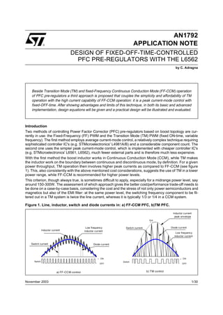
![AN1792 APPLICATION NOTE
2/30
In this area where the TM/CCM usability boundary is uncertain, a third approach that couples the simplicity
and affordability of TM operation with the high current capability of CCM operation can be a solution to the
dilemma.
Generally speaking, FF PWM is not the only alternative when CCM operation is desired. FF PWM modu-
lates both switch ON and OFF times (their sum is constant by definition), and a given converter will operate
in either CCM or DCM depending on the input voltage and the loading conditions. Exactly the same result
can be achieved if the ON-time only is modulated and the OFF-time is kept constant, in which case, how-
ever, the switching frequency will not be fixed anymore (see figure 2). This is referred to as "Fixed-OFF-
Time" (FOT) control. Peak-current-mode control can still be used.
Figure 2. Basic waveforms for Fixed-frequency PWM (a) and Fixed-OFF-Time PWM (b)
The concept of FOT control is not new [1], [2] but, to the author's knowledge, it has never been applied to
PFC pre-regulators to allow CCM operation. In addition to the many advantages and the few drawbacks
that this control technique brings to PFC pre-regulators and that will be highlighted in the following sec-
tions, an important point is that FOT control does not need a specialized control IC. A simple modification
of a standard TM PFC controller operation, requiring just few additional passive parts and no significant
extra cost, is all that is needed.
Operation of a FOT-controlled PFC pre-regulator and its practical implementation
Figure 3 shows a block diagram of a FOT-controlled PFC pre-regulator. An error amplifier (VA) compares
a portion of the pre-regulator's output voltage Vout with a reference VREF and generates an error signal
VC proportional to their difference. VC, a DC voltage by hypothesis, is fed into an input of the multiplier
block and there multiplied by a portion of the rectified input voltage VMULT. At the output of the multiplier,
there will be a rectified sinusoid, VCSREF, whose amplitude is proportional to that of VMULT and to VC,
which represents the sinusoidal reference for PWM modulation. VCSREF is fed into the inverting input of a
comparator that, on the non-inverting input, receives the voltage VCS on the sense resistor Rsense, pro-
portional to the current flowing through the switch M (typically a MOSFET) and the inductor L during the
ON-time of M. When the two voltages are equal, the comparator resets the PWM latch and M, supposed
already ON, will be switched off.
a) Fixed Frequency
Gate
drive
signal
TON
TON'
TON
TON'
TON
TON'
TOFF
TOFF'
TOFF
TOFF'
TSW TSW
a) Fixed OFF-TIme
Gate
drive
signal
TON TON TON
TOFF TOFF
TSW TSW
TSW' TSW'
TON' TON' TON'
TOFF TOFF](data:image/gif;base64,R0lGODlhAQABAIAAAAAAAP///yH5BAEAAAAALAAAAAABAAEAAAIBRAA7)