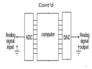
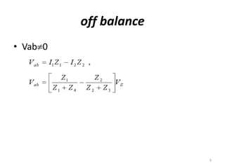
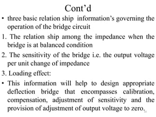
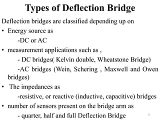
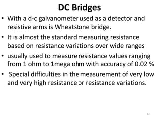
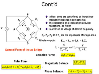
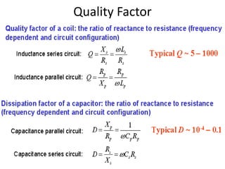
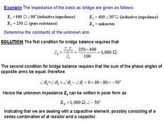
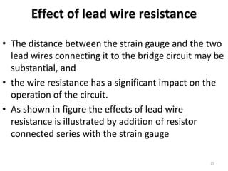
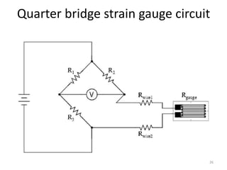
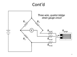
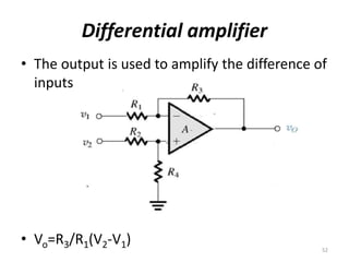
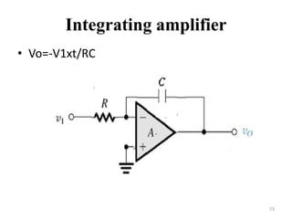
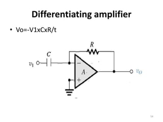
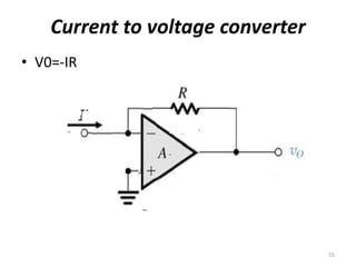
This document discusses sensor signal conditioning, focusing on deflection bridges and their applications in measuring electrical quantities. It explains the operation of different types of deflection bridges, including AC and DC bridges, as well as emphasizing the use of operational amplifiers and instrumentation amplifiers in signal processing. Additionally, it covers aspects of interfacing circuits, including ADC and DAC, for effective interfacing between analog and digital systems.

![Inverting amplifier
• The out put is an inverted (opposite polarity)
form of the input voltage
Vo=-V1[R2/R1]
48](https://image.slidesharecdn.com/chapter31-240508071820-acc7cf6b/85/Chapter-3-signal-conditioning-and-instrumentation-circuit-48-320.jpg)
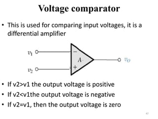
![Non inverting amplifier
• The out put is the non inverted form of the
input
Vo=V1[1+R2/R1]
49](https://image.slidesharecdn.com/chapter31-240508071820-acc7cf6b/85/Chapter-3-signal-conditioning-and-instrumentation-circuit-49-320.jpg)
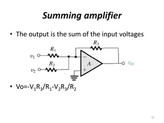
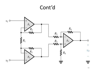
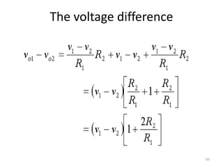
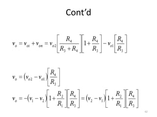
![Cont’d
• The front end of the instrumentation amplifier is a
difference amplifier that can be analyzed by
superposition theorem i.e. the output is due to an
inverting amplifier and non-inverting amplifier.
• The inverting amplifier produces
Voi=-Vo1(R4/R3)
• The non-inverting amplifier produces
Von=Vo2[R4/(R3+R4)][1+R4/R3]
• The output is the sum of the outputs produced by
each input.
61](https://image.slidesharecdn.com/chapter31-240508071820-acc7cf6b/85/Chapter-3-signal-conditioning-and-instrumentation-circuit-61-320.jpg)