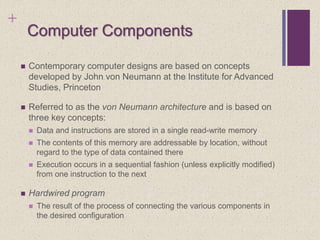
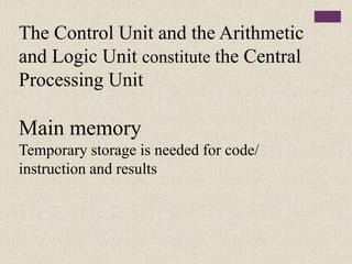
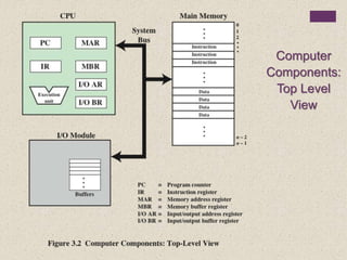
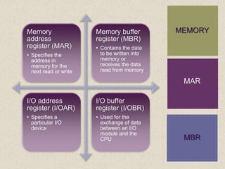
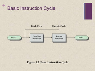
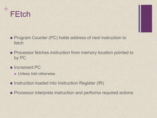
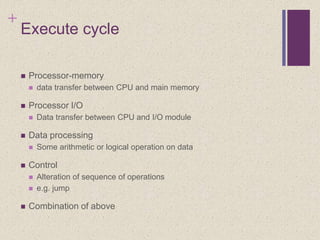
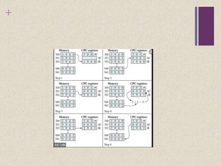
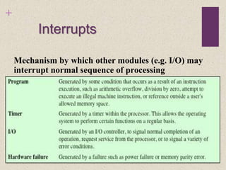
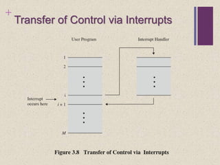
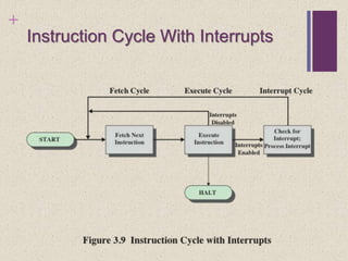
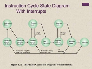
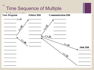
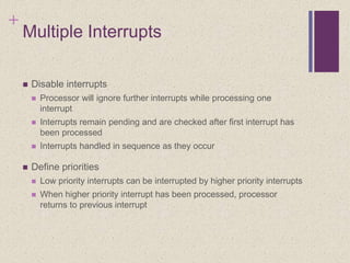
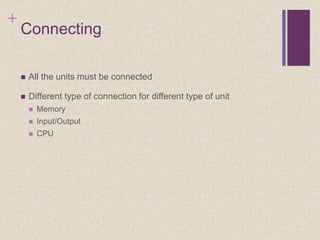
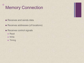
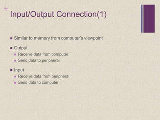
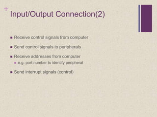
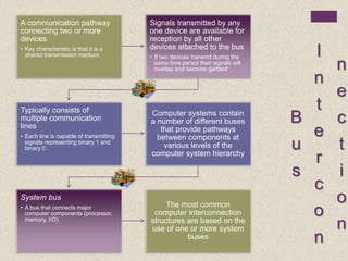
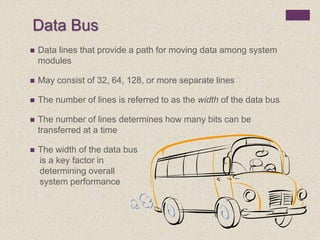
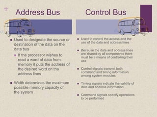
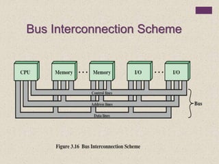
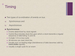
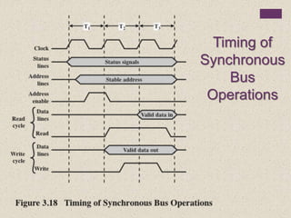
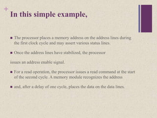
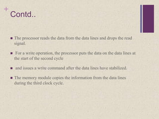
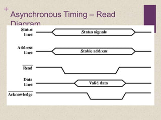
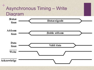
The document discusses the von Neumann architecture and basic components of a computer system. It describes how the CPU, memory, and I/O devices are interconnected via buses. The key buses are the data bus, address bus, and control bus. It explains synchronous and asynchronous timing of bus operations, with synchronous relying on a shared clock and asynchronous using handshaking signals between devices. Interrupts allow I/O devices to signal the CPU to pause normal instruction execution.
3. +
Computer Components
Contemporary computer designs are based on concepts
developed by John von Neumann at the Institute for Advanced
Studies, Princeton
Referred to as the von Neumann architecture and is based on
three key concepts:
Data and instructions are stored in a single read-write memory
The contents of this memory are addressable by location, without
regard to the type of data contained there
Execution occurs in a sequential fashion (unless explicitly modified)
from one instruction to the next
Hardwired program
The result of the process of connecting the various components in
the desired configuration
4. +
Hardwired Program Concept
Hardwired systems are inflexible
General purpose hardware can do different tasks, given correct
control signals
Instead of re-wiring, supply a new set of control signals
6. +
I/O
Components
Software
• A sequence of codes or instructions
• Part of the hardware interprets each instruction
and generates control signals
• Provide a new sequence of codes for each new
program instead of rewiring the hardware
Major components:
• CPU
• Instruction interpreter
• Module of general-purpose arithmetic and logic
functions (ALU & CU)
• I/O Components
• Input module
• Contains basic components for accepting
data and instructions and converting them
into an internal form of signals usable by the
system
• Output module
• Means of reporting results
Software
7. The Control Unit and the Arithmetic
and Logic Unit constitute the Central
Processing Unit
Main memory
Temporary storage is needed for code/
instruction and results
8. Action Categories
• The processor
may perform
some arithmetic
or logic operation
on data
• An instruction
may specify that
the sequence of
execution be
altered
• Data transferred
to or from a
peripheral device
by transferring
between the
processor and an
I/O module
• Data transferred
from processor to
memory or from
memory to
processor
Processor-
memory
Processor-
I/O
Data
processing
Control
10. +
MEMORYMemory
address
register (MAR)
• Specifies the
address in
memory for the
next read or write
Memory buffer
register (MBR)
• Contains the data
to be written into
memory or
receives the data
read from memory
I/O address
register (I/OAR)
• Specifies a
particular I/O
device
I/O buffer
register (I/OBR)
• Used for the
exchange of data
between an I/O
module and the
CPU
MAR
MBR
12. +
Instruction Cycle
At the beginning of each instruction cycle the processor
fetches an instruction from memory
The program counter (PC) holds the address of the instruction
to be fetched next
The processor increments the PC after each instruction fetch
so that it will fetch the next instruction in sequence
The fetched instruction is loaded into the instruction register
(IR)
The processor interprets the instruction and performs the
required action
14. +
FEtch
Program Counter (PC) holds address of next instruction to
fetch
Processor fetches instruction from memory location pointed to
by PC
Increment PC
Unless told otherwise
Instruction loaded into Instruction Register (IR)
Processor interprets instruction and performs required actions
15. +
Execute cycle
Processor-memory
data transfer between CPU and main memory
Processor I/O
Data transfer between CPU and I/O module
Data processing
Some arithmetic or logical operation on data
Control
Alteration of sequence of operations
e.g. jump
Combination of above
21. +
Interrupt Cycle
Added to instruction cycle
Processor checks for interrupt
Indicated by an interrupt signal
If no interrupt, fetch next instruction
If interrupt pending:
Suspend execution of current program
Save context
Set PC to start address of interrupt handler routine
Process interrupt through Interrupt handler routine by generating ISR
(Interrupt Service Request)
Restore context and continue interrupted program
23. +
Multiple Interrupts
Disable interrupts
Processor will ignore further interrupts while processing one
interrupt
Interrupts remain pending and are checked after first interrupt has
been processed
Interrupts handled in sequence as they occur
Define priorities
Low priority interrupts can be interrupted by higher priority interrupts
When higher priority interrupt has been processed, processor
returns to previous interrupt
24. +
Connecting
All the units must be connected
Different type of connection for different type of unit
Memory
Input/Output
CPU
25. +
Memory Connection
Receives and sends data
Receives addresses (of locations)
Receives control signals
Read
Write
Timing
26. +
Input/Output Connection(1)
Similar to memory from computer’s viewpoint
Output
Receive data from computer
Send data to peripheral
Input
Receive data from peripheral
Send data to computer
27. +
Input/Output Connection(2)
Receive control signals from computer
Send control signals to peripherals
Receive addresses from computer
e.g. port number to identify peripheral
Send interrupt signals (control)
28. +
CPU Connection
Reads instruction and data
Writes out data (after processing)
Sends control signals to other units
Receives (& acts on) interrupts
29. B
u
s
I
n
t
e
r
c
o
n
n
e
c
t
i
o
n
A communication pathway
connecting two or more
devices
• Key characteristic is that it is a
shared transmission medium
Signals transmitted by any
one device are available for
reception by all other
devices attached to the bus
• If two devices transmit during the
same time period their signals will
overlap and become garbled
Typically consists of
multiple communication
lines
• Each line is capable of transmitting
signals representing binary 1 and
binary 0
Computer systems contain
a number of different buses
that provide pathways
between components at
various levels of the
computer system hierarchy
System bus
• A bus that connects major
computer components (processor,
memory, I/O)
The most common
computer interconnection
structures are based on the
use of one or more system
buses
30. Data Bus
Data lines that provide a path for moving data among system
modules
May consist of 32, 64, 128, or more separate lines
The number of lines is referred to as the width of the data bus
The number of lines determines how many bits can be
transferred at a time
The width of the data bus
is a key factor in
determining overall
system performance
31. + Address Bus Control Bus
Used to designate the source or
destination of the data on the
data bus
If the processor wishes to
read a word of data from
memory it puts the address of
the desired word on the
address lines
Width determines the maximum
possible memory capacity of
the system
Used to control the access and the
use of the data and address lines
Because the data and address lines
are shared by all components there
must be a means of controlling their
use
Control signals transmit both
command and timing information
among system modules
Timing signals indicate the validity of
data and address information
Command signals specify operations
to be performed
33. +
Timing
Two types of co-ordination of events on bus
a) Synchronous and
b) Asynchronous
Synchronous
Events determined by clock signals
Control Bus includes clock line upon which a clock transmits a regular
sequence of alternating 1s and 0s
A single 1-0 is a bus cycle
All devices can read clock line
Usually sync on leading edge (transference of data becomes valid by
hand shake signals)
Usually a single cycle for an event
35. +
In this simple example,
The processor places a memory address on the address lines during
the first clock cycle and may assert various status lines.
Once the address lines have stabilized, the processor
issues an address enable signal.
For a read operation, the processor issues a read command at the start
of the second cycle. A memory module recognizes the address
and, after a delay of one cycle, places the data on the data lines.
36. +
Contd..
The processor reads the data from the data lines and drops the read
signal.
For a write operation, the processor puts the data on the data lines at
the start of the second cycle
and issues a write command after the data lines have stabilized.
The memory module copies the information from the data lines
during the third clock cycle.
39. +
In this read example of asynchronous
Read diagram
The processor places address and status signals on the bus.
After pausing for these signals to stabilize, it issues a read command,
indicating the presence of valid address and control signals.
The appropriate memory decodes the address and responds by placing
the data on the data line.
Once the data lines have stabilized, the memory module asserts the
acknowledged line to signal the processor that the data are available.
40. +
Once the processor has read the data from the data lines, it de-asserts
the read signal. This causes the memory module to drop the data and
acknowledge lines.
Finally, once the acknowledge line is dropped, the processor removes
the address information.
42. +
A Simple Asynchronous Write
Operation
The processor places the data on the data line at the same time that it
puts signals on the status and address lines.
The memory module responds to the write command by copying the
data from the data lines and then asserting the acknowledge line.
The processor then drops the write signal and the memory module
drops the acknowledge signal.
43. +
Comparison b/w Synchronous and
Asynchronous timing
Synchronous timing is simpler to implement and test. However, it is less
flexible than asynchronous timing.
Because all devices on a synchronous bus are tied to a fixed clock rate,
the system cannot deviate in clock serving time.
With asynchronous timing, a mixture of slow and fast devices, using
older and newer technology, can share a bus.
Synchronous connection every device is going to be served whether it
had something to send or not.