#1 Lecture slides prepared for “Computer Organization and Architecture”, 10/e, by William Stallings, Chapter 3 “A Top Level View of Computer Function and Interconnection”.
#2 At a top level, a computer consists of CPU (central processing unit), memory, and
I/O components, with one or more modules of each type. These components are
interconnected in some fashion to achieve the basic function of the computer, which
is to execute programs. Thus, at a top level, we can characterize a computer system
by describing (1) the external behavior of each component, that is, the data and
control signals that it exchanges with other components and (2) the interconnection
structure and the controls required to manage the use of the interconnection
structure.
This top-level view of structure and function is important because of its
explanatory power in understanding the nature of a computer. Equally important is
its use to understand the increasingly complex issues of performance evaluation. A
grasp of the top-level structure and function offers insight into system bottlenecks,
alternate pathways, the magnitude of system failures if a component fails, and the
ease of adding performance enhancements. In many cases, requirements for greater
system power and fail-safe capabilities are being met by changing the design rather
than merely increasing the speed and reliability of individual components.
This chapter focuses on the basic structures used for computer component
interconnection. As background, the chapter begins with a brief examination of the
basic components and their interface requirements. Then a functional overview is
provided. We are then prepared to examine the use of buses to interconnect system
components.
#3 As discussed in Chapter 2, virtually all contemporary computer designs are based
on concepts developed by John von Neumann at the Institute for Advanced Studies,
Princeton. Such a design is referred to as the von Neumann architecture and is based
on three key concepts:
• Data and instructions are stored in a single read–write memory.
• The contents of this memory are addressable by location, without regard to
the type of data contained there.
• Execution occurs in a sequential fashion (unless explicitly modified) from one
instruction to the next.
The reasoning behind these concepts was discussed in Chapter 2 but is worth
summarizing here. There is a small set of basic logic components that can be
combined in various ways to store binary data and perform arithmetic and logical
operations on that data. If there is a particular computation to be performed, a
configuration of logic components designed specifically for that computation could
be constructed. We can think of the process of connecting the various components
in the desired configuration as a form of programming. The resulting “program” is
in the form of hardware and is termed a hardwired program.
#4 Now consider this alternative. Suppose we construct a general-purpose
configuration of arithmetic and logic functions. This set of hardware will perform
various functions on data depending on control signals applied to the hardware.
In the original case of customized hardware, the system accepts data and produces
results (Figure 3.1a). With general-purpose hardware, the system accepts data and
control signals and produces results. Thus, instead of rewiring the hardware for each
new program, the programmer merely needs to supply a new set of control signals.
How shall control signals be supplied? The answer is simple but subtle. The
entire program is actually a sequence of steps. At each step, some arithmetic or
logical operation is performed on some data. For each step, a new set of control
signals is needed. Let us provide a unique code for each possible set of control
signals, and let us add to the general-purpose hardware a segment that can accept a
code and generate control signals (Figure 3.1b).
#5 Programming is now much easier. Instead of rewiring the hardware for each
new program, all we need to do is provide a new sequence of codes. Each code
is, in effect, an instruction, and part of the hardware interprets each instruction
and generates control signals. To distinguish this new method of programming, a
sequence of codes or instructions is called software.
Figure 3.1b indicates two major components of the system: an instruction
interpreter and a module of general-purpose arithmetic and logic functions. These
two constitute the CPU. Several other components are needed to yield a functioning
computer. Data and instructions must be put into the system. For this we need some
sort of input module. This module contains basic components for accepting data
and instructions in some form and converting them into an internal form of signals
usable by the system. A means of reporting results is needed, and this is in the form
of an output module. Taken together, these are referred to as I/O components.
#6 One more component is needed. An input device will bring instructions and
data in sequentially. But a program is not invariably executed sequentially; it may
jump around (e.g., the IAS jump instruction). Similarly, operations on data may
require access to more than just one element at a time in a predetermined sequence.
Thus, there must be a place to store temporarily both instructions and data. That
module is called memory, or main memory, to distinguish it from external storage or
peripheral devices. Von Neumann pointed out that the same memory could be used
to store both instructions and data.
The CPU exchanges data with memory. For this purpose, it typically
makes use of two internal (to the CPU) registers: a memory address register (MAR),
which specifies the address in memory for the next read or write, and a memory
buffer register (MBR), which contains the data to be written into memory or receives
the data read from memory. Similarly, an I/O address register (I/OAR) specifies a
particular I/O device. An I/O buffer (I/OBR) register is used for the exchange of
data between an I/O module and the CPU.
#7 Figure 3.2 illustrates these top-level components and suggests the interactions
among them.
A memory module consists of a set of locations, defined by sequentially
numbered addresses. Each location contains a binary number that can be interpreted
as either an instruction or data. An I/O module transfers data from external devices
to CPU and memory, and vice versa. It contains internal buffers for temporarily
holding these data until they can be sent on.
#8 The basic function performed by a computer is execution of a program, which consists
of a set of instructions stored in memory. The processor does the actual work by
executing instructions specified in the program. This section provides an overview of
the key elements of program execution. In its simplest form, instruction processing
consists of two steps: The processor reads (fetches ) instructions from memory one
at a time and executes each instruction. Program execution consists of repeating
the process of instruction fetch and instruction execution. The instruction execution
may involve several operations and depends on the nature of the instruction (see, for
example, the lower portion of Figure 2.4).
The processing required for a single instruction is called an instruction cycle.
Using the simplified two-step description given previously, the instruction cycle is
depicted in Figure 3.3. The two steps are referred to as the fetch cycle and the execute
cycle. Program execution halts only if the machine is turned off, some sort of unrecoverable
error occurs, or a program instruction that halts the computer is encountered.
#9 At the beginning of each instruction cycle, the processor fetches an instruction
from memory. In a typical processor, a register called the program counter (PC)
holds the address of the instruction to be fetched next. Unless told otherwise, the
processor always increments the PC after each instruction fetch so that it will fetch
the next instruction in sequence (i.e., the instruction located at the next higher memory
address). So, for example, consider a computer in which each instruction occupies
one 16-bit word of memory. Assume that the program counter is set to memory
location 300, where the location address refers to a 16-bit word. The processor will
next fetch the instruction at location 300. On succeeding instruction cycles, it will
fetch instructions from locations 301, 302, 303, and so on. This sequence may be
altered, as explained presently.
The fetched instruction is loaded into a register in the processor known as
the instruction register (IR). The instruction contains bits that specify the action
the processor is to take. The processor interprets the instruction and performs the
required action.
#10 In general, these actions fall into four categories:
Processor-memory: Data may be transferred from processor to memory or
from memory to processor.
• Processor-I/O: Data may be transferred to or from a peripheral device by
transferring between the processor and an I/O module.
• Data processing: The processor may perform some arithmetic or logic operation
on data.
• Control: An instruction may specify that the sequence of execution be altered.
For example, the processor may fetch an instruction from location 149, which
specifies that the next instruction be from location 182. The processor will
remember this fact by setting the program counter to 182. Thus, on the next
fetch cycle, the instruction will be fetched from location 182 rather than 150.
An instruction’s execution may involve a combination of these actions.
#11 Consider a simple example using a hypothetical machine that includes the
characteristics listed in Figure 3.4. The processor contains a single data register,
called an accumulator (AC). Both instructions and data are 16 bits long. Thus, it is
convenient to organize memory using 16-bit words. The instruction format provides
4 bits for the opcode, so that there can be as many as 24 = 16 different opcodes, and
up to 212 = 4096 (4K) words of memory can be directly addressed.
#12 Figure 3.5 illustrates a partial program execution, showing the relevant
portions of memory and processor registers. The program fragment shown adds
the contents of the memory word at address 940 to the contents of the memory
word at address 941 and stores the result in the latter location. Three instructions,
which can be described as three fetch and three execute cycles, are required:
1. The PC contains 300, the address of the first instruction. This instruction (the
value 1940 in hexadecimal) is loaded into the instruction register IR, and
the PC is incremented. Note that this process involves the use of a memory
address register and a memory buffer register. For simplicity, these intermediate
registers are ignored.
2. The first 4 bits (first hexadecimal digit) in the IR indicate that the AC is to be
loaded. The remaining 12 bits (three hexadecimal digits) specify the address
(940) from which data are to be loaded.
3. The next instruction (5941) is fetched from location 301, and the PC is
incremented.
4. The old contents of the AC and the contents of location 941 are added, and
the result is stored in the AC.
5. The next instruction (2941) is fetched from location 302, and the PC is
incremented.
6. The contents of the AC are stored in location 941.
In this example, three instruction cycles, each consisting of a fetch cycle and an
execute cycle, are needed to add the contents of location 940 to the contents of 941.
With a more complex set of instructions, fewer cycles would be needed. Some older
processors, for example, included instructions that contain more than one memory
address. Thus, the execution cycle for a particular instruction on such processors could
involve more than one reference to memory. Also, instead of memory references, an
instruction may specify an I/O operation.
#13 The execution cycle for a particular instruction may involve more than one
reference to memory. Also, instead of memory references, an instruction may specify
an I/O operation. With these additional considerations in mind, Figure 3.6 provides
a more detailed look at the basic instruction cycle of Figure 3.3. The figure is in the
form of a state diagram.
For any given instruction cycle, some states may be null and
others may be visited more than once. The states can be described as follows:
• Instruction address calculation (iac): Determine the address of the next
instruction to be executed. Usually, this involves adding a fixed number to
the address of the previous instruction. For example, if each instruction is 16
bits long and memory is organized into 16-bit words, then add 1 to the previous
address. If, instead, memory is organized as individually addressable 8-bit
bytes, then add 2 to the previous address.
• Instruction fetch (if): Read instruction from its memory location into the
processor.
• Instruction operation decoding (iod): Analyze instruction to determine type
of operation to be performed and operand(s) to be used.
• Operand address calculation (oac): If the operation involves reference to an
operand in memory or available via I/O, then determine the address of the
operand.
• Operand fetch (of): Fetch the operand from memory or read it in from I/O.
• Data operation (do): Perform the operation indicated in the instruction.
• Operand store (os): Write the result into memory or out to I/O.
States in the upper part of Figure 3.6 involve an exchange between the
processor and either memory or an I/O module. States in the lower part of the
diagram involve only internal processor operations. The oac state appears twice,
because an instruction may involve a read, a write, or both. However, the action performed
during that state is fundamentally the same in both cases, and so only a single
state identifier is needed.
Also note that the diagram allows for multiple operands and multiple results,
because some instructions on some machines require this. For example, the PDP-11
instruction ADD A,B results in the following sequence of states: iac, if, iod, oac, of,
oac, of, do, oac, os.
Finally, on some machines, a single instruction can specify an operation to be performed
on a vector (one-dimensional array) of numbers or a string (one-dimensional
array) of characters. As Figure 3.6 indicates, this would involve repetitive operand fetch
and/or store operations.
#14 Virtually all computers provide a mechanism by which other modules (I/O, memory)
may interrupt the normal processing of the processor. Table 3.1 lists the most common
classes of interrupts. The specific nature of these interrupts is examined
later in this book, especially in Chapters 7 and 14. However, we need to introduce the concept
now to understand more clearly the nature of the instruction cycle and the implications
of interrupts on the interconnection structure.
#15 Interrupts are provided primarily as a way to improve processing efficiency.
For example, most external devices are much slower than the processor. Suppose
that the processor is transferring data to a printer using the instruction cycle scheme
of Figure 3.3. After each write operation, the processor must pause and remain
idle until the printer catches up. The length of this pause may be on the order of
many hundreds or even thousands of instruction cycles that do not involve memory.
Clearly, this is a very wasteful use of the processor.
Figure 3.7a illustrates this state of affairs. The user program performs a series
of WRITE calls interleaved with processing. Code segments 1, 2, and 3 refer to
sequences of instructions that do not involve I/O. The WRITE calls are to an I/O
program that is a system utility and that will perform the actual I/O operation. The
I/O program consists of three sections:
• A sequence of instructions, labeled 4 in the figure, to prepare for the actual
I/O operation. This may include copying the data to be output into a special
buffer and preparing the parameters for a device command.
• The actual I/O command. Without the use of interrupts, once this command is
issued, the program must wait for the I/O device to perform the requested function
(or periodically poll the device). The program might wait by simply repeatedly
performing a test operation to determine if the I/O operation is done.
• A sequence of instructions, labeled 5 in the figure, to complete the operation.
This may include setting a flag indicating the success or failure of the operation.
Because the I/O operation may take a relatively long time to complete, the I/O
program is hung up waiting for the operation to complete; hence, the user program
is stopped at the point of the WRITE call for some considerable period of time.
With interrupts, the processor can
be engaged in executing other instructions while an I/O operation is in progress.
Consider the flow of control in Figure 3.7b. As before, the user program reaches a
point at which it makes a system call in the form of a WRITE call. The I/O program
that is invoked in this case consists only of the preparation code and the actual I/O
command. After these few instructions have been executed, control returns to the
user program. Meanwhile, the external device is busy accepting data from computer
memory and printing it. This I/O operation is conducted concurrently with the
execution of instructions in the user program.
When the external device becomes ready to be serviced—that is, when it is
ready to accept more data from the processor—the I/O module for that external
device sends an interrupt request signal to the processor. The processor responds by
suspending operation of the current program, branching off to a program to service
that particular I/O device, known as an interrupt handler, and resuming the original
execution after the device is serviced. The points at which such interrupts occur are
indicated by an asterisk in Figure 3.7b.
Let us try to clarify what is happening in Figure 3.7. We have a user program
that contains two WRITE commands. There is a segment of code at the beginning,
then one WRITE command, then a second segment of code, then a second WRITE
command, then a third and final segment of code. The WRITE command invokes the
I/O program provided by the OS. Similarly, the I/O program consists of a segment
of code, followed by an I/O command, followed by another segment of code. The I/O
command invokes a hardware I/O operation.
#16 From the point of view of the user program, an interrupt is just that: an interruption
of the normal sequence of execution. When the interrupt processing is completed,
execution resumes (Figure 3.8). Thus, the user program does not have to contain any
special code to accommodate interrupts; the processor and the operating system are
responsible for suspending the user program and then resuming it at the same point.
#17 To accommodate interrupts, an interrupt cycle is added to the instruction
cycle, as shown in Figure 3.9. In the interrupt cycle, the processor checks to see if
any interrupts have occurred, indicated by the presence of an interrupt signal. If no
interrupts are pending, the processor proceeds to the fetch cycle and fetches the
next instruction of the current program. If an interrupt is pending, the processor
does the following:
• It suspends execution of the current program being executed and saves its
context. This means saving the address of the next instruction to be executed
(current contents of the program counter) and any other data relevant to the
processor’s current activity.
• It sets the program counter to the starting address of an interrupt handler routine.
The processor now proceeds to the fetch cycle and fetches the first instruction
in the interrupt handler program, which will service the interrupt. The interrupt
handler program is generally part of the operating system. Typically, this program
determines the nature of the interrupt and performs whatever actions are needed.
In the example we have been using, the handler determines which I/O module
generated the interrupt and may branch to a program that will write more data out
to that I/O module. When the interrupt handler routine is completed, the processor
can resume execution of the user program at the point of interruption.
It is clear that there is some overhead involved in this process. Extra instructions
must be executed (in the interrupt handler) to determine the nature of the interrupt
and to decide on the appropriate action. Nevertheless, because of the relatively large
amount of time that would be wasted by simply waiting on an I/O operation, the
processor can be employed much more efficiently with the use of interrupts.
#18 To appreciate the gain in efficiency, consider Figure 3.10, which is a timing diagram
based on the flow of control in Figures 3.7a and 3.7b. In this figure, user program
code segments are shaded green, and I/O program code segments are shaded
gray. Figure 3.10a shows the case in which interrupts are not used. The processor must
wait while an I/O operation is performed.
Figures 3.7b and 3.10b assume that the time required for the I/O operation is
relatively short: less than the time to complete the execution of instructions between write
operations in the user program. In this case, the segment of code labeled code segment
2 is interrupted. A portion of the code (2a) executes (while the I/O operation is performed)
and then the interrupt occurs (upon the completion of the I/O operation). After
the interrupt is serviced, execution resumes with the remainder of code segment 2 (2b).
#19 The more typical case, especially for a slow device such as a printer, is that the
I/O operation will take much more time than executing a sequence of user instructions.
Figure 3.7c indicates this state of affairs. In this case, the user program reaches
the second WRITE call before the I/O operation spawned by the first call is complete.
The result is that the user program is hung up at that point. When the preceding
I/O operation is completed, this new WRITE call may be processed, and a new
I/O operation may be started. Figure 3.11 shows the timing for this situation with
and without the use of interrupts. We can see that there is still a gain in efficiency
because part of the time during which the I/O operation is under way overlaps with
the execution of user instructions.
#20 Figure 3.12 shows a revised instruction cycle state diagram that includes
interrupt cycle processing.
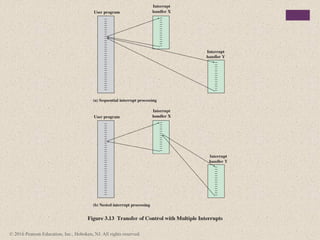
#21 Two approaches can be taken to dealing with multiple interrupts. The first is to
disable interrupts while an interrupt is being processed. A disabled interrupt simply
means that the processor can and will ignore that interrupt request signal. If an interrupt
occurs during this time, it generally remains pending and will be checked by
the processor after the processor has enabled interrupts. Thus, when a user program
is executing and an interrupt occurs, interrupts are disabled immediately. After the
interrupt handler routine completes, interrupts are enabled before resuming the
user program, and the processor checks to see if additional interrupts have occurred.
This approach is nice and simple, as interrupts are handled in strict sequential order
(Figure 3.13a).
The drawback to the preceding approach is that it does not take into account
relative priority or time-critical needs. For example, when input arrives from the
communications line, it may need to be absorbed rapidly to make room for more
input. If the first batch of input has not been processed before the second batch
arrives, data may be lost.
A second approach is to define priorities for interrupts and to allow an
interrupt of higher priority to cause a lower-priority interrupt handler to be itself
interrupted (Figure 3.13b).
#22 As an example of this second approach, consider a
system with three I/O devices: a printer, a disk, and a communications line, with
increasing priorities of 2, 4, and 5, respectively. Figure 3.14 illustrates a possible
sequence. A user program begins at t = 0. At t = 10, a printer interrupt occurs; user
information is placed on the system stack and execution continues at the printer
interrupt service routine (ISR). While this routine is still executing, at t = 15, a
communications interrupt occurs. Because the communications line has higher
priority than the printer, the interrupt is honored. The printer ISR is interrupted,
its state is pushed onto the stack, and execution
continues at the communications ISR. While this routine is executing, a disk interrupt
occurs (t = 20). Because this interrupt is of lower priority, it is simply held, and the communications ISR runs
to completion.
When the communications ISR is complete (t = 25), the previous processor
state is restored, which is the execution of the printer ISR. However, before even a
single instruction in that routine can be executed, the processor honors the higher priority
disk interrupt and control transfers to the disk ISR. Only when that routine
is complete
(t = 35) is the printer ISR resumed. When that routine completes (t = 40),
control finally returns to the user program.
#23 An I/O module (e.g., a disk controller) can exchange data directly with the
processor. Just as the processor can initiate a read or write with memory, designating
the address of a specific location, the processor can also read data from or write data
to an I/O module. In this latter case, the processor identifies a specific device that is
controlled by a particular I/O module. Thus, an instruction sequence similar in form to
that of Figure 3.5 could occur, with I/O instructions rather than memory-referencing
instructions.
In some cases, it is desirable to allow I/O exchanges to occur directly with
memory. In such a case, the processor grants to an I/O module the authority to read
from or write to memory, so that the I/O-memory transfer can occur without tying up
the processor. During such a transfer, the I/O module issues read or write commands
to memory, relieving the processor of responsibility for the exchange. This operation
is known as direct memory access (DMA) and is examined in Chapter 7.
#24 A computer consists of a set of components or modules of three basic types
(processor, memory, I/O) that communicate with each other. In effect, a computer is
a network of basic modules. Thus, there must be paths for connecting the modules.
The collection of paths connecting the various modules is called the interconnection
structure. The design of this structure will depend on the exchanges that
must be made among modules.
Figure 3.15 suggests the types of exchanges that are needed by indicating the
major forms of input and output for each module type:
• Memory: Typically, a memory module will consist of N words of equal length.
Each word is assigned a unique numerical address (0, 1, …, N - 1). A word of
data can be read from or written into the memory. The nature of the operation
is indicated by read and write control signals. The location for the operation is
specified by an address.
• I/O module: From an internal (to the computer system) point of view, I/O
is functionally similar to memory. There are two operations, read and write.
Further, an I/O module may control more than one external device. We can
refer to each of the interfaces to an external device as a port and give each
a unique address (e.g., 0, 1, …, M - 1). In addition, there are external data
paths for the input and output of data with an external device. Finally, an I/O
module may be able to send interrupt signals to the processor.
• Processor: The processor reads in instructions and data, writes out data after
processing, and uses control signals to control the overall operation of the
system. It also receives interrupt signals.
#25 The preceding list defines the data to be exchanged. The interconnection
structure must support the following types of transfers:
• Memory to processor: The processor reads an instruction or a unit of data
from memory.
• Processor to memory: The processor writes a unit of data to memory.
• I/O to processor: The processor reads data from an I/O device via an I/O
module.
• Processor to I/O: The processor sends data to the I/O device.
• I/O to or from memory: For these two cases, an I/O module is allowed to exchange
data directly with memory, without going through the processor, using
direct memory access.
Over the years, a number of interconnection structures have been tried. By
far the most common are (1) the bus and various multiple-bus structures, and (2)
point-to-point interconnection structures with packetized data transfer. We devote
the remainder of this chapter for a discussion of these structures.
#26 The bus was the dominant means of computer system component interconnection
for decades. For general-purpose computers, it has gradually given way to various
point-to-point interconnection structures, which now dominate computer system
design. However, bus structures are still commonly used for embedded systems, particularly
microcontrollers. In this section, we give a brief overview of bus structure.
Appendix C provides more detail.
A bus is a communication pathway connecting two or more devices. A key characteristic
of a bus is that it is a shared transmission medium. Multiple devices connect
to the bus, and a signal transmitted by any one device is available for reception by
all other devices attached to the bus. If two devices transmit during the same time
period, their signals will overlap and become garbled. Thus, only one device at a
time can successfully transmit.
Typically, a bus consists of multiple communication pathways, or lines. Each
line is capable of transmitting signals representing binary 1 and binary 0. Over time,
a sequence of binary digits can be transmitted across a single line. Taken together,
several lines of a bus can be used to transmit binary digits simultaneously (in parallel).
For example, an 8-bit unit of data can be transmitted over eight bus lines.
Computer systems contain a number of different buses that provide pathways
between components at various levels of the computer system hierarchy. A bus that
connects major computer components (processor, memory, I/O) is called a system
bus. The most common computer interconnection structures are based on the use of
one or more system buses.
#27 A system bus consists, typically, of from about fifty to hundreds of separate lines.
The data lines provide a path for moving data among system modules. These
lines, collectively, are called the data bus. The data bus may consist of 32, 64, 128, or
even more separate lines, the number of lines being referred to as the width of the
data bus. Because each line can carry only 1 bit at a time, the number of lines determines
how many bits can be transferred at a time. The width of the data bus is a key
factor in determining overall system performance. For example, if the data bus is
32 bits wide and each instruction is 64 bits long, then the processor must access the
memory module twice during each instruction cycle.
#28 The address lines are used to designate the source or destination of the data on
the data bus. For example, if the processor wishes to read a word (8, 16, or 32 bits)
of data from memory, it puts the address of the desired word on the address lines.
Clearly, the width of the address bus determines the maximum possible memory
capacity of the system. Furthermore, the address lines are generally also used to
address I/O ports. Typically, the higher-order bits are used to select a particular
module on the bus, and the lower-order bits select a memory location or I/O port
within the module. For example, on an 8-bit address bus, address 01111111 and
below might reference locations in a memory module (module 0) with 128 words
of memory, and address 10000000 and above refer to devices attached to an I/O
module (module 1).
The control lines are used to control the access to and the use of the data and
address lines. Because the data and address lines are shared by all components,
there must be a means of controlling their use. Control signals transmit both command
and timing information among system modules. Timing signals indicate the
validity of data and address information. Command signals specify operations to be
performed. Typical control lines include:
• Memory write: causes data on the bus to be written into the addressed location
• Memory read: causes data from the addressed location to be placed on the
bus
• I/O write: causes data on the bus to be output to the addressed I/O port
• I/O read: causes data from the addressed I/O port to be placed on the bus
• Transfer ACK: indicates that data have been accepted from or placed on the
bus
• Bus request: indicates that a module needs to gain control of the bus
• Bus grant: indicates that a requesting module has been granted control of the
bus
• Interrupt request: indicates that an interrupt is pending
• Interrupt ACK: acknowledges that the pending interrupt has been recognized
• Clock: is used to synchronize operations
• Reset: initializes all modules
#29 Each line is assigned a particular meaning or function. Although there are
many different bus designs, on any bus the lines can be classified into three functional
groups (Figure 3.16): data, address, and control lines. In addition, there may
be power distribution lines that supply power to the attached modules.
The operation of the bus is as follows. If one module wishes to send data to
another, it must do two things: (1) obtain the use of the bus, and (2) transfer data
via the bus. If one module wishes to request data from another module, it must (1)
obtain the use of the bus, and (2) transfer a request to the other module over the
appropriate control and address lines. It must then wait for that second module to
send the data.
#30 The shared bus architecture was the standard approach to interconnection between
the processor and other components (memory, I/O, and so on) for decades. But
contemporary systems increasingly rely on point-to-point interconnection rather
than shared buses.
The principal reason driving the change from bus to point-to-point interconnect
was the electrical constraints encountered with increasing the frequency of wide
synchronous buses. At higher and higher data rates, it becomes increasingly difficult
to perform the synchronization and arbitration functions in a timely fashion. Further,
with the advent of multi-core chips, with multiple processors and significant memory
on a single chip, it was found that the use of a conventional shared bus on the same
chip magnified the difficulties of increasing bus data rate and reducing bus latency
to keep up interconnect has lower latency, higher data rate, and better scalability.
#31 In this section, we look at an important and representative example of the
point-to-point interconnect approach: Intel’s QuickPath Interconnect (QPI), which
was introduced in 2008.
The following are significant characteristics of QPI and other point-to-point
interconnect schemes:
• Multiple direct connections: Multiple components within the system enjoy
direct pairwise connections to other components. This eliminates the need for
arbitration found in shared transmission systems.
• Layered protocol architecture: As found in network environments, such as
TCP/IP-based data networks, these processor-level interconnects use a layered
protocol architecture, rather than the simple use of control signals found in
shared bus arrangements.
• Packetized data transfer: Data are not sent as a raw bit stream. Rather, data
are sent as a sequence of packets, each of which includes control headers and
error control codes.
#32 Figure 3.17 illustrates a typical use of QPI on a multi-core computer. The
QPI links (indicated by the green arrow pairs in the figure) form a switching fabric
that enables data to move throughout the network. Direct QPI connections can be
established between each pair of core processors. If core A in Figure 3.20 needs to
access the memory controller in core D, it sends its request through either cores B
or C, which must in turn forward that request on to the memory controller in core D.
Similarly, larger systems with eight or more processors can be built using processors
with three links and routing traffic through intermediate processors.
In addition, QPI is used to connect to an I/O module, called an I/O hub (IOH).
The IOH acts as a switch directing traffic to and from I/O devices. Typically in newer
systems, the link from the IOH to the I/O device controller uses an interconnect
technology called PCI Express (PCIe), described later in this chapter. The IOH translates
between the QPI protocols and formats and the PCIe protocols and formats. A
core also links to a main memory module (typically the memory uses dynamic access
random memory (DRAM) technology) using a dedicated memory bus.
#33 QPI is defined as a four-layer protocol architecture, encompassing the
following layers (Figure 3.18):
• Physical: Consists of the actual wires carrying the signals, as well as circuitry
and logic to support ancillary features required in the transmission and receipt
of the 1s and 0s. The unit of transfer at the Physical layer is 20 bits, which is
called a Phit (physical unit).
Link: Responsible for reliable transmission and flow control. The Link layer’s
unit of transfer is an 80-bit Flit (flow control unit).
• Routing: Provides the framework for directing packets through the fabric.
• Protocol: The high-level set of rules for exchanging packets of data between
devices. A packet is comprised of an integral number of Flits.
#34 Figure 3.19 shows the physical architecture of a QPI port. The QPI port consists of
84 individual links grouped as follows. Each data path consists of a pair of wires that
transmits data one bit at a time; the pair is referred to as a lane. There are 20 data lanes
in each direction (transmit and receive), plus a clock lane in each direction. Thus, QPI
is capable of transmitting 20 bits in parallel in each direction. The 20-bit unit is referred
to as a phit. Typical signaling speeds of the link in current products calls for operation
at 6.4 GT/s (transfers per second). At 20 bits per transfer, that adds up to 16 GB/s, and
since QPI links involve dedicated bidirectional pairs, the total capacity is 32 GB/s.
The lanes in each direction are grouped into four quadrants of 5 lanes each.
In some applications, the link can also operate at half or quarter widths in order to
reduce power consumption or work around failures.
The form of transmission on each lane is known as differential signaling, or
balanced transmission. With balanced transmission, signals are transmitted as a
current that travels down one conductor and returns on the other. The binary value
depends on the voltage difference. Typically, one line has a positive voltage value
and the other line has zero voltage, and one line is associated with binary 1 and one
line is associated with binary 0. Specifically, the technique used by QPI is known as
low-voltage differential signaling (LVDS). In a typical implementation, the transmitter
injects a small current into one wire or the other, depending on the logic level to
be sent. The current passes through a resistor at the receiving end, and then returns
in the opposite direction along the other wire. The receiver senses the polarity of the
voltage across the resistor to determine the logic level.
#35 Another function performed by the physical layer is that it manages the translation
between 80-bit flits and 20-bit phits using a technique known as multilane distribution.
The flits can be considered as a bit stream that is distributed across the data
lanes in a round-robin fashion (first bit to first lane, second bit to second lane, etc.), as
illustrated in Figure 3.20. This approach enables QPI to achieve very high data rates
by implementing the physical link between two ports as multiple parallel channels.
#36 The QPI link layer performs two key functions: flow control and error control. These
functions are performed as part of the QPI link layer protocol, and operate on the
level of the flit (flow control unit). Each flit consists of a 72-bit message payload
and an 8-bit error control code called a cyclic redundancy check (CRC). We discuss error
control codes in Chapter 5.
A flit payload may consist of data or message information. The data flits transfer
the actual bits of data between cores or between a core and an IOH. The message
flits are used for such functions as flow control, error control, and cache coherence.
We discuss cache coherence in Chapters 5 and 17.
The flow control function is needed to ensure that a sending QPI entity does
not overwhelm a receiving QPI entity by sending data faster than the receiver can
process the data and clear buffers for more incoming data. To control the flow of
data, QPI makes use of a credit scheme. During initialization, a sender is given a set
number of credits to send flits to a receiver. Whenever a flit is sent to the receiver,
the sender decrements its credit counters by one credit. Whenever a buffer is freed
at the receiver, a credit is returned to the sender for that buffer. Thus, the receiver
controls that pace at which data is transmitted over a QPI link.
Occasionally, a bit transmitted at the physical layer is changed during transmission,
due to noise or some other phenomenon. The error control function at the
link layer detects and recovers from such bit errors, and so isolates higher layers
from experiencing bit errors. The procedure works as follows for a flow of data
from system A to system B:
1. As mentioned, each 80-bit flit includes an 8-bit CRC field. The CRC is a function
of the value of the remaining 72 bits. On transmission, A calculates a
CRC value for each flit and inserts that value into the flit.
2. When a flit is received, B calculates a CRC value for the 72-bit payload and
compares this value with the value of the incoming CRC value in the flit. If the
two CRC values do not match, an error has been detected.
3. When B detects an error, it sends a request to A to retransmit the flit that is
in error. However, because A may have had sufficient credit to send a stream
of flits, so that additional flits have been transmitted after the flit in error and
before A receives the request to retransmit. Therefore, the request is for A to
back up and retransmit the damaged flit plus all subsequent flits.
#37 The Routing layer is used to determine the course that a packet will traverse across
the available system interconnects. Routing tables are defined by firmware and
describe the possible paths that a packet can follow. In small configurations, such as
a two-socket platform, the routing options are limited and the routing tables quite
simple. For larger systems, the routing table options are more complex, giving the
flexibility of routing and rerouting traffic depending on how (1) devices are populated
in the platform, (2) system resources are partitioned, and (3) reliability events
result in mapping around a failing resource.
QPI Protocol Layer
In this layer, the packet is defined as the unit of transfer. The packet contents
definition is standardized with some flexibility allowed to meet differing market
segment requirements. One key function performed at this level is a cache coherency
protocol, which deals with making sure that main memory values held in
multiple caches are consistent. A typical data packet payload is a block of data
being sent to or from a cache.
#38 The peripheral component interconnect (PCI) is a popular high-bandwidth, processor independent
bus that can function as a mezzanine or peripheral bus. Compared with
other common bus specifications, PCI delivers better system performance for high speed
I/O subsystems (e.g., graphic display adapters, network interface controllers,
and disk controllers).
Intel began work on PCI in 1990 for its Pentium-based systems. Intel soon
released all the patents to the public domain and promoted the creation of an
industry association, the PCI Special Interest Group (SIG), to develop further and
maintain the compatibility of the PCI specifications. The result is that PCI has been
widely adopted and is finding increasing use in personal computer, workstation, and
server systems. Because the specification is in the public domain and is supported
by a broad cross section of the microprocessor and peripheral industry, PCI products
built by different vendors are compatible.
As with the system bus discussed in the preceding sections, the bus-based PCI
scheme has not been able to keep pace with the data rate demands of attached
devices. Accordingly, a new version, known as PCI Express (PCIe) has been developed.
PCIe, as with QPI, is a point-to-point interconnect scheme intended to replace
bus-based schemes such as PCI.
A key requirement for PCIe is high capacity to support the needs of higher data
rate I/O devices, such as Gigabit Ethernet. Another requirement deals with the need
to support time-dependent data streams. Applications such as video-on-demand and
audio redistribution are putting real-time constraints on servers too. Many communications
applications and embedded PC control systems also process data in real-
time.
Today’s platforms must also deal with multiple concurrent transfers at ever-increasing
data rates. It is no longer acceptable to treat all data as equal—it is more important,
for example, to process streaming data first since late real-time data is as useless as no
data. Data needs to be tagged so that an I/O system can prioritize its flow throughout
the platform.
#39 Figure 3.21 shows a typical configuration that supports the use of PCIe. A root
complex device, also referred to as a chipset or a host bridge, connects the processor
and memory subsystem to the PCI Express switch fabric comprising one or
more PCIe and PCIe switch devices. The root complex acts as a buffering device, to
deal with difference in data rates between I/O controllers and memory and processor
components. The root complex also translates between PCIe transaction formats
and the processor and memory signal and control requirements. The chipset
will typically support multiple PCIe ports, some of which attach directly to a PCIe
device and one or more that attach to a switch that manages multiple PCIe streams.
PCIe links from the chipset may attach to the following kinds of devices that implement
PCIe:
• Switch: The switch manages multiple PCIe streams.
• PCIe endpoint: An I/O device or controller that implements PCIe, such as
a Gigabit Ethernet switch, a graphics or video controller, disk interface, or a
communications controller.
• Legacy endpoint: Legacy endpoint category is intended for existing designs
that have been migrated to PCI Express, and it allows legacy behaviors such
as use of I/O space and locked transactions. PCI Express endpoints are not
permitted to require the use of I/O space at runtime and must not use locked
transactions. By distinguishing these categories, it is possible for a system
designer to restrict or eliminate legacy behaviors that have negative impacts
on system performance and robustness.
• PCIe/PCI bridge: Allows older PCI devices to be connected to PCIe-based
systems.
#40 As with QPI, PCIe interactions are defined using a protocol architecture. The
PCIe protocol architecture encompasses the following layers (Figure 3.22):
Physical: Consists of the actual wires carrying the signals, as well as circuitry
and logic to support ancillary features required in the transmission and receipt
of the 1s and 0s.
• Data link: Is responsible for reliable transmission and flow control. Data
packets generated and consumed by the DLL are called Data Link Layer
Packets (DLLPs).
• Transaction: Generates and consumes data packets used to implement load/
store data transfer mechanisms and also manages the flow control of those
packets between the two components on a link. Data packets generated and
consumed by the TL are called Transaction Layer Packets (TLPs).
Above the TL are software layers that generate read and write requests that
are transported by the transaction layer to the I/O devices using a packet-based
transaction protocol.
#41 Similar to QPI, PCIe is a point-to-point architecture. Each PCIe port consists of a
number of bidirectional lanes (note that in QPI, the lane refers to transfer in one
direction only). Transfer in each direction in a lane is by means of differential signaling
over a pair of wires. A PCI port can provide 1, 4, 6, 16, or 32 lanes. In what
follows, we refer to the PCIe 3.0 specification, introduced in late 2010.
As with QPI, PCIe uses a multilane distribution technique. Figure 3.23 shows
an example for a PCIe port consisting of four lanes. Data are distributed to the four
lanes 1 byte at a time using a simple round-robin scheme. At each physical lane,
data are buffered and processed 16 bytes (128 bits) at a time. Each block of 128 bits
is encoded into a unique 130-bit codeword for transmission; this is referred to as
128b/130b encoding. Thus, the effective data rate of an individual lane is reduced
by a factor of 128/130.
To understand the rationale for the 128b/130b encoding, note that unlike
QPI, PCIe does not use its clock line to synchronize the bit stream. That is, the
clock line is not used to determine the start and end point of each incoming bit; it
is used for other signaling purposes only. However, it is necessary for the receiver
to be synchronized with the transmitter, so that the receiver knows when each bit
begins and ends. If there is any drift between the clocks used for bit transmission
and reception of the transmitter and receiver, errors may occur. To compensate for
the possibility of drift, PCIe relies on the receiver synchronizing with the transmitter
based on the transmitted signal. As with QPI, PCIe uses differential signaling
over a pair of wires. Synchronization can be achieved by the receiver looking for
transitions in the data and synchronizing its clock to the transition. However, consider
that with a long string of 1s or 0s using differential signaling, the output is a
constant voltage over a long period of time. Under these circumstances, any drift
between the clocks of transmitter and receiver will result in loss of synchronization
between the two.
#42 A common approach, and the one used in PCIe 3.0, to overcoming the problem
of a long string of bits of one value is scrambling. Scrambling, which does
not increase the number of bits to be transmitted, is a mapping technique that
tends to make the data appear more random. The scrambling tends to spread
out the number of transitions so that they appear at the receiver more uniformly
spaced, which is good for synchronization. Also, other transmission properties,
such as spectral properties, are enhanced if the data are more nearly of a random
nature rather than constant or repetitive. For more discussion of scrambling, see
Appendix E.
Another technique that can aid in synchronization is encoding, in which additional
bits are inserted into the bit stream to force transitions. For PCIe 3.0, each
group of 128 bits of input is mapped into a 130-bit block by adding a 2-bit block sync
header. The value of the header is 10 for a data block and 01 for what is called an
ordered set block, which refers to a link-level information block.
Figure 3.24 illustrates the use of scrambling and encoding. Data to be transmitted
are fed into a scrambler. The scrambled output is then fed into a 128b/130b
encoder, which buffers 128 bits and then maps the 128-bit block into a 130-bit block.
This block then passes through a parallel-to-serial converter and transmitted one bit
at a time using differential signaling.
At the receiver, a clock is synchronized to the incoming data to recover the
bit stream. This then passes through a serial-to-parallel converter to produce a
stream of 130-bit blocks. Each block is passed through a 128b/130b decoder to
recover the original scrambled bit pattern, which is then descrambled to produce
the original bit stream.
Using these techniques, a data rate of 16 GB/s can be achieved. One final
detail to mention. Each transmission of a block of data over a PCI link begins and
ends with an 8-bit framing sequence intended to give the receiver time to synchronize
with the incoming physical layer bit stream.
#43 The transaction layer (TL) receives read and write requests from the software above
the TL and creates request packets for transmission to a destination via the link
layer. Most transactions use a split transaction technique, which works in the following
fashion. A request packet is sent out by a source PCIe device, which then waits
for a response, called a completion packet. The completion following a request is
initiated by the completer only when it has the data and/or status ready for delivery.
Each packet has a unique identifier that enables completion packets to be directed
to the correct originator. With the split transaction technique, the completion is
separated in time from the request, in contrast to a typical bus operation in which
both sides of a transaction must be available to seize and use the bus. Between the
request and the completion, other PCIe traffic may use the link.
TL messages and some write transactions are posted transactions, meaning
that no response is expected.
The TL packet format supports 32-bit memory addressing and extended 64-bit
memory addressing. Packets also have attributes such as “no-snoop,” “relaxed ordering,”
and “priority,” which may be used to optimally route these packets through the
I/O subsystem.
#44 The TL supports four address spaces:
• Memory: The memory space includes system main memory. It also includes
PCIe I/O devices. Certain ranges of memory addresses map into I/O devices.
• I/O: This address space is used for legacy PCI devices, with reserved memory
address ranges used to address legacy I/O devices.
• Configuration: This address space enables the TL to read/write configuration
registers associated with I/O devices.
• Message: This address space is for control signals related to interrupts, error
handling, and power management.
#45 Table 3.2 shows the transaction types provided by the TL. For memory, I/O, and
configuration address spaces, there are read and write transactions. In the case of
memory transactions, there is also a read lock request function. Locked operations
occur as a result of device drivers requesting atomic access to registers on a PCIe
device. A device driver, for example, can atomically read, modify, and then write
to a device register. To accomplish this, the device driver causes the processor to
execute an instruction or set of instructions. The root complex converts these processor
instructions into a sequence of PCIe transactions, which perform individual
read and write requests for the device driver. If these transactions must be executed
atomically, the root complex locks the PCIe link while executing the transactions.
This locking prevents transactions that are not part of the sequence from occurring.
This sequence of transactions is called a locked operation. The particular set
of processor instructions that can cause a locked operation to occur depends on the
system chip set and processor architecture.
To maintain compatibility with PCI, PCIe supports both Type 0 and Type 1 configuration
cycles. A Type 1 cycle propagates downstream until it reaches the bridge
interface hosting the bus (link) that the target device resides on. The configuration
transaction is converted on the destination link from Type 1 to Type 0 by the bridge.
Finally, completion messages are used with split transactions for memory, I/O,
and configuration transactions.
#46 PCIe transactions are conveyed using transaction
layer packets, which are illustrated in Figure 3.25a. A TLP originates in the
transaction layer of the sending device and terminates at the transaction layer of
the receiving device.
Upper layer software sends to the TL the information needed for the TL to
create the core of the TLP, which consists of the following fields:
• Header: The Header describes the type of packet and includes information
needed by the receiver to process the packet, including any needed routing
information. The internal header format is discussed subsequently.
• Data: A Data field of up to 4096 bytes may be included in the TLP. Some
TLPs do not contain a Data field.
• ECRC: An optional end-to-end CRC field enables the destination TL layer to
check for errors in the Header and Data portions of the TLP.
The purpose of the PCIe data link layer is to ensure reliable delivery of packets
across the PCIe link. The DLL participates in the formation of TLPs and also transmits
DLLPs.
Data link layer packets originate at the data link
layer of a transmitting device and terminate at the DLL of the device on the
other end of the link. Figure 3.25b shows the format of a DLLP. There are three
important groups of DLLPs used in managing a link: flow control packets, power
management packets, and TLP ACK and NAK packets. Power management
packets are used in managing power platform budgeting. Flow control packets
regulate the rate at which TLPs and DLLPs can be transmitted across a link. The
ACK and NAK packets are used in TLP processing, discussed in the following
paragraphs.
The DLL adds two fields to the
core of the TLP created by the TL (Figure 3.25a): a 16-bit sequence number and a
32-bit link-layer CRC (LCRC). Whereas the core fields created at the TL are only
used at the destination TL, the two fields added by the DLL are processed at each
intermediate node on the way from source to destination.
When a TLP arrives at a device, the DLL strips off the sequence number and
LCRC fields and checks the LCRC. There are two possibilities:
1. If no errors are detected, the core portion of the TLP is handed up to the local
transaction layer. If this receiving device is the intended destination, then the
TL processes the TLP. Otherwise, the TL determines a route for the TLP and
passes it back down to the DLL for transmission over the next link on the way
to the destination.
2. If an error is detected, the DLL schedules an NAK DLL packet to return back
to the remote transmitter. The TLP is eliminated.
When the DLL transmits a TLP, it retains a copy of the TLP. If it receives
an NAK for the TLP with this sequence number, it retransmits the TLP. When it
receives an ACK, it discards the buffered TLP.


![CH01-COA10 computer_Stallings_(1)[1].pptx](https://cdn.slidesharecdn.com/ss_thumbnails/ch01-coa10estallings11-240330171942-a31169d8-thumbnail.jpg?width=640&height=640&fit=bounds)