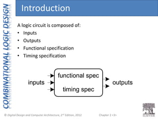
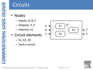
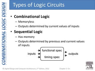
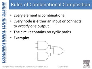
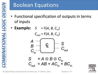
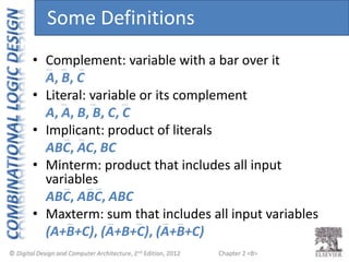
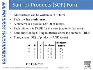
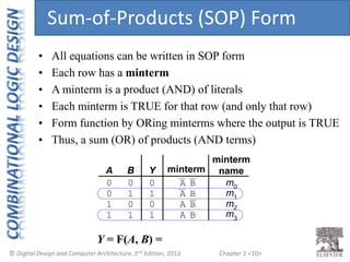
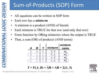
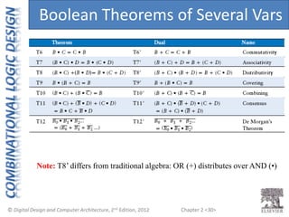
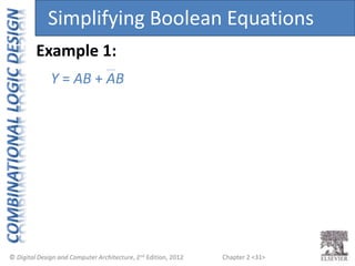
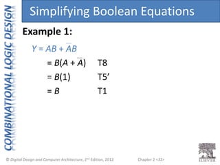
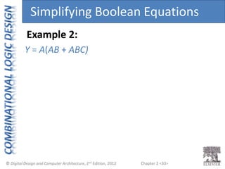
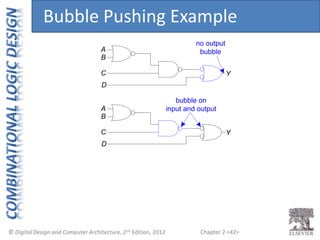
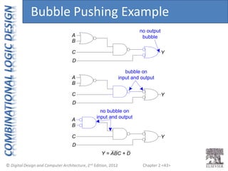
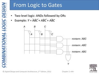
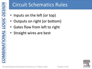
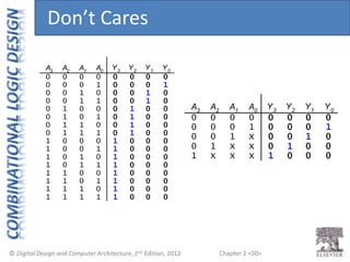
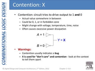
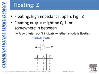
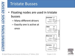
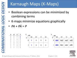
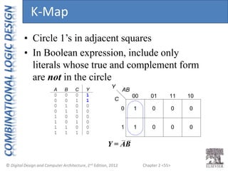
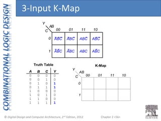
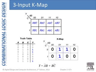
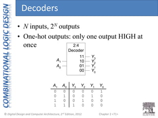
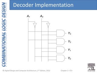
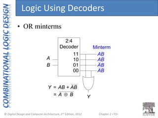
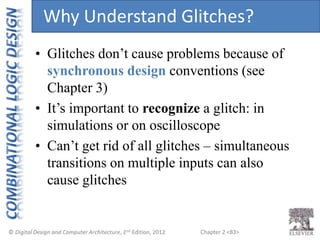
Chapter 2 <1>
Digital Design and Computer Architecture, 2nd Edition
Chapter 2
David Money Harris and Sarah L. Harris
Chapter 2 <2>
• Introduction
• Boolean Equations
• Boolean Algebra
• From Logic to Gates
• Multilevel Combinational Logic
• X’s and Z’s, Oh My
• Karnaugh Maps
• Combinational Building Blocks
• Timing
Chapter 2 :: Topics
Chapter 2 <3>
A logic circuit is composed of:
• Inputs
• Outputs
• Functional specification
• Timing specification
inputs outputs
functional spec
timing spec
Introduction
Chapter 2 <4>
• Nodes
– Inputs: A, B, C
– Outputs: Y, Z
– Internal: n1
• Circuit elements
– E1, E2, E3
– Each a circuit
A E1
E2
E3
B
C
n1
Y
Z
Circuits
Chapter 2 <5>
• Combinational Logic
– Memoryless
– Outputs determined by current values of inputs
• Sequential Logic
– Has memory
– Outputs determined by previous and current values
of inputs
inputs outputs
functional spec
timing spec
Types of Logic Circuits
Chapter 2 <6>
• Every element is combinational
• Every node is either an input or connects
to exactly one output
• The circuit contains no cyclic paths
• Example:
Rules of Combinational Composition
Chapter 2 <7>
• Functional specification of outputs in terms
of inputs
• Example: S = F(A, B, Cin)
Cout = F(A, B, Cin)
A
S
S = A  B  Cin
Cout
= AB + ACin
+ BCin
B
Cin
C
L
Cout
Boolean Equations
Chapter 2 <8>
• Complement: variable with a bar over it
A, B, C
• Literal: variable or its complement
A, A, B, B, C, C
• Implicant: product of literals
ABC, AC, BC
• Minterm: product that includes all input
variables
ABC, ABC, ABC
• Maxterm: sum that includes all input variables
(A+B+C), (A+B+C), (A+B+C)
Some Definitions
Chapter 2 <9>
Y = F(A, B) =
• All equations can be written in SOP form
• Each row has a minterm
• A minterm is a product (AND) of literals
• Each minterm is TRUE for that row (and only that row)
• Form function by ORing minterms where the output is TRUE
• Thus, a sum (OR) of products (AND terms)
Sum-of-Products (SOP) Form
A B Y
0 0
0 1
1 0
1 1
0
1
0
1
minterm
A B
A B
A B
A B
minterm
name
m0
m1
m2
m3
Chapter 2 <10>
Y = F(A, B) =
Sum-of-Products (SOP) Form
• All equations can be written in SOP form
• Each row has a minterm
• A minterm is a product (AND) of literals
• Each minterm is TRUE for that row (and only that row)
• Form function by ORing minterms where the output is TRUE
• Thus, a sum (OR) of products (AND terms)
A B Y
0 0
0 1
1 0
1 1
0
1
0
1
minterm
A B
A B
A B
A B
minterm
name
m0
m1
m2
m3
Chapter 2 <11>
Y = F(A, B) = AB + AB = Σ(1, 3)
Sum-of-Products (SOP) Form
• All equations can be written in SOP form
• Each row has a minterm
• A minterm is a product (AND) of literals
• Each minterm is TRUE for that row (and only that row)
• Form function by ORing minterms where the output is TRUE
• Thus, a sum (OR) of products (AND terms)
A B Y
0 0
0 1
1 0
1 1
0
1
0
1
minterm
A B
A B
A B
A B
minterm
name
m0
m1
m2
m3
Chapter 2 <12>
Y = F(A, B) = (A + B)(A + B) = Π(0, 2)
• All Boolean equations can be written in POS form
• Each row has a maxterm
• A maxterm is a sum (OR) of literals
• Each maxterm is FALSE for that row (and only that row)
• Form function by ANDing the maxterms for which the
output is FALSE
• Thus, a product (AND) of sums (OR terms)
Product-of-Sums (POS) Form
A + B
A B Y
0 0
0 1
1 0
1 1
0
1
0
1
maxterm
A + B
A + B
A + B
maxterm
name
M0
M1
M2
M3
Chapter 2 <13>
• You are going to the cafeteria for lunch
– You won’t eat lunch (E)
– If it’s not open (O) or
– If they only serve corndogs (C)
• Write a truth table for determining if you
will eat lunch (E).
O C E
0 0
0 1
1 0
1 1
Boolean Equations Example
Chapter 2 <14>
• You are going to the cafeteria for lunch
– You won’t eat lunch (E)
– If it’s not open (O) or
– If they only serve corndogs (C)
• Write a truth table for determining if you
will eat lunch (E).
O C E
0 0
0 1
1 0
1 1
0
0
1
0
Boolean Equations Example
Chapter 2 <15>
SOP & POS Form
• SOP – sum-of-products
• POS – product-of-sums
O C E
0 0
0 1
1 0
1 1
minterm
O C
O C
O C
O C
O + C
O C E
0 0
0 1
1 0
1 1
maxterm
O + C
O + C
O + C
Chapter 2 <16>
• SOP – sum-of-products
• POS – product-of-sums
O + C
O C E
0 0
0 1
1 0
1 1
0
0
1
0
maxterm
O + C
O + C
O + C
O C E
0 0
0 1
1 0
1 1
0
0
1
0
minterm
O C
O C
O C
O C
E = (O + C)(O + C)(O + C)
= Π(0, 1, 3)
E = OC
= Σ(2)
SOP & POS Form
Chapter 2 <17>
• Axioms and theorems to simplify Boolean
equations
• Like regular algebra, but simpler: variables
have only two values (1 or 0)
• Duality in axioms and theorems:
– ANDs and ORs, 0’s and 1’s interchanged
Boolean Algebra
Chapter 2 <18>
Boolean Axioms
Chapter 2 <19>
• B 1 = B
• B + 0 = B
T1: Identity Theorem
Chapter 2 <20>
1 =
=
B
0
B
B
B
• B 1 = B
• B + 0 = B
T1: Identity Theorem
Chapter 2 <21>
• B 0 = 0
• B + 1 = 1
T2: Null Element Theorem
Chapter 2 <22>
0 =
=
B
1
B
1
0
• B 0 = 0
• B + 1 = 1
T2: Null Element Theorem
Chapter 2 <23>
• B B = B
• B + B = B
T3: Idempotency Theorem
Chapter 2 <24>
B =
=
B
B
B
B
B
• B B = B
• B + B = B
T3: Idempotency Theorem
Chapter 2 <25>
• B = B
T4: Identity Theorem
Chapter 2 <26>
= B
B
• B = B
T4: Identity Theorem
Chapter 2 <27>
• B B = 0
• B + B = 1
T5: Complement Theorem
Chapter 2 <28>
B =
=
B
B
B
1
0
• B B = 0
• B + B = 1
T5: Complement Theorem
Chapter 2 <29>
Boolean Theorems Summary
Chapter 2 <30>
Boolean Theorems of Several Vars
Note: T8’ differs from traditional algebra: OR (+) distributes over AND (•)
( )
Chapter 2 <31>
Y = AB + AB
Simplifying Boolean Equations
Example 1:
Chapter 2 <32>
Y = AB + AB
= B(A + A) T8
= B(1) T5’
= B T1
Simplifying Boolean Equations
Example 1:
Chapter 2 <33>
Y = A(AB + ABC)
Example 2:
Simplifying Boolean Equations
Chapter 2 <34>
Y = A(AB + ABC)
= A(AB(1 + C)) T8
= A(AB(1)) T2’
= A(AB) T1
= (AA)B T7
= AB T3
Example 2:
Simplifying Boolean Equations
Chapter 2 <35>
• Y = AB = A + B
• Y = A + B = A B
A
B
Y
A
B
Y
A
B
Y
A
B
Y
DeMorgan’s Theorem
Chapter 2 <36>
• Backward:
– Body changes
– Adds bubbles to inputs
• Forward:
– Body changes
– Adds bubble to output
A
B
Y
A
B
Y
A
B
Y
A
B
Y
Bubble Pushing
Chapter 2 <37>
A
B
Y
C
D
• What is the Boolean expression for this
circuit?
Bubble Pushing
Chapter 2 <38>
A
B
Y
C
D
• What is the Boolean expression for this
circuit?
Y = AB + CD
Bubble Pushing
Chapter 2 <39>
A
B
C
D
Y
• Begin at output, then work toward inputs
• Push bubbles on final output back
• Draw gates in a form so bubbles cancel
Bubble Pushing Rules
Chapter 2 <40>
A
B
C Y
D
Bubble Pushing Example
Chapter 2 <41>
A
B
C Y
D
no output
bubble
Bubble Pushing Example
Chapter 2 <42>
bubble on
input and output
A
B
C
D
Y
A
B
C Y
D
no output
bubble
Bubble Pushing Example
Chapter 2 <43>
A
B
C
D
Y
bubble on
input and output
A
B
C
D
Y
A
B
C Y
D
Y = ABC + D
no output
bubble
no bubble on
input and output
Bubble Pushing Example
Chapter 2 <44>
• Two-level logic: ANDs followed by ORs
• Example: Y = ABC + ABC + ABC
B
A C
Y
minterm: ABC
minterm: ABC
minterm: ABC
A B C
From Logic to Gates
Chapter 2 <45>
• Inputs on the left (or top)
• Outputs on right (or bottom)
• Gates flow from left to right
• Straight wires are best
Circuit Schematics Rules
Chapter 2 <46>
• Wires always connect at a T junction
• A dot where wires cross indicates a
connection between the wires
• Wires crossing without a dot make no
connection
wires connect
at a T junction
wires connect
at a dot
wires crossing
without a dot do
not connect
Circuit Schematic Rules (cont.)
Chapter 2 <47>
A1 A0
0 0
0 1
1 0
1 1
Y3 Y2 Y1 Y0
A3 A2
0 0
0 0
0 0
0 0
0 0
0 1
0 1
1 0
1 1
0 0
0 1
0 1
0 1
1 0
0 1
1 0
1 0
1 1
0 0
0 1
1 0
1 0
1 1
1 1
1 0
1 1
1 1
1 1
A0
A1
PRIORITY
CiIRCUIT
A2
A3
Y0
Y1
Y2
Y3
• Example: Priority Circuit
Output asserted
corresponding to
most significant
TRUE input
Multiple-Output Circuits
Chapter 2 <48>
0
A1 A0
0 0
0 1
1 0
1 1
0
0
0
Y3 Y2 Y1 Y0
0
0
0
0
0
0
1
1
0
1
0
0
A3 A2
0 0
0 0
0 0
0 0
0 0 0 1 0 0
0 1
0 1
1 0
1 1
0 0
0 1
0 1
0 1
1 0
0 1
1 0
1 0
1 1
0 0
0 1
1 0
1 0
1 1
1 1
1 0
1 1
1 1
1 1
0
0
0
1
1
1
1
0
0
0
0
0
0
0
0
0
1 0 0 0
1
1
1
1
0
0
0
0
0
0
0
0
0
0
0
0
1 0 0 0
1 0 0 0
A0
A1
PRIORITY
CiIRCUIT
A2
A3
Y0
Y1
Y2
Y3
• Example: Priority Circuit
Output asserted
corresponding to
most significant
TRUE input
Multiple-Output Circuits
Chapter 2 <49>
A1 A0
0 0
0 1
1 0
1 1
0
0
0
0
Y3 Y2 Y1 Y0
0
0
0
0
0
0
1
1
0
1
0
0
A3 A2
0 0
0 0
0 0
0 0
0 0 0 1 0 0
0 1
0 1
1 0
1 1
0 0
0 1
0 1
0 1
1 0
0 1
1 0
1 0
1 1
0 0
0 1
1 0
1 0
1 1
1 1
1 0
1 1
1 1
1 1
0
0
0
1
1
1
1
0
0
0
0
0
0
0
0
0
1 0 0 0
1
1
1
1
0
0
0
0
0
0
0
0
0
0
0
0
1 0 0 0
1 0 0 0
A3
A2
A1
A0
Y3
Y2
Y1
Y0
Priority Circuit Hardware
Chapter 2 <50>
A1 A0
0 0
0 1
1 0
1 1
0
0
0
0
Y3 Y2 Y1 Y0
0
0
0
0
0
0
1
1
0
1
0
0
A3 A2
0 0
0 0
0 0
0 0
0 0 0 1 0 0
0 1
0 1
1 0
1 1
0 0
0 1
0 1
0 1
1 0
0 1
1 0
1 0
1 1
0 0
0 1
1 0
1 0
1 1
1 1
1 0
1 1
1 1
1 1
0
0
0
1
1
1
1
0
0
0
0
0
0
0
0
0
1 0 0 0
1
1
1
1
0
0
0
0
0
0
0
0
0
0
0
0
1 0 0 0
1 0 0 0
A1 A0
0 0
0 1
1 X
X X
0
0
0
0
Y3 Y2 Y1 Y0
0
0
0
1
0
0
1
0
0
1
0
0
A3 A2
0 0
0 0
0 0
0 1
X X 1 0 0 0
1 X
Don’t Cares
Chapter 2 <51>
• Contention: circuit tries to drive output to 1 and 0
– Actual value somewhere in between
– Could be 0, 1, or in forbidden zone
– Might change with voltage, temperature, time, noise
– Often causes excessive power dissipation
• Warnings:
– Contention usually indicates a bug.
– X is used for “don’t care” and contention - look at the context
to tell them apart
A = 1
Y = X
B = 0
Contention: X
Chapter 2 <52>
• Floating, high impedance, open, high Z
• Floating output might be 0, 1, or
somewhere in between
– A voltmeter won’t indicate whether a node is floating
Tristate Buffer
E A Y
0 0 Z
0 1 Z
1 0 0
1 1 1
A
E
Y
Floating: Z
Chapter 2 <53>
• Floating nodes are used in tristate
busses
– Many different drivers
– Exactly one is active at
once
en1
to bus
frombus
en2
to bus
frombus
en3
to bus
frombus
en4
to bus
frombus
shared
bus
processor
video
Ethernet
memory
Tristate Busses
Chapter 2 <54>
• Boolean expressions can be minimized by
combining terms
• K-maps minimize equations graphically
• PA + PA = P
C
00 01
0
1
Y
11 10
AB
1
1
0
0
0
0
0
0
C 00 01
0
1
Y
11 10
AB
ABC
ABC
ABC
ABC
ABC
ABC
ABC
ABC
B C
0 0
0 1
1 0
1 1
A
0
0
0
0
0 0
0 1
1 0
1 1
1
1
1
1
1
1
0
0
0
0
0
0
Y
Karnaugh Maps (K-Maps)
Chapter 2 <55>
C
00 01
0
1
Y
11 10
AB
1
0
0
0
0
0
0
1
B C
0 0
0 1
1 0
1 1
A
0
0
0
0
0 0
0 1
1 0
1 1
1
1
1
1
1
1
0
0
0
0
0
0
Y
• Circle 1’s in adjacent squares
• In Boolean expression, include only
literals whose true and complement form
are not in the circle
Y = AB
K-Map
Chapter 2 <56>
C 00 01
0
1
Y
11 10
AB
ABC
ABC
ABC
ABC
ABC
ABC
ABC
ABC
1
B C Y
0 0 0
0 1 0
1 0
1 1 1
Truth Table
C 00 01
0
1
Y
11 10
AB
A
0
0
0
0
0 0 0
0 1 0
1 0 0
1 1 1
1
1
1
1
K-Map
3-Input K-Map
Chapter 2 <57>
C 00 01
0
1
Y
11 10
AB
ABC
ABC
ABC
ABC
ABC
ABC
ABC
ABC
1 0
B C Y
0 0 0
0 1 0
1 0
1 1 1
Truth Table
C 00 01
0
1
Y
11 10
AB
A
0
0
0
0
0 0 0
0 1 0
1 0 0
1 1 1
1
1
1
1
0
1
1
1
0
0
0
K-Map
Y = AB + BC
3-Input K-Map
Chapter 2 <58>
• Complement: variable with a bar over it
A, B, C
• Literal: variable or its complement
A, A, B, B, C, C
• Implicant: product of literals
ABC, AC, BC
• Prime implicant: implicant corresponding to
the largest circle in a K-map
K-Map Definitions
Chapter 2 <59>
• Every 1 must be circled at least once
• Each circle must span a power of 2 (i.e. 1, 2,
4) squares in each direction
• Each circle must be as large as possible
• A circle may wrap around the edges
• A “don't care” (X) is circled only if it helps
minimize the equation
K-Map Rules
Chapter 2 <60>
01 11
01
11
10
00
00
10
AB
CD
Y
0
C D
0 0
0 1
1 0
1 1
B
0
0
0
0
0 0
0 1
1 0
1 1
1
1
1
1
1
1
1
0
1
1
1
Y
A
0
0
0
0
0
0
0
0
0 0
0 1
1 0
1 1
0
0
0
0
0 0
0 1
1 0
1 1
1
1
1
1
1
1
1
1
1
1
1
1
1
1
1
0
0
0
0
0
4-Input K-Map
Chapter 2 <61>
01 11
1
0
0
1
0
0
1
1
01
1
1
1
1
0
0
0
1
11
10
00
00
10
AB
CD
Y
0
C D
0 0
0 1
1 0
1 1
B
0
0
0
0
0 0
0 1
1 0
1 1
1
1
1
1
1
1
1
0
1
1
1
Y
A
0
0
0
0
0
0
0
0
0 0
0 1
1 0
1 1
0
0
0
0
0 0
0 1
1 0
1 1
1
1
1
1
1
1
1
1
1
1
1
1
1
1
1
0
0
0
0
0
4-Input K-Map
Chapter 2 <62>
01 11
1
0
0
1
0
0
1
1
01
1
1
1
1
0
0
0
1
11
10
00
00
10
AB
CD
Y
Y = AC + ABD + ABC + BD
0
C D
0 0
0 1
1 0
1 1
B
0
0
0
0
0 0
0 1
1 0
1 1
1
1
1
1
1
1
1
0
1
1
1
Y
A
0
0
0
0
0
0
0
0
0 0
0 1
1 0
1 1
0
0
0
0
0 0
0 1
1 0
1 1
1
1
1
1
1
1
1
1
1
1
1
1
1
1
1
0
0
0
0
0
4-Input K-Map
Chapter 2 <63>
0
C D
0 0
0 1
1 0
1 1
B
0
0
0
0
0 0
0 1
1 0
1 1
1
1
1
1
1
1
1
0
X
1
1
Y
A
0
0
0
0
0
0
0
0
0 0
0 1
1 0
1 1
0
0
0
0
0 0
0 1
1 0
1 1
1
1
1
1
1
1
1
1
1
1
1
1
1
1
X
X
X
X
X
X
01 11
01
11
10
00
00
10
AB
CD
Y
K-Maps with Don’t Cares
Chapter 2 <64>
0
C D
0 0
0 1
1 0
1 1
B
0
0
0
0
0 0
0 1
1 0
1 1
1
1
1
1
1
1
1
0
X
1
1
Y
A
0
0
0
0
0
0
0
0
0 0
0 1
1 0
1 1
0
0
0
0
0 0
0 1
1 0
1 1
1
1
1
1
1
1
1
1
1
1
1
1
1
1
X
X
X
X
X
X
01 11
1
0
0
X
X
X
1
1
01
1
1
1
1
X
X
X
X
11
10
00
00
10
AB
CD
Y
K-Maps with Don’t Cares
Chapter 2 <65>
0
C D
0 0
0 1
1 0
1 1
B
0
0
0
0
0 0
0 1
1 0
1 1
1
1
1
1
1
1
1
0
X
1
1
Y
A
0
0
0
0
0
0
0
0
0 0
0 1
1 0
1 1
0
0
0
0
0 0
0 1
1 0
1 1
1
1
1
1
1
1
1
1
1
1
1
1
1
1
X
X
X
X
X
X
01 11
1
0
0
X
X
X
1
1
01
1
1
1
1
X
X
X
X
11
10
00
00
10
AB
CD
Y
Y = A + BD + C
K-Maps with Don’t Cares
Chapter 2 <66>
• Multiplexers
• Decoders
Combinational Building Blocks
Chapter 2 <67>
• Selects between one of N inputs to connect
to output
• log2N-bit select input – control input
• Example: 2:1 Mux
Multiplexer (Mux)
Y
0 0
0 1
1 0
1 1
0
1
0
1
0
0
0
0
0 0
0 1
1 0
1 1
1
1
1
1
0
0
1
1
0
1
S
D0
Y
D1
D1 D0
S Y
0
1 D1
D0
S
Chapter 2 <68>
2-<68>
• Logic gates
– Sum-of-products form
Y
D0
S
D1
D1
Y
D0
S
S
00 01
0
1
Y
11 10
D0
D1
0
0
0
1
1
1
1
0
Y = D0
S + D1
S
• Tristates
– For an N-input mux, use N
tristates
– Turn on exactly one to
select the appropriate input
Multiplexer Implementations
Chapter 2 <69>
A B Y
0 0 0
0 1 0
1 0 0
1 1 1
Y = AB
00
Y
01
10
11
A B
• Using the mux as a lookup table
Logic using Multiplexers
Chapter 2 <70>
A B Y
0 0 0
0 1 0
1 0 0
1 1 1
Y = AB
A Y
0
1
0 0
1
A
B
Y
B
• Reducing the size of the mux
Logic using Multiplexers
Chapter 2 <71>
2:4
Decoder
A1
A0
Y3
Y2
Y1
Y0
00
01
10
11
0 0
0 1
1 0
1 1
0
0
0
1
Y3
Y2
Y1
Y0
A0
A1
0
0
1
0
0
1
0
0
1
0
0
0
• N inputs, 2N outputs
• One-hot outputs: only one output HIGH at
once
Decoders
Chapter 2 <72>
Y3
Y2
Y1
Y0
A0
A1
Decoder Implementation
Chapter 2 <73>
2:4
Decoder
A
B
00
01
10
11
Y = AB + AB
Y
AB
AB
AB
AB
Minterm
= A  B
• OR minterms
Logic Using Decoders
Chapter 2 <74>
ENOUGH FOR TODAY!
Chapter 2 <75>
A
Y
Time
delay
A Y
• Delay between input change and output
changing
• How to build fast circuits?
Timing
Chapter 2 <76>
A
Y
Time
A Y
tpd
tcd
• Propagation delay: tpd = max delay from input to output
• Contamination delay: tcd = min delay from input to
output
Propagation & Contamination Delay
Chapter 2 <77>
• Delay is caused by
– Capacitance and resistance in a circuit
– Speed of light limitation
• Reasons why tpd and tcd may be different:
– Different rising and falling delays
– Multiple inputs and outputs, some of which are
faster than others
– Circuits slow down when hot and speed up when
cold
Propagation & Contamination Delay
Chapter 2 <78>
A
B
C
D Y
Critical Path
Short Path
n1
n2
Critical (Long) Path: tpd = 2tpd_AND + tpd_OR
Short Path: tcd = tcd_AND
Critical (Long) & Short Paths
Chapter 2 <79>
• When a single input change causes an output
to change multiple times
Glitches
Chapter 2 <80>
A
B
C
Y
00 01
1
Y
11 10
AB
1
1
0
1
0
1
0
0
C
0
Y = AB + BC
• What happens when A = 0, C = 1, B falls?
Glitch Example
Chapter 2 <81>
A = 0
B = 1 0
C = 1
Y = 1 0 1
Short Path
Critical Path
B
Y
Time
1 0
0 1
glitch
n1
n2
n2
n1
Glitch Example (cont.)
Chapter 2 <82>
00 01
1
Y
11 10
AB
1
1
0
1
0
1
0
0
C
0
Y = AB + BC + AC
AC
B = 1 0
Y = 1
A = 0
C = 1
Fixing the Glitch
Chapter 2 <83>
• Glitches don’t cause problems because of
synchronous design conventions (see
Chapter 3)
• It’s important to recognize a glitch: in
simulations or on oscilloscope
• Can’t get rid of all glitches – simultaneous
transitions on multiple inputs can also
cause glitches
Why Understand Glitches?

Bubble pushing.pptx

  • 1.
    Chapter 2 <1> DigitalDesign and Computer Architecture, 2nd Edition Chapter 2 David Money Harris and Sarah L. Harris
  • 2.
    Chapter 2 <2> •Introduction • Boolean Equations • Boolean Algebra • From Logic to Gates • Multilevel Combinational Logic • X’s and Z’s, Oh My • Karnaugh Maps • Combinational Building Blocks • Timing Chapter 2 :: Topics
  • 3.
    Chapter 2 <3> Alogic circuit is composed of: • Inputs • Outputs • Functional specification • Timing specification inputs outputs functional spec timing spec Introduction
  • 4.
    Chapter 2 <4> •Nodes – Inputs: A, B, C – Outputs: Y, Z – Internal: n1 • Circuit elements – E1, E2, E3 – Each a circuit A E1 E2 E3 B C n1 Y Z Circuits
  • 5.
    Chapter 2 <5> •Combinational Logic – Memoryless – Outputs determined by current values of inputs • Sequential Logic – Has memory – Outputs determined by previous and current values of inputs inputs outputs functional spec timing spec Types of Logic Circuits
  • 6.
    Chapter 2 <6> •Every element is combinational • Every node is either an input or connects to exactly one output • The circuit contains no cyclic paths • Example: Rules of Combinational Composition
  • 7.
    Chapter 2 <7> •Functional specification of outputs in terms of inputs • Example: S = F(A, B, Cin) Cout = F(A, B, Cin) A S S = A  B  Cin Cout = AB + ACin + BCin B Cin C L Cout Boolean Equations
  • 8.
    Chapter 2 <8> •Complement: variable with a bar over it A, B, C • Literal: variable or its complement A, A, B, B, C, C • Implicant: product of literals ABC, AC, BC • Minterm: product that includes all input variables ABC, ABC, ABC • Maxterm: sum that includes all input variables (A+B+C), (A+B+C), (A+B+C) Some Definitions
  • 9.
    Chapter 2 <9> Y= F(A, B) = • All equations can be written in SOP form • Each row has a minterm • A minterm is a product (AND) of literals • Each minterm is TRUE for that row (and only that row) • Form function by ORing minterms where the output is TRUE • Thus, a sum (OR) of products (AND terms) Sum-of-Products (SOP) Form A B Y 0 0 0 1 1 0 1 1 0 1 0 1 minterm A B A B A B A B minterm name m0 m1 m2 m3
  • 10.
    Chapter 2 <10> Y= F(A, B) = Sum-of-Products (SOP) Form • All equations can be written in SOP form • Each row has a minterm • A minterm is a product (AND) of literals • Each minterm is TRUE for that row (and only that row) • Form function by ORing minterms where the output is TRUE • Thus, a sum (OR) of products (AND terms) A B Y 0 0 0 1 1 0 1 1 0 1 0 1 minterm A B A B A B A B minterm name m0 m1 m2 m3
  • 11.
    Chapter 2 <11> Y= F(A, B) = AB + AB = Σ(1, 3) Sum-of-Products (SOP) Form • All equations can be written in SOP form • Each row has a minterm • A minterm is a product (AND) of literals • Each minterm is TRUE for that row (and only that row) • Form function by ORing minterms where the output is TRUE • Thus, a sum (OR) of products (AND terms) A B Y 0 0 0 1 1 0 1 1 0 1 0 1 minterm A B A B A B A B minterm name m0 m1 m2 m3
  • 12.
    Chapter 2 <12> Y= F(A, B) = (A + B)(A + B) = Π(0, 2) • All Boolean equations can be written in POS form • Each row has a maxterm • A maxterm is a sum (OR) of literals • Each maxterm is FALSE for that row (and only that row) • Form function by ANDing the maxterms for which the output is FALSE • Thus, a product (AND) of sums (OR terms) Product-of-Sums (POS) Form A + B A B Y 0 0 0 1 1 0 1 1 0 1 0 1 maxterm A + B A + B A + B maxterm name M0 M1 M2 M3
  • 13.
    Chapter 2 <13> •You are going to the cafeteria for lunch – You won’t eat lunch (E) – If it’s not open (O) or – If they only serve corndogs (C) • Write a truth table for determining if you will eat lunch (E). O C E 0 0 0 1 1 0 1 1 Boolean Equations Example
  • 14.
    Chapter 2 <14> •You are going to the cafeteria for lunch – You won’t eat lunch (E) – If it’s not open (O) or – If they only serve corndogs (C) • Write a truth table for determining if you will eat lunch (E). O C E 0 0 0 1 1 0 1 1 0 0 1 0 Boolean Equations Example
  • 15.
    Chapter 2 <15> SOP& POS Form • SOP – sum-of-products • POS – product-of-sums O C E 0 0 0 1 1 0 1 1 minterm O C O C O C O C O + C O C E 0 0 0 1 1 0 1 1 maxterm O + C O + C O + C
  • 16.
    Chapter 2 <16> •SOP – sum-of-products • POS – product-of-sums O + C O C E 0 0 0 1 1 0 1 1 0 0 1 0 maxterm O + C O + C O + C O C E 0 0 0 1 1 0 1 1 0 0 1 0 minterm O C O C O C O C E = (O + C)(O + C)(O + C) = Π(0, 1, 3) E = OC = Σ(2) SOP & POS Form
  • 17.
    Chapter 2 <17> •Axioms and theorems to simplify Boolean equations • Like regular algebra, but simpler: variables have only two values (1 or 0) • Duality in axioms and theorems: – ANDs and ORs, 0’s and 1’s interchanged Boolean Algebra
  • 18.
  • 19.
    Chapter 2 <19> •B 1 = B • B + 0 = B T1: Identity Theorem
  • 20.
    Chapter 2 <20> 1= = B 0 B B B • B 1 = B • B + 0 = B T1: Identity Theorem
  • 21.
    Chapter 2 <21> •B 0 = 0 • B + 1 = 1 T2: Null Element Theorem
  • 22.
    Chapter 2 <22> 0= = B 1 B 1 0 • B 0 = 0 • B + 1 = 1 T2: Null Element Theorem
  • 23.
    Chapter 2 <23> •B B = B • B + B = B T3: Idempotency Theorem
  • 24.
    Chapter 2 <24> B= = B B B B B • B B = B • B + B = B T3: Idempotency Theorem
  • 25.
    Chapter 2 <25> •B = B T4: Identity Theorem
  • 26.
    Chapter 2 <26> =B B • B = B T4: Identity Theorem
  • 27.
    Chapter 2 <27> •B B = 0 • B + B = 1 T5: Complement Theorem
  • 28.
    Chapter 2 <28> B= = B B B 1 0 • B B = 0 • B + B = 1 T5: Complement Theorem
  • 29.
    Chapter 2 <29> BooleanTheorems Summary
  • 30.
    Chapter 2 <30> BooleanTheorems of Several Vars Note: T8’ differs from traditional algebra: OR (+) distributes over AND (•) ( )
  • 31.
    Chapter 2 <31> Y= AB + AB Simplifying Boolean Equations Example 1:
  • 32.
    Chapter 2 <32> Y= AB + AB = B(A + A) T8 = B(1) T5’ = B T1 Simplifying Boolean Equations Example 1:
  • 33.
    Chapter 2 <33> Y= A(AB + ABC) Example 2: Simplifying Boolean Equations
  • 34.
    Chapter 2 <34> Y= A(AB + ABC) = A(AB(1 + C)) T8 = A(AB(1)) T2’ = A(AB) T1 = (AA)B T7 = AB T3 Example 2: Simplifying Boolean Equations
  • 35.
    Chapter 2 <35> •Y = AB = A + B • Y = A + B = A B A B Y A B Y A B Y A B Y DeMorgan’s Theorem
  • 36.
    Chapter 2 <36> •Backward: – Body changes – Adds bubbles to inputs • Forward: – Body changes – Adds bubble to output A B Y A B Y A B Y A B Y Bubble Pushing
  • 37.
    Chapter 2 <37> A B Y C D •What is the Boolean expression for this circuit? Bubble Pushing
  • 38.
    Chapter 2 <38> A B Y C D •What is the Boolean expression for this circuit? Y = AB + CD Bubble Pushing
  • 39.
    Chapter 2 <39> A B C D Y •Begin at output, then work toward inputs • Push bubbles on final output back • Draw gates in a form so bubbles cancel Bubble Pushing Rules
  • 40.
    Chapter 2 <40> A B CY D Bubble Pushing Example
  • 41.
    Chapter 2 <41> A B CY D no output bubble Bubble Pushing Example
  • 42.
    Chapter 2 <42> bubbleon input and output A B C D Y A B C Y D no output bubble Bubble Pushing Example
  • 43.
    Chapter 2 <43> A B C D Y bubbleon input and output A B C D Y A B C Y D Y = ABC + D no output bubble no bubble on input and output Bubble Pushing Example
  • 44.
    Chapter 2 <44> •Two-level logic: ANDs followed by ORs • Example: Y = ABC + ABC + ABC B A C Y minterm: ABC minterm: ABC minterm: ABC A B C From Logic to Gates
  • 45.
    Chapter 2 <45> •Inputs on the left (or top) • Outputs on right (or bottom) • Gates flow from left to right • Straight wires are best Circuit Schematics Rules
  • 46.
    Chapter 2 <46> •Wires always connect at a T junction • A dot where wires cross indicates a connection between the wires • Wires crossing without a dot make no connection wires connect at a T junction wires connect at a dot wires crossing without a dot do not connect Circuit Schematic Rules (cont.)
  • 47.
    Chapter 2 <47> A1A0 0 0 0 1 1 0 1 1 Y3 Y2 Y1 Y0 A3 A2 0 0 0 0 0 0 0 0 0 0 0 1 0 1 1 0 1 1 0 0 0 1 0 1 0 1 1 0 0 1 1 0 1 0 1 1 0 0 0 1 1 0 1 0 1 1 1 1 1 0 1 1 1 1 1 1 A0 A1 PRIORITY CiIRCUIT A2 A3 Y0 Y1 Y2 Y3 • Example: Priority Circuit Output asserted corresponding to most significant TRUE input Multiple-Output Circuits
  • 48.
    Chapter 2 <48> 0 A1A0 0 0 0 1 1 0 1 1 0 0 0 Y3 Y2 Y1 Y0 0 0 0 0 0 0 1 1 0 1 0 0 A3 A2 0 0 0 0 0 0 0 0 0 0 0 1 0 0 0 1 0 1 1 0 1 1 0 0 0 1 0 1 0 1 1 0 0 1 1 0 1 0 1 1 0 0 0 1 1 0 1 0 1 1 1 1 1 0 1 1 1 1 1 1 0 0 0 1 1 1 1 0 0 0 0 0 0 0 0 0 1 0 0 0 1 1 1 1 0 0 0 0 0 0 0 0 0 0 0 0 1 0 0 0 1 0 0 0 A0 A1 PRIORITY CiIRCUIT A2 A3 Y0 Y1 Y2 Y3 • Example: Priority Circuit Output asserted corresponding to most significant TRUE input Multiple-Output Circuits
  • 49.
    Chapter 2 <49> A1A0 0 0 0 1 1 0 1 1 0 0 0 0 Y3 Y2 Y1 Y0 0 0 0 0 0 0 1 1 0 1 0 0 A3 A2 0 0 0 0 0 0 0 0 0 0 0 1 0 0 0 1 0 1 1 0 1 1 0 0 0 1 0 1 0 1 1 0 0 1 1 0 1 0 1 1 0 0 0 1 1 0 1 0 1 1 1 1 1 0 1 1 1 1 1 1 0 0 0 1 1 1 1 0 0 0 0 0 0 0 0 0 1 0 0 0 1 1 1 1 0 0 0 0 0 0 0 0 0 0 0 0 1 0 0 0 1 0 0 0 A3 A2 A1 A0 Y3 Y2 Y1 Y0 Priority Circuit Hardware
  • 50.
    Chapter 2 <50> A1A0 0 0 0 1 1 0 1 1 0 0 0 0 Y3 Y2 Y1 Y0 0 0 0 0 0 0 1 1 0 1 0 0 A3 A2 0 0 0 0 0 0 0 0 0 0 0 1 0 0 0 1 0 1 1 0 1 1 0 0 0 1 0 1 0 1 1 0 0 1 1 0 1 0 1 1 0 0 0 1 1 0 1 0 1 1 1 1 1 0 1 1 1 1 1 1 0 0 0 1 1 1 1 0 0 0 0 0 0 0 0 0 1 0 0 0 1 1 1 1 0 0 0 0 0 0 0 0 0 0 0 0 1 0 0 0 1 0 0 0 A1 A0 0 0 0 1 1 X X X 0 0 0 0 Y3 Y2 Y1 Y0 0 0 0 1 0 0 1 0 0 1 0 0 A3 A2 0 0 0 0 0 0 0 1 X X 1 0 0 0 1 X Don’t Cares
  • 51.
    Chapter 2 <51> •Contention: circuit tries to drive output to 1 and 0 – Actual value somewhere in between – Could be 0, 1, or in forbidden zone – Might change with voltage, temperature, time, noise – Often causes excessive power dissipation • Warnings: – Contention usually indicates a bug. – X is used for “don’t care” and contention - look at the context to tell them apart A = 1 Y = X B = 0 Contention: X
  • 52.
    Chapter 2 <52> •Floating, high impedance, open, high Z • Floating output might be 0, 1, or somewhere in between – A voltmeter won’t indicate whether a node is floating Tristate Buffer E A Y 0 0 Z 0 1 Z 1 0 0 1 1 1 A E Y Floating: Z
  • 53.
    Chapter 2 <53> •Floating nodes are used in tristate busses – Many different drivers – Exactly one is active at once en1 to bus frombus en2 to bus frombus en3 to bus frombus en4 to bus frombus shared bus processor video Ethernet memory Tristate Busses
  • 54.
    Chapter 2 <54> •Boolean expressions can be minimized by combining terms • K-maps minimize equations graphically • PA + PA = P C 00 01 0 1 Y 11 10 AB 1 1 0 0 0 0 0 0 C 00 01 0 1 Y 11 10 AB ABC ABC ABC ABC ABC ABC ABC ABC B C 0 0 0 1 1 0 1 1 A 0 0 0 0 0 0 0 1 1 0 1 1 1 1 1 1 1 1 0 0 0 0 0 0 Y Karnaugh Maps (K-Maps)
  • 55.
    Chapter 2 <55> C 0001 0 1 Y 11 10 AB 1 0 0 0 0 0 0 1 B C 0 0 0 1 1 0 1 1 A 0 0 0 0 0 0 0 1 1 0 1 1 1 1 1 1 1 1 0 0 0 0 0 0 Y • Circle 1’s in adjacent squares • In Boolean expression, include only literals whose true and complement form are not in the circle Y = AB K-Map
  • 56.
    Chapter 2 <56> C00 01 0 1 Y 11 10 AB ABC ABC ABC ABC ABC ABC ABC ABC 1 B C Y 0 0 0 0 1 0 1 0 1 1 1 Truth Table C 00 01 0 1 Y 11 10 AB A 0 0 0 0 0 0 0 0 1 0 1 0 0 1 1 1 1 1 1 1 K-Map 3-Input K-Map
  • 57.
    Chapter 2 <57> C00 01 0 1 Y 11 10 AB ABC ABC ABC ABC ABC ABC ABC ABC 1 0 B C Y 0 0 0 0 1 0 1 0 1 1 1 Truth Table C 00 01 0 1 Y 11 10 AB A 0 0 0 0 0 0 0 0 1 0 1 0 0 1 1 1 1 1 1 1 0 1 1 1 0 0 0 K-Map Y = AB + BC 3-Input K-Map
  • 58.
    Chapter 2 <58> •Complement: variable with a bar over it A, B, C • Literal: variable or its complement A, A, B, B, C, C • Implicant: product of literals ABC, AC, BC • Prime implicant: implicant corresponding to the largest circle in a K-map K-Map Definitions
  • 59.
    Chapter 2 <59> •Every 1 must be circled at least once • Each circle must span a power of 2 (i.e. 1, 2, 4) squares in each direction • Each circle must be as large as possible • A circle may wrap around the edges • A “don't care” (X) is circled only if it helps minimize the equation K-Map Rules
  • 60.
    Chapter 2 <60> 0111 01 11 10 00 00 10 AB CD Y 0 C D 0 0 0 1 1 0 1 1 B 0 0 0 0 0 0 0 1 1 0 1 1 1 1 1 1 1 1 1 0 1 1 1 Y A 0 0 0 0 0 0 0 0 0 0 0 1 1 0 1 1 0 0 0 0 0 0 0 1 1 0 1 1 1 1 1 1 1 1 1 1 1 1 1 1 1 1 1 0 0 0 0 0 4-Input K-Map
  • 61.
    Chapter 2 <61> 0111 1 0 0 1 0 0 1 1 01 1 1 1 1 0 0 0 1 11 10 00 00 10 AB CD Y 0 C D 0 0 0 1 1 0 1 1 B 0 0 0 0 0 0 0 1 1 0 1 1 1 1 1 1 1 1 1 0 1 1 1 Y A 0 0 0 0 0 0 0 0 0 0 0 1 1 0 1 1 0 0 0 0 0 0 0 1 1 0 1 1 1 1 1 1 1 1 1 1 1 1 1 1 1 1 1 0 0 0 0 0 4-Input K-Map
  • 62.
    Chapter 2 <62> 0111 1 0 0 1 0 0 1 1 01 1 1 1 1 0 0 0 1 11 10 00 00 10 AB CD Y Y = AC + ABD + ABC + BD 0 C D 0 0 0 1 1 0 1 1 B 0 0 0 0 0 0 0 1 1 0 1 1 1 1 1 1 1 1 1 0 1 1 1 Y A 0 0 0 0 0 0 0 0 0 0 0 1 1 0 1 1 0 0 0 0 0 0 0 1 1 0 1 1 1 1 1 1 1 1 1 1 1 1 1 1 1 1 1 0 0 0 0 0 4-Input K-Map
  • 63.
    Chapter 2 <63> 0 CD 0 0 0 1 1 0 1 1 B 0 0 0 0 0 0 0 1 1 0 1 1 1 1 1 1 1 1 1 0 X 1 1 Y A 0 0 0 0 0 0 0 0 0 0 0 1 1 0 1 1 0 0 0 0 0 0 0 1 1 0 1 1 1 1 1 1 1 1 1 1 1 1 1 1 1 1 X X X X X X 01 11 01 11 10 00 00 10 AB CD Y K-Maps with Don’t Cares
  • 64.
    Chapter 2 <64> 0 CD 0 0 0 1 1 0 1 1 B 0 0 0 0 0 0 0 1 1 0 1 1 1 1 1 1 1 1 1 0 X 1 1 Y A 0 0 0 0 0 0 0 0 0 0 0 1 1 0 1 1 0 0 0 0 0 0 0 1 1 0 1 1 1 1 1 1 1 1 1 1 1 1 1 1 1 1 X X X X X X 01 11 1 0 0 X X X 1 1 01 1 1 1 1 X X X X 11 10 00 00 10 AB CD Y K-Maps with Don’t Cares
  • 65.
    Chapter 2 <65> 0 CD 0 0 0 1 1 0 1 1 B 0 0 0 0 0 0 0 1 1 0 1 1 1 1 1 1 1 1 1 0 X 1 1 Y A 0 0 0 0 0 0 0 0 0 0 0 1 1 0 1 1 0 0 0 0 0 0 0 1 1 0 1 1 1 1 1 1 1 1 1 1 1 1 1 1 1 1 X X X X X X 01 11 1 0 0 X X X 1 1 01 1 1 1 1 X X X X 11 10 00 00 10 AB CD Y Y = A + BD + C K-Maps with Don’t Cares
  • 66.
    Chapter 2 <66> •Multiplexers • Decoders Combinational Building Blocks
  • 67.
    Chapter 2 <67> •Selects between one of N inputs to connect to output • log2N-bit select input – control input • Example: 2:1 Mux Multiplexer (Mux) Y 0 0 0 1 1 0 1 1 0 1 0 1 0 0 0 0 0 0 0 1 1 0 1 1 1 1 1 1 0 0 1 1 0 1 S D0 Y D1 D1 D0 S Y 0 1 D1 D0 S
  • 68.
    Chapter 2 <68> 2-<68> •Logic gates – Sum-of-products form Y D0 S D1 D1 Y D0 S S 00 01 0 1 Y 11 10 D0 D1 0 0 0 1 1 1 1 0 Y = D0 S + D1 S • Tristates – For an N-input mux, use N tristates – Turn on exactly one to select the appropriate input Multiplexer Implementations
  • 69.
    Chapter 2 <69> AB Y 0 0 0 0 1 0 1 0 0 1 1 1 Y = AB 00 Y 01 10 11 A B • Using the mux as a lookup table Logic using Multiplexers
  • 70.
    Chapter 2 <70> AB Y 0 0 0 0 1 0 1 0 0 1 1 1 Y = AB A Y 0 1 0 0 1 A B Y B • Reducing the size of the mux Logic using Multiplexers
  • 71.
    Chapter 2 <71> 2:4 Decoder A1 A0 Y3 Y2 Y1 Y0 00 01 10 11 00 0 1 1 0 1 1 0 0 0 1 Y3 Y2 Y1 Y0 A0 A1 0 0 1 0 0 1 0 0 1 0 0 0 • N inputs, 2N outputs • One-hot outputs: only one output HIGH at once Decoders
  • 72.
  • 73.
    Chapter 2 <73> 2:4 Decoder A B 00 01 10 11 Y= AB + AB Y AB AB AB AB Minterm = A  B • OR minterms Logic Using Decoders
  • 74.
  • 75.
    Chapter 2 <75> A Y Time delay AY • Delay between input change and output changing • How to build fast circuits? Timing
  • 76.
    Chapter 2 <76> A Y Time AY tpd tcd • Propagation delay: tpd = max delay from input to output • Contamination delay: tcd = min delay from input to output Propagation & Contamination Delay
  • 77.
    Chapter 2 <77> •Delay is caused by – Capacitance and resistance in a circuit – Speed of light limitation • Reasons why tpd and tcd may be different: – Different rising and falling delays – Multiple inputs and outputs, some of which are faster than others – Circuits slow down when hot and speed up when cold Propagation & Contamination Delay
  • 78.
    Chapter 2 <78> A B C DY Critical Path Short Path n1 n2 Critical (Long) Path: tpd = 2tpd_AND + tpd_OR Short Path: tcd = tcd_AND Critical (Long) & Short Paths
  • 79.
    Chapter 2 <79> •When a single input change causes an output to change multiple times Glitches
  • 80.
    Chapter 2 <80> A B C Y 0001 1 Y 11 10 AB 1 1 0 1 0 1 0 0 C 0 Y = AB + BC • What happens when A = 0, C = 1, B falls? Glitch Example
  • 81.
    Chapter 2 <81> A= 0 B = 1 0 C = 1 Y = 1 0 1 Short Path Critical Path B Y Time 1 0 0 1 glitch n1 n2 n2 n1 Glitch Example (cont.)
  • 82.
    Chapter 2 <82> 0001 1 Y 11 10 AB 1 1 0 1 0 1 0 0 C 0 Y = AB + BC + AC AC B = 1 0 Y = 1 A = 0 C = 1 Fixing the Glitch
  • 83.
    Chapter 2 <83> •Glitches don’t cause problems because of synchronous design conventions (see Chapter 3) • It’s important to recognize a glitch: in simulations or on oscilloscope • Can’t get rid of all glitches – simultaneous transitions on multiple inputs can also cause glitches Why Understand Glitches?