Download as PDF, PPTX

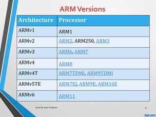
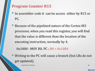
![The Cortex-M3 uses a full - descending stack
arrangement.
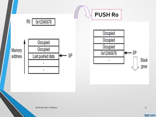
PUSH {R0} ; R13=R13-4, then Memory[R13] = R0
POP {R0} ; R0 = Memory[R13], then R13 = R13 + 4
Multiple registers can also be stored in SP
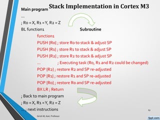
subroutine_1
PUSH {R0-R7, R12, R14} ; Save registers
. . . .………….... . . . .. . .. . .. . . ; Do your processing
POP {R0-R7, R12, R14} ; Restore registers
BX R14 ; Return to calling function
Instead of using R13, SP can be used in program codes
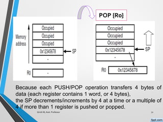
Girish M, Asst. Professor 36](https://image.slidesharecdn.com/gmarmpptmodule-1-200313061108/85/ARM-Microcontrollers-and-Embedded-Systems-Module-1_VTU-36-320.jpg)
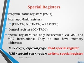
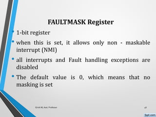
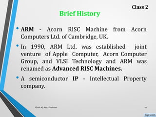
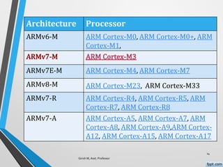
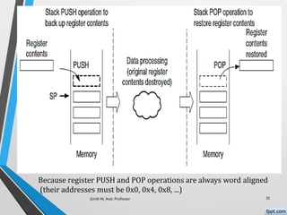
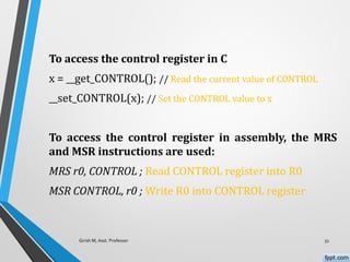
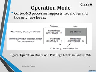
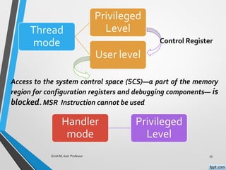
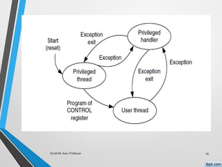
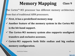
![The Control Register
• The control register has 2 bits
• This is used to define the privilege level and the SP
selection
Girish M, Asst. Professor 50
Bit Function
CONTROL[1] Stack status:
1 = Alternate stack is used
0 = Default stack (MSP) is used
CONTROL[0] 0 = Privileged in thread mode
1 = User state in thread mode](https://image.slidesharecdn.com/gmarmpptmodule-1-200313061108/85/ARM-Microcontrollers-and-Embedded-Systems-Module-1_VTU-50-320.jpg)

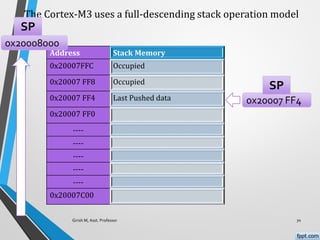
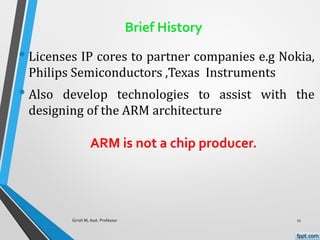
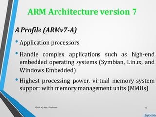
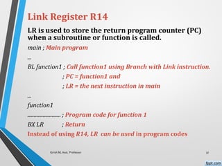
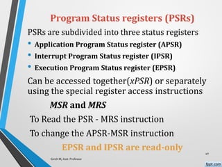
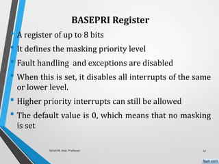
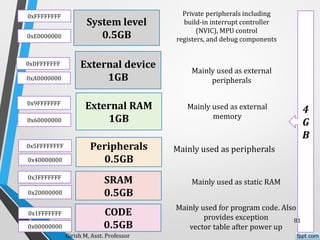
![The two-stack model in the cortex-m3
Girish M, Asst. Professor 73
CONTROL [1]
0 MSP is used for both thread mode
and handler mode
1 PSP is used in thread mode
MSP is used in handler mode
• Cortex-M3 has two SPs: the MSP and the PSP.
• When CONTROL[1] is 0 - same stack memory region
• When the CONTROL[1] is 1 - separate stack memory
regions
Class 8](https://image.slidesharecdn.com/gmarmpptmodule-1-200313061108/85/ARM-Microcontrollers-and-Embedded-Systems-Module-1_VTU-73-320.jpg)
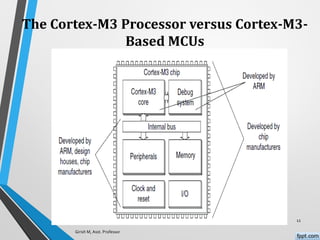
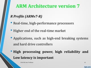
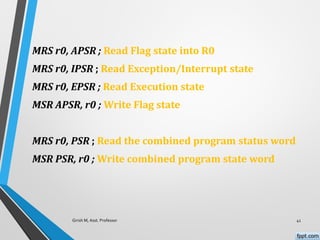
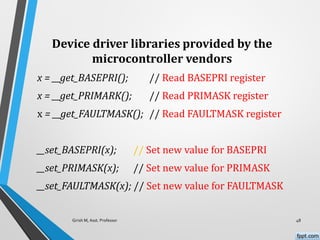
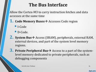
![The two-stack model in the cortex-m3
Girish M, Asst. Professor 74
CONTROL
[1]
0 MSP is used for both thread mode and
handler mode](https://image.slidesharecdn.com/gmarmpptmodule-1-200313061108/85/ARM-Microcontrollers-and-Embedded-Systems-Module-1_VTU-74-320.jpg)
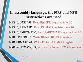
![The two-stack model in the cortex-m3
Girish M, Asst. Professor 75
CONTROL
[1] 1 PSP is used in thread mode
MSP is used in handler mode](https://image.slidesharecdn.com/gmarmpptmodule-1-200313061108/85/ARM-Microcontrollers-and-Embedded-Systems-Module-1_VTU-75-320.jpg)


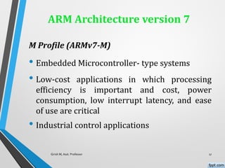
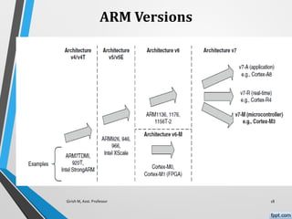
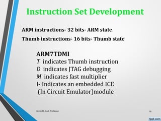
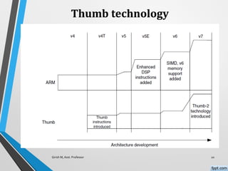
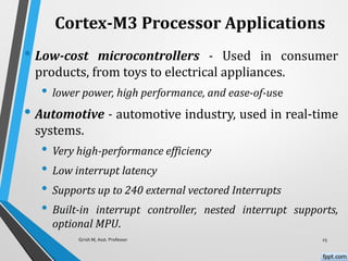
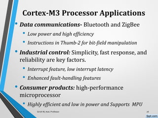
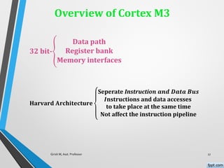
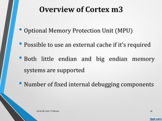
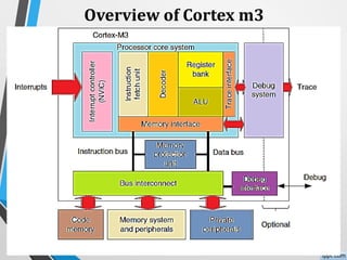
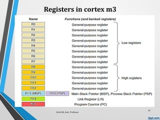
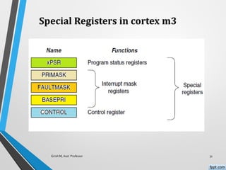
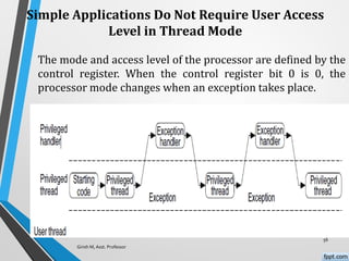
The document outlines the syllabus and key concepts related to ARM microcontrollers, specifically focusing on the ARM Cortex-M3 architecture. It discusses the advantages of ARM processors, including low power consumption, high performance, and ease of use, while highlighting the evolution and versatility of ARM technology in embedded systems. Additionally, the document details instruction sets, processor registers, and application areas for Cortex-M3, emphasizing its application in low-cost microcontrollers across various industries.