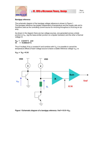
SlideShare a Scribd company logo
1 of 16
Download to read offline
Sheet
1 of 16
Bandgap reference
The schematic diagram of the bandgap voltage reference is shown in Figure 1.
The bandgap reference has largely independent of temperature and the supply rails and is
therefore used as the controlling current source for mirroring throughout a circuit eg an op-
amp.
As shown in the diagram there are two voltage sources, one generated across a diode
junction ie VBE (eg the base-emitter junction on a bipolar transistor) and the other a thermal
voltage Vt.
VBE = -2.2mV/˚C and
Vt = +0.085mV/˚C
Thus if multiply Vt by a constant K and combine with VBE it is possible to cancel the
temperature effects of each voltage source to leave a stable reference voltage VREF ie
VREF = VBE + K.Vt
VDD
VBE
VDD
Vt
K
Sum
Vref
K.Vt
Figure 1 Schematic diagram of a bandgap reference. Vref = K.Vt +VBE.
Sheet
2 of 16
Vbe
BJT_NPN
BJT2
Temp=Tc
Area=8
Model=BJTM1
VAR
VAR1
Tc=23
Eqn
Var
BJT_Model
BJTM1
Vje=0.7
NPN=yes
DC
DC1
Step=1
Stop=155
Start=-55
SweepVar="Tc"
DC
I_DC
SRC1
Idc=100 uA
Figure 2 ADS simulation setup to determine the temperature dependence of Vbe. The
temperature variable of the BJT model Tc is sweep by the DC simulation from –55 to
155 degrees C.
m1
Tc=-55.000
Vbe=795.6mV
m2
Tc=155.000
Vbe=418.3mV
m1
Tc=-55.000
Vbe=795.6mV
m2
Tc=155.000
Vbe=418.3mV
-40 -20 0 20 40 60 80 100 120 140-60 160
500
600
700
400
800
Tc
Vbe, mV
m1
m2
Eqn Tcoeff=1E3*(Vbe[210]-Vbe[0])/(Tc[210]-Tc[0])
Tcoeff
-1.7966 in mV
Figure 3 Temperature dependance of Vbe as simulated from the ADS simulation of
Figure 2. Temperature coefficient of VBE ~ -1.79mV/˚C.
Sheet
3 of 16
Temperature dependance of VBE
We can simulate the temperature effect of VBE by using the ADS simulation shown in Figure
2. In this simulation the temperature parameter of the generic spice BJT model (TC) is sweep
by the DC simulation from –55 to 155 degrees C.
The resulting plot of Vbe vs temperature is shown in Figure 3. An equation has been added to
calculate the temperature coefficient by taking the first and last data points [0] and [210] to
calculate the slope of the graph.
siliconfor1.12eVvoltagebandgapEgWhere(3)-
K.T
Eg-
.expTn
(2)-
2
3
-mWhere.Tµµ
variableskeyofdependanceeTemperatur
carriersminorityofMobilityµ
)cm(1.5x10SiliconinionconcentratcarrierIntrinsicn
Where
(1)-µ.K.T.nI
1-J.K10x1.3807constantBoltzmannsK
C10x1.602electrononchargeq
q
kT
Vtby WheregivenVoltageThermalVt
Where
Vt
V
.expIIc
-:bygiveniscurrentcollectorBipolar
32
i
m
O
3-102
i
2
iS
23-
19-
BE
s
==⎥
⎦
⎤
⎢
⎣
⎡
∝
≈∝
=
=
∝
==
==
==
=
⎟⎟
⎟
⎟
⎠
⎞
⎜⎜
⎜
⎜
⎝
⎛
Sheet
4 of 16
T
Is
.
I
V
Is
Ic
.Ln
T
V
T
V
x
y
x
1
Ln.axAs
T
Is
.
I
1
.V-
T
Is
Ln.IV-Ln.IcVgettooutexpand
T
Is
findTo
Is
Ic
.Ln
T
V
Is
Ic
.LnVof
T
V
Is
Ic
.LnVV
.KµincludesAconstantWhere
K.T
Eg-
.expA.T
K.T
Eg-
.exp.K.T.T.TµI
1into2&3equationsSub
S
TTBE
S
TSTT
T
T
BE
TBE
O
m43m
OS
∂
∂
−⎟
⎠
⎞
⎜
⎝
⎛
∂
∂
=
∂
∂
∂
∂
=
∂
∂
⇒
∂
∂
∴
∂
∂
⎟
⎠
⎞
⎜
⎝
⎛
∂
∂
⎟
⎠
⎞
⎜
⎝
⎛
∂
∂
⎟
⎠
⎞
⎜
⎝
⎛
=
⎥
⎦
⎤
⎢
⎣
⎡
=⎥
⎦
⎤
⎢
⎣
⎡
∝ +
( )
( )
( )
⎥
⎦
⎤
⎢
⎣
⎡
+
+
=
∂
∂
⎥
⎦
⎤
⎢
⎣
⎡+
⎥
⎦
⎤
⎢
⎣
⎡
⎥
⎦
⎤
⎢
⎣
⎡+
+
⎥
⎦
⎤
⎢
⎣
⎡+
⎥
⎦
⎤
⎢
⎣
⎡++
=
∂
∂
⎥
⎦
⎤
⎢
⎣
⎡
⎥
⎦
⎤
⎢
⎣
⎡++⎥
⎦
⎤
⎢
⎣
⎡++=
∂
∂
−=⎥
⎦
⎤
⎢
⎣
⎡+=
2T
T
S
T
2TT
S
T
2
n
S
K.T
Eg-
V
T
m4V
T
Is
.
I
V
K.T
Eg-
.expm4A.T
K.T
Eg-
.
K.T
Eg-
.expm4A.TV
K.T
Eg-
.expm4A.T
K.T
Eg-
.expm3A.Tm4V
T
Is
.
I
V
K.T
Eg-
.
K.T
Eg-
.expm4A.T
K.T
Eg-
.expm3A..Tm4
T
Is
dx
dy
.1nanxaxUse
K.T
Eg-
.expm4A.TI
Sheet
5 of 16
( )
( ) ( )
⎥
⎦
⎤
⎢
⎣
⎡
+
+
+
T
Eg-
q
1
T
m4V
T
V TBE
=⎥
⎦
⎤
⎢
⎣
⎡
+
+
+=
∂
∂
=⎟
⎠
⎞
⎜
⎝
⎛
=⎥
⎦
⎤
⎢
⎣
⎡
+
+
+⎟
⎠
⎞
⎜
⎝
⎛
=
∂
∂
−⎟
⎠
⎞
⎜
⎝
⎛
∂
∂
=
∂
∂
K.T
Eg-
q
kT
T
m4V
T
V
T
V
q
kT
Vt&
Is
Ic
.LnVV
K.T
Eg-
V
T
m4V
Is
Ic
.Ln
T
V
T
Is
.
I
V
Is
Ic
.Ln
T
V
T
V
2
TBEBE
TBE2T
TT
S
TTBE
Evaluation of dVBE/dT
area.Emitter-BaseA
)cm(1.5x10SiliconinionconcentratcarrierIntrinsicn
).s13cm(Typically
base.theinconstantdiffusionelectrontheforvalueeffectiveaverageTheDn
width.baseWdevice);type-pfor3x10NAprocess0.8um(for
emitter.theofareaunitperbasetheinatomsdopingofnumbertheis.NWQB
Where
A10to10arevaluesTypical
Q
Dn.q.A.n
IWhere
I
I
Vt.LnV
C10x1.602electrononchargeq
1-J.K10x1.3807constantBoltzmannsK
and
2
3
-m&1.12eV)silicon(forvoltageBandgapEqWhere
25.8mV
10x1.602
300.10x1.3807
q
KT
V
3-102
i
1-2
B
16
AB
16-14-
B
2
i
S
S
E
BE
19-
23-
19-
-23
T
=
=
=
=
==
=
=⎟⎟
⎠
⎞
⎜⎜
⎝
⎛
=
==
==
===
===
Sheet
6 of 16
( )
0.743V
1.562x10
50x10
.Ln108.52V
A1.562x10
3x10
.0.0131.5x10..1x101.602x10
Is
3x10.3x101x10.NWQ
Q
Dn.q.A.n
IWhere
I
I
Vt.LnV
then
1umA50uA,IEassumeVbeandVbeforvaluetypicalafindTo
17-
6-
3
BE
17-
10
2106-19-
10166-
ABB
B
2
i
S
S
E
BE
2
=⎟⎟
⎠
⎞
⎜⎜
⎝
⎛
=
=≈
===
=⎟⎟
⎠
⎞
⎜⎜
⎝
⎛
=
==∆
−
x
( )
K1.44mV/-
300
11.1108.52
2
3
-4-0.743
T
V
2
3
-m&1.12eV)silicon(forvoltageBandgapEqWhere
0.743VVBE&25.8mVV
T
q
Eq
Vm4-V
T
V
3
BE
T
TBE
BE
o
=
−⎟
⎠
⎞
⎜
⎝
⎛
=
∂
∂
===
==
−+
=
∂
∂
−
x
Sheet
7 of 16
VPTAT generation
The PTAT term is realised by determining the voltage difference between two forward-biased
diodes (eg VBE). MOS transistors operating in the weak inversion region can also be used to
form the diodes.
VBE
VDD
VR
Area = nA
Area = A
V01
V02
R
Q1
Q2
Figure 4 Generation of VPTAT voltage.
We can simulate the variation VPTAT over temperature using the ADS simulation shown in
Figure 5.
If we run the same simulation again but this time on the results graph we calculate Vref given
that we know vbe1 and (vbe1-vbe2). Various values of K were tried until the temperature
compensation was achieved as shown in the graph of Figure 7. This now forms the basis of
the band-gap reference in a practical circuit the voltage summing and setting of K is achieved
using a resistive network and an op-amp.
Sheet
8 of 16
Vbe1 Vbe2
BJT_NPN
BJT3
Temp=Tc
Area=2
Model=BJTM1R
R1
R=1 kOhmDC
DC1
Step=1
Stop=155
Start=-55
SweepVar="Tc"
DC
BJT_Model
BJTM1
Vje=0.7
NPN=yes
VAR
VAR1
Tc=23
Eqn
Var
BJT_NPN
BJT2
Temp=Tc
Area=1
Model=BJTM1
I_DC
SRC2
Idc=100 uA
I_DC
SRC1
Idc=100 uA
Figure 5 ADS simulation setup to analyse the variation of VPTAT over temperature. As
for the previous examples the temperature is swept in the DC simulation box. The
resulting plot is shown in Figure 6.
Sheet
9 of 16
EqnVTAT=Vbe1-Vbe2
m1
Tc=155.000
VTAT=0.026
m2
Tc=-55.000
VTAT=0.013
-40 -20 0 20 40 60 80 100 120 140-60 160
0.014
0.016
0.018
0.020
0.022
0.024
0.012
0.026
Tc
VTAT
m1
m2
Eqn VTAT_Temp=1e3*(VTAT[210]-VTAT[0])/(Tc[210]-Tc[0])
VTAT_Temp
0.060 mV
Figure 6 Resulting simulation of VPTAT vs temperature after running the simulation
shown in Figure 5.
.
Sheet
10 of 16
Figure 4 shows how the VPTAT voltage can be realised. If we force V01 and V02 to be the
same then the voltage across the resistor R will be the difference of the two VBE’s.
E2E1
2
1
2
1
E1
E2vt
VBE2-VBE1
vt
VBE2-VBE1
S1
S2
E1
E2
E2E1
E
kT
q.VBE
S
kT
q.VBE
SE
IIIf
A
A
A
A
I
I
e
thendeviceeachforsamethearevtandJsthatsuch
process,samethefromarestransistorAssume
q
kT
vtWheree
.JA
.JA
I
I
thenIIthatsuchconfigurediscircuitAssume
0IWheneA.J1eA.JI
=⎟⎟
⎠
⎞
⎜⎜
⎝
⎛
=⎟⎟
⎠
⎞
⎜⎜
⎝
⎛
⎟⎟
⎠
⎞
⎜⎜
⎝
⎛
=
=⎟⎟
⎠
⎞
⎜⎜
⎝
⎛
=
=
>
⎟
⎟
⎠
⎞
⎜
⎜
⎝
⎛
≈
⎟
⎟
⎠
⎞
⎜
⎜
⎝
⎛
−=
⎟⎟
⎠
⎞
⎜⎜
⎝
⎛
=⎟⎟
⎠
⎞
⎜⎜
⎝
⎛
=
2
1
2
1vt
VBE2-VBE1
A
A
vt.LnVBE2-VBE1givetoRearrange
A
A
e
( ) ( )
dx
dy
.1nanxaxUsingn.Ln
q
K
T
Vbe
n.Ln
q
KT
Vbe
q
KT
Vand
A
A
nLet
)I(I.R1IVbe
A
A
Vt.LnVBE1-VBE2thenAAIf
n
T
2
1
E2E1E1
2
1
21
−==
∂
∆∂
∴=∆∴
=⎟⎟
⎠
⎞
⎜⎜
⎝
⎛
=
==∆=⎟⎟
⎠
⎞
⎜⎜
⎝
⎛
=>
Where
K = Boltzmanns constant = 1.3807 x 10⁻²³
J.K-1
q = charge on electron = 1.602 x 10⁻¹⁹
C
A = Area of base-emitter junction um2
Sheet
11 of 16
EqnVTAT=Vbe1-Vbe2
EqnVref=Vbe1+(K*VTAT)
EqnK=27
-40 -20 0 20 40 60 80 100 120 140-60 160
1.186
1.187
1.188
1.189
1.190
1.185
1.191
Tc
Vref
Figure 7 Graph of the simulation shown in Figure 5. In this case we have calculated
VTAT ie vbe1-vbe2 and evaluated Vref from Vbe1+(K*VPTAT), where K = 27.
BandGap reference voltage
( ) K1.44mV/-
T
Eg-
q
1
T
m4V
T
V
T
V
J
J
Ln
T
V
T
∆Vbe
thereforeand
A
A
Ln
q
KT
J
J
Ln
q
KT
V-VVbefoundwePreviously
TBEBE
C2
C1T
2
1
C2
C1
BE2BE1
o
=⎥
⎦
⎤
⎢
⎣
⎡
+
+
+=
∂
∂
⎟⎟
⎠
⎞
⎜⎜
⎝
⎛
=
∂
∂
⎟⎟
⎠
⎞
⎜⎜
⎝
⎛
=⎟⎟
⎠
⎞
⎜⎜
⎝
⎛
==∆
Sheet
12 of 16
The band-gap reference voltage is given by:-
VREF = VBE + K.Vt
The temperature stable value of VREF at 300˚K is 1.262V. Therefore the value of K required is:
20.11
25.8x10
743.0262.1
K
25.8mV
10x1.602
300.10x1.3807
q
KT
V
earlier)d(Calculate0.743VWith
V
VV
K
KgettoRearrangeK.VVV
3-
19-
23-
T
BE
T
BEREF
TBEREF
=
−
=
===
=
−
=
+=
With reference to Figure 8.
The cascode current mirror makes I1 = I2 = I3
( )
( )
( )
( ) BE3OUT
BE3OUT
BE3OUT
2
1
2
1
BE1BE2
V.KNVt.LnV
V.K.RN.Ln
R
Vt
V
N.Ln
R
Vt
I3insubI2I3AsV.K.RI3V
I3I1N.Ln
R
Vt
I2soand
A
A
NLet
A
A
Vt.LnV-VVbeRacrossvoltageThe
+=∴
+=
==+=
===
=⎟⎟
⎠
⎞
⎜⎜
⎝
⎛
==∆=
Sheet
13 of 16
( )
Ω=∴
===∴
=
=⎟
⎠
⎞
⎜
⎝
⎛
=⎟
⎠
⎞
⎜
⎝
⎛
=
=
⎟
⎠
⎞
⎜
⎝
⎛
=
⎟
⎠
⎞
⎜
⎝
⎛
=
∆
=
=
+
==
=Ω=
−
10.45KK.R
10.45
)0.025.Ln(8
0.63-1.262
.Ln(N)V
Vbe-V
K
1.262VC23atvoltagereferencetcoefficienetemperaturzeroThe
0.0536V
1
8
(0.025).Ln
A2
A1
Vt.Ln∆ ∆VWith
C23at52uA
1x10
1
8
(0.025).Ln
R1
A2
A1
Vt.Ln
R1
Vbe
I
0.025V
10602.1
)23273.1.38x10
q
KT
vt
8N;1KRthatandC23ofetemperaturaAssume
T
REF
32
19
23-
o
o
o
x
Sheet
14 of 16
X.N
Vt
Vref
X
R
IE1
X.N
K.R
IE2
VEE
VDD
M1 M2
M3 M4
M5 M6
M7 M8
M10
M9
Q3
Q1
Q2
Figure 8 Circuit of the bandgap reference used in the example.
Sheet
15 of 16
The Bandgap circuit of Figure 8 was entered as a schematic into ADS as shown in figure and
analysed using a DC simulation block. For the simulation, the Temperature variable was
added to the active devices and resistor and the resistor initially set to 10K was varied until
the correct compensated curve resulted.
vout
vbe
R
R7
Temp=T
R=9 kOhm
VAR
VAR1
W=1.0
VDD=7.5
T=23
L=1.0
Eqn
Var LEVEL1_Model
MOSFETM2
Tox=24.7e-4
Mjsw=0.35
Cjsw=350e-12
Mj=0.5
Cj=560e-12
Cgbo=700E-12
Cgdo=220e-12
Cgso=220e-12
Lambda=0.04
Phi=0.8
Gamma=0.57
Kp=50e-6
Vto=-0.7
PMOS=yes
LEVEL1_Model
MOSFETM1
Tox=24.7e-4
Mjsw=0.38
Cjsw=380e-12
Mj=0.5
Cj=770e-12
Cgbo=700E-12
Cgdo=220e-12
Cgso=220e-12
Lambda=0.04
Phi=0.7
Gamma=0.4
Kp=110e-6
Vto=0.7
NMOS=yes
BJT_PNP
BJT1
Mode=nonlinear
Trise=
Temp=T
Region=
Area=10
Model=BJTM1
BJT_PNP
BJT3
Mode=nonlinear
Trise=
Temp=T
Region=
Area=10
Model=BJTM1
DC
DC1
Step=1
Stop=125
Start=-50
SweepVar="T"
DC
MOSFET_PMOS
MOSFET9
Temp=T
Width=2.2*W um
Length=L um
Model=MOSFETM2
MOSFET_NMOS
MOSFET1
Temp=T
Width=W um
Length=L um
Model=MOSFETM1
MOSFET_NMOS
MOSFET3
Temp=T
Width=W um
Length=L um
Model=MOSFETM1
MOSFET_NMOS
MOSFET6
Temp=T
Width=W um
Length=L um
Model=MOSFETM1
MOSFET_NMOS
MOSFET5
Temp=T
Width=W um
Length=L um
Model=MOSFETM1
MOSFET_PMOS
MOSFET7
Temp=T
Width=2.2*W um
Length=L um
Model=MOSFETM2
MOSFET_PMOS
MOSFET4
Temp=T
Width=2.2*W um
Length=L um
Model=MOSFETM2
MOSFET_PMOS
MOSFET8
Temp=T
Width=2.2*W um
Length=L um
Model=MOSFETM2
MOSFET_PMOS
MOSFET2
Temp=T
Width=2.2*W um
Length=L um
Model=MOSFETM2
MOSFET_PMOS
MOSFET10
Temp=T
Width=2.2*W um
Length=L um
Model=MOSFETM2
BJT_PNP
BJT2
Mode=nonlinear
Trise=
Temp=T
Region=
Area=1
Model=BJTM1
BJT_Model
BJTM1
Vje=0.7
NPN=no
R
R6
R=1 kOhm
V_DC
VDD
Vdc=VDD
Figure 9 ADS schematic setup for analysing the bandgap example circuit. R7 was
initially set to 10K (as per the hand calculations) and then varied to optimise the
bandgap voltage vs temperature curve shown in Figure 10
Sheet
16 of 16
-40 -20 0 20 40 60 80 100 120-60 140
1.164
1.166
1.168
1.162
1.170
T
vout, V
Figure 10 Resulting plot from the simulation shown in Figure 8. For this simulation the
temperature parameter for the active devices and resistor was varied over the
temperature range –50 to 125 deg C using the parameter sweep within the DC
simulation block.
One disadvantage of the example circuit is the headroom required on the supply rails. This is
because there are 4 VSAT+VT and a Vbe, resulting in the need to raise the supply from the
nominal +5V to +7.5V. Lower rail circuits tend to use low supply differential op-amp circuits.

More Related Content

What's hot

Easy labs exp4-beta meter
Easy labs exp4-beta meterEasy labs exp4-beta meter
Easy labs exp4-beta metermrinal mahato
 
Lab 7 Report Voltage Comparators and Schmitt Triggers
Lab 7 Report Voltage Comparators and Schmitt TriggersLab 7 Report Voltage Comparators and Schmitt Triggers
Lab 7 Report Voltage Comparators and Schmitt TriggersKatrina Little
 
Basic electronics Tutorial 3
Basic electronics Tutorial 3Basic electronics Tutorial 3
Basic electronics Tutorial 3Ankit Kumar
 
Basic electronics Tutorial 2
Basic electronics Tutorial 2Basic electronics Tutorial 2
Basic electronics Tutorial 2Ankit Kumar
 
Transformador excercises para compartir
Transformador excercises para compartirTransformador excercises para compartir
Transformador excercises para compartirJehAlvitezVzquez
 
Transistor bias circuit
Transistor bias circuitTransistor bias circuit
Transistor bias circuitAdk Adool
 
analisa sistem tenaga lanjut
analisa sistem tenaga lanjutanalisa sistem tenaga lanjut
analisa sistem tenaga lanjutsuparman unkhair
 
Jawaban uts astl ganjil analisa sistem tenaga
Jawaban uts astl ganjil analisa sistem tenagaJawaban uts astl ganjil analisa sistem tenaga
Jawaban uts astl ganjil analisa sistem tenagasuparman unkhair
 
Small signal analysis of bjt amplifiers
Small signal analysis of bjt amplifiersSmall signal analysis of bjt amplifiers
Small signal analysis of bjt amplifiersPRAVEENA N G
 
3 phase diode bridge rectifier
3 phase diode bridge rectifier3 phase diode bridge rectifier
3 phase diode bridge rectifierMihir Taylor
 
Solucionario serway cap 27
Solucionario serway cap 27Solucionario serway cap 27
Solucionario serway cap 27Carlo Magno
 
Eet3082 binod kumar sahu lecturer_14
Eet3082 binod kumar sahu lecturer_14Eet3082 binod kumar sahu lecturer_14
Eet3082 binod kumar sahu lecturer_14BinodKumarSahu5
 
Optimized, Low-Power Dissipative and Precise Pulsating Constant Current Sourc...
Optimized, Low-Power Dissipative and Precise Pulsating Constant Current Sourc...Optimized, Low-Power Dissipative and Precise Pulsating Constant Current Sourc...
Optimized, Low-Power Dissipative and Precise Pulsating Constant Current Sourc...IJMER
 
Fuentes de voltajes continuas k j c (1)
Fuentes de voltajes continuas k j c (1)Fuentes de voltajes continuas k j c (1)
Fuentes de voltajes continuas k j c (1)vandreadelmorales
 
EE201 -Chapter 4
EE201 -Chapter 4 EE201 -Chapter 4
EE201 -Chapter 4 ruhiyah
 

What's hot (19)

Easy labs exp4-beta meter
Easy labs exp4-beta meterEasy labs exp4-beta meter
Easy labs exp4-beta meter
 
Lab 7 Report Voltage Comparators and Schmitt Triggers
Lab 7 Report Voltage Comparators and Schmitt TriggersLab 7 Report Voltage Comparators and Schmitt Triggers
Lab 7 Report Voltage Comparators and Schmitt Triggers
 
Basic electronics Tutorial 3
Basic electronics Tutorial 3Basic electronics Tutorial 3
Basic electronics Tutorial 3
 
Calor especifico del agua
Calor especifico del aguaCalor especifico del agua
Calor especifico del agua
 
Capacitance jee assignment
Capacitance jee assignmentCapacitance jee assignment
Capacitance jee assignment
 
Basic electronics Tutorial 2
Basic electronics Tutorial 2Basic electronics Tutorial 2
Basic electronics Tutorial 2
 
Transformador excercises para compartir
Transformador excercises para compartirTransformador excercises para compartir
Transformador excercises para compartir
 
Transistor bias circuit
Transistor bias circuitTransistor bias circuit
Transistor bias circuit
 
analisa sistem tenaga lanjut
analisa sistem tenaga lanjutanalisa sistem tenaga lanjut
analisa sistem tenaga lanjut
 
Dtc (1)
Dtc (1)Dtc (1)
Dtc (1)
 
Jawaban uts astl ganjil analisa sistem tenaga
Jawaban uts astl ganjil analisa sistem tenagaJawaban uts astl ganjil analisa sistem tenaga
Jawaban uts astl ganjil analisa sistem tenaga
 
Small signal analysis of bjt amplifiers
Small signal analysis of bjt amplifiersSmall signal analysis of bjt amplifiers
Small signal analysis of bjt amplifiers
 
3 phase diode bridge rectifier
3 phase diode bridge rectifier3 phase diode bridge rectifier
3 phase diode bridge rectifier
 
Solucionario serway cap 27
Solucionario serway cap 27Solucionario serway cap 27
Solucionario serway cap 27
 
Eet3082 binod kumar sahu lecturer_14
Eet3082 binod kumar sahu lecturer_14Eet3082 binod kumar sahu lecturer_14
Eet3082 binod kumar sahu lecturer_14
 
Optimized, Low-Power Dissipative and Precise Pulsating Constant Current Sourc...
Optimized, Low-Power Dissipative and Precise Pulsating Constant Current Sourc...Optimized, Low-Power Dissipative and Precise Pulsating Constant Current Sourc...
Optimized, Low-Power Dissipative and Precise Pulsating Constant Current Sourc...
 
Fuentes de voltajes continuas k j c (1)
Fuentes de voltajes continuas k j c (1)Fuentes de voltajes continuas k j c (1)
Fuentes de voltajes continuas k j c (1)
 
Unit 2
Unit 2Unit 2
Unit 2
 
EE201 -Chapter 4
EE201 -Chapter 4 EE201 -Chapter 4
EE201 -Chapter 4
 

Similar to Aaaa jjjjjjjj band gap pdf

Lect2 up170 (100420)
Lect2 up170 (100420)Lect2 up170 (100420)
Lect2 up170 (100420)aicdesign
 
IC Design of Power Management Circuits (IV)
IC Design of Power Management Circuits (IV)IC Design of Power Management Circuits (IV)
IC Design of Power Management Circuits (IV)Claudia Sin
 
lecture17-180515 for cmos analog circuit design.pdf
lecture17-180515 for cmos analog circuit design.pdflecture17-180515 for cmos analog circuit design.pdf
lecture17-180515 for cmos analog circuit design.pdfajmunesyar
 
Intro electronics laboratory
Intro electronics laboratoryIntro electronics laboratory
Intro electronics laboratoryThinh Pham Quoc
 
Multisim_simulation_project_3_^0_4[1]-2.pptx
Multisim_simulation_project_3_^0_4[1]-2.pptxMultisim_simulation_project_3_^0_4[1]-2.pptx
Multisim_simulation_project_3_^0_4[1]-2.pptxwencove9
 
SERIES RESISTOR-CAPASITOR CIRCUIT experiment 7
SERIES RESISTOR-CAPASITOR CIRCUIT experiment 7SERIES RESISTOR-CAPASITOR CIRCUIT experiment 7
SERIES RESISTOR-CAPASITOR CIRCUIT experiment 7Karimi LordRamza
 
Ee6378 bandgap reference
Ee6378 bandgap referenceEe6378 bandgap reference
Ee6378 bandgap referencessuser2038c9
 
L 09(gdr)(et) ((ee)nptel)
L 09(gdr)(et) ((ee)nptel)L 09(gdr)(et) ((ee)nptel)
L 09(gdr)(et) ((ee)nptel)Pradeep Godara
 
node analysis.pptx
node analysis.pptxnode analysis.pptx
node analysis.pptxARCHISTUDIO1
 
Optimization of Temperature Coefficient and Noise Analysis of MOSFET- Only Vo...
Optimization of Temperature Coefficient and Noise Analysis of MOSFET- Only Vo...Optimization of Temperature Coefficient and Noise Analysis of MOSFET- Only Vo...
Optimization of Temperature Coefficient and Noise Analysis of MOSFET- Only Vo...IJERA Editor
 
Space vector pwm_inverter
Space vector pwm_inverterSpace vector pwm_inverter
Space vector pwm_inverterZunAib Ali
 
Electric Circuits Lab Series RC Circuits Phase Angle, Phase Lag.docx
Electric Circuits Lab Series RC Circuits Phase Angle, Phase Lag.docxElectric Circuits Lab Series RC Circuits Phase Angle, Phase Lag.docx
Electric Circuits Lab Series RC Circuits Phase Angle, Phase Lag.docxpauline234567
 
2426Lab7Series&ParallelCircuits
2426Lab7Series&ParallelCircuits2426Lab7Series&ParallelCircuits
2426Lab7Series&ParallelCircuitsTaylor Huston
 
Ee6378 linear regulators
Ee6378 linear regulatorsEe6378 linear regulators
Ee6378 linear regulatorsssuser2038c9
 

Similar to Aaaa jjjjjjjj band gap pdf (20)

Lect2 up170 (100420)
Lect2 up170 (100420)Lect2 up170 (100420)
Lect2 up170 (100420)
 
IC Design of Power Management Circuits (IV)
IC Design of Power Management Circuits (IV)IC Design of Power Management Circuits (IV)
IC Design of Power Management Circuits (IV)
 
lecture17-180515 for cmos analog circuit design.pdf
lecture17-180515 for cmos analog circuit design.pdflecture17-180515 for cmos analog circuit design.pdf
lecture17-180515 for cmos analog circuit design.pdf
 
Intro electronics laboratory
Intro electronics laboratoryIntro electronics laboratory
Intro electronics laboratory
 
Multisim_simulation_project_3_^0_4[1]-2.pptx
Multisim_simulation_project_3_^0_4[1]-2.pptxMultisim_simulation_project_3_^0_4[1]-2.pptx
Multisim_simulation_project_3_^0_4[1]-2.pptx
 
SERIES RESISTOR-CAPASITOR CIRCUIT experiment 7
SERIES RESISTOR-CAPASITOR CIRCUIT experiment 7SERIES RESISTOR-CAPASITOR CIRCUIT experiment 7
SERIES RESISTOR-CAPASITOR CIRCUIT experiment 7
 
COBEP_2007
COBEP_2007COBEP_2007
COBEP_2007
 
Ee6378 bandgap reference
Ee6378 bandgap referenceEe6378 bandgap reference
Ee6378 bandgap reference
 
L 09(gdr)(et) ((ee)nptel)
L 09(gdr)(et) ((ee)nptel)L 09(gdr)(et) ((ee)nptel)
L 09(gdr)(et) ((ee)nptel)
 
Experimental Verification of Single Phase Z Source Inverter for Photovoltaic ...
Experimental Verification of Single Phase Z Source Inverter for Photovoltaic ...Experimental Verification of Single Phase Z Source Inverter for Photovoltaic ...
Experimental Verification of Single Phase Z Source Inverter for Photovoltaic ...
 
node analysis.pptx
node analysis.pptxnode analysis.pptx
node analysis.pptx
 
D05432435
D05432435D05432435
D05432435
 
Optimization of Temperature Coefficient and Noise Analysis of MOSFET- Only Vo...
Optimization of Temperature Coefficient and Noise Analysis of MOSFET- Only Vo...Optimization of Temperature Coefficient and Noise Analysis of MOSFET- Only Vo...
Optimization of Temperature Coefficient and Noise Analysis of MOSFET- Only Vo...
 
Assignmentl3 solutions
Assignmentl3 solutionsAssignmentl3 solutions
Assignmentl3 solutions
 
Space vector pwm_inverter
Space vector pwm_inverterSpace vector pwm_inverter
Space vector pwm_inverter
 
Electric Circuits Lab Series RC Circuits Phase Angle, Phase Lag.docx
Electric Circuits Lab Series RC Circuits Phase Angle, Phase Lag.docxElectric Circuits Lab Series RC Circuits Phase Angle, Phase Lag.docx
Electric Circuits Lab Series RC Circuits Phase Angle, Phase Lag.docx
 
module2.pdf
module2.pdfmodule2.pdf
module2.pdf
 
2426Lab7Series&ParallelCircuits
2426Lab7Series&ParallelCircuits2426Lab7Series&ParallelCircuits
2426Lab7Series&ParallelCircuits
 
Ee6378 linear regulators
Ee6378 linear regulatorsEe6378 linear regulators
Ee6378 linear regulators
 
99992505.pdf
99992505.pdf99992505.pdf
99992505.pdf
 

Recently uploaded

Recombination DNA Technology (Nucleic Acid Hybridization )
Recombination DNA Technology (Nucleic Acid Hybridization )Recombination DNA Technology (Nucleic Acid Hybridization )
Recombination DNA Technology (Nucleic Acid Hybridization )aarthirajkumar25
 
Recombinant DNA technology (Immunological screening)
Recombinant DNA technology (Immunological screening)Recombinant DNA technology (Immunological screening)
Recombinant DNA technology (Immunological screening)PraveenaKalaiselvan1
 
Nanoparticles synthesis and characterization​ ​
Nanoparticles synthesis and characterization​  ​Nanoparticles synthesis and characterization​  ​
Nanoparticles synthesis and characterization​ ​kaibalyasahoo82800
 
Kochi ❤CALL GIRL 84099*07087 ❤CALL GIRLS IN Kochi ESCORT SERVICE❤CALL GIRL
Kochi ❤CALL GIRL 84099*07087 ❤CALL GIRLS IN Kochi ESCORT SERVICE❤CALL GIRLKochi ❤CALL GIRL 84099*07087 ❤CALL GIRLS IN Kochi ESCORT SERVICE❤CALL GIRL
Kochi ❤CALL GIRL 84099*07087 ❤CALL GIRLS IN Kochi ESCORT SERVICE❤CALL GIRLkantirani197
 
Forensic Biology & Its biological significance.pdf
Forensic Biology & Its biological significance.pdfForensic Biology & Its biological significance.pdf
Forensic Biology & Its biological significance.pdfrohankumarsinghrore1
 
Pests of mustard_Identification_Management_Dr.UPR.pdf
Pests of mustard_Identification_Management_Dr.UPR.pdfPests of mustard_Identification_Management_Dr.UPR.pdf
Pests of mustard_Identification_Management_Dr.UPR.pdfPirithiRaju
 
Botany 4th semester series (krishna).pdf
Botany 4th semester series (krishna).pdfBotany 4th semester series (krishna).pdf
Botany 4th semester series (krishna).pdfSumit Kumar yadav
 
GUIDELINES ON SIMILAR BIOLOGICS Regulatory Requirements for Marketing Authori...
GUIDELINES ON SIMILAR BIOLOGICS Regulatory Requirements for Marketing Authori...GUIDELINES ON SIMILAR BIOLOGICS Regulatory Requirements for Marketing Authori...
GUIDELINES ON SIMILAR BIOLOGICS Regulatory Requirements for Marketing Authori...Lokesh Kothari
 
Zoology 4th semester series (krishna).pdf
Zoology 4th semester series (krishna).pdfZoology 4th semester series (krishna).pdf
Zoology 4th semester series (krishna).pdfSumit Kumar yadav
 
Hubble Asteroid Hunter III. Physical properties of newly found asteroids
Hubble Asteroid Hunter III. Physical properties of newly found asteroidsHubble Asteroid Hunter III. Physical properties of newly found asteroids
Hubble Asteroid Hunter III. Physical properties of newly found asteroidsSérgio Sacani
 
Isotopic evidence of long-lived volcanism on Io
Isotopic evidence of long-lived volcanism on IoIsotopic evidence of long-lived volcanism on Io
Isotopic evidence of long-lived volcanism on IoSérgio Sacani
 
Botany 4th semester file By Sumit Kumar yadav.pdf
Botany 4th semester file By Sumit Kumar yadav.pdfBotany 4th semester file By Sumit Kumar yadav.pdf
Botany 4th semester file By Sumit Kumar yadav.pdfSumit Kumar yadav
 
Green chemistry and Sustainable development.pptx
Green chemistry  and Sustainable development.pptxGreen chemistry  and Sustainable development.pptx
Green chemistry and Sustainable development.pptxRajatChauhan518211
 
Chemistry 4th semester series (krishna).pdf
Chemistry 4th semester series (krishna).pdfChemistry 4th semester series (krishna).pdf
Chemistry 4th semester series (krishna).pdfSumit Kumar yadav
 
GBSN - Microbiology (Unit 2)
GBSN - Microbiology (Unit 2)GBSN - Microbiology (Unit 2)
GBSN - Microbiology (Unit 2)Areesha Ahmad
 
Presentation Vikram Lander by Vedansh Gupta.pptx
Presentation Vikram Lander by Vedansh Gupta.pptxPresentation Vikram Lander by Vedansh Gupta.pptx
Presentation Vikram Lander by Vedansh Gupta.pptxgindu3009
 
GBSN - Biochemistry (Unit 1)
GBSN - Biochemistry (Unit 1)GBSN - Biochemistry (Unit 1)
GBSN - Biochemistry (Unit 1)Areesha Ahmad
 
PossibleEoarcheanRecordsoftheGeomagneticFieldPreservedintheIsuaSupracrustalBe...
PossibleEoarcheanRecordsoftheGeomagneticFieldPreservedintheIsuaSupracrustalBe...PossibleEoarcheanRecordsoftheGeomagneticFieldPreservedintheIsuaSupracrustalBe...
PossibleEoarcheanRecordsoftheGeomagneticFieldPreservedintheIsuaSupracrustalBe...Sérgio Sacani
 
Hire 💕 9907093804 Hooghly Call Girls Service Call Girls Agency
Hire 💕 9907093804 Hooghly Call Girls Service Call Girls AgencyHire 💕 9907093804 Hooghly Call Girls Service Call Girls Agency
Hire 💕 9907093804 Hooghly Call Girls Service Call Girls AgencySheetal Arora
 
Pests of cotton_Sucking_Pests_Dr.UPR.pdf
Pests of cotton_Sucking_Pests_Dr.UPR.pdfPests of cotton_Sucking_Pests_Dr.UPR.pdf
Pests of cotton_Sucking_Pests_Dr.UPR.pdfPirithiRaju
 

Recently uploaded (20)

Recombination DNA Technology (Nucleic Acid Hybridization )
Recombination DNA Technology (Nucleic Acid Hybridization )Recombination DNA Technology (Nucleic Acid Hybridization )
Recombination DNA Technology (Nucleic Acid Hybridization )
 
Recombinant DNA technology (Immunological screening)
Recombinant DNA technology (Immunological screening)Recombinant DNA technology (Immunological screening)
Recombinant DNA technology (Immunological screening)
 
Nanoparticles synthesis and characterization​ ​
Nanoparticles synthesis and characterization​  ​Nanoparticles synthesis and characterization​  ​
Nanoparticles synthesis and characterization​ ​
 
Kochi ❤CALL GIRL 84099*07087 ❤CALL GIRLS IN Kochi ESCORT SERVICE❤CALL GIRL
Kochi ❤CALL GIRL 84099*07087 ❤CALL GIRLS IN Kochi ESCORT SERVICE❤CALL GIRLKochi ❤CALL GIRL 84099*07087 ❤CALL GIRLS IN Kochi ESCORT SERVICE❤CALL GIRL
Kochi ❤CALL GIRL 84099*07087 ❤CALL GIRLS IN Kochi ESCORT SERVICE❤CALL GIRL
 
Forensic Biology & Its biological significance.pdf
Forensic Biology & Its biological significance.pdfForensic Biology & Its biological significance.pdf
Forensic Biology & Its biological significance.pdf
 
Pests of mustard_Identification_Management_Dr.UPR.pdf
Pests of mustard_Identification_Management_Dr.UPR.pdfPests of mustard_Identification_Management_Dr.UPR.pdf
Pests of mustard_Identification_Management_Dr.UPR.pdf
 
Botany 4th semester series (krishna).pdf
Botany 4th semester series (krishna).pdfBotany 4th semester series (krishna).pdf
Botany 4th semester series (krishna).pdf
 
GUIDELINES ON SIMILAR BIOLOGICS Regulatory Requirements for Marketing Authori...
GUIDELINES ON SIMILAR BIOLOGICS Regulatory Requirements for Marketing Authori...GUIDELINES ON SIMILAR BIOLOGICS Regulatory Requirements for Marketing Authori...
GUIDELINES ON SIMILAR BIOLOGICS Regulatory Requirements for Marketing Authori...
 
Zoology 4th semester series (krishna).pdf
Zoology 4th semester series (krishna).pdfZoology 4th semester series (krishna).pdf
Zoology 4th semester series (krishna).pdf
 
Hubble Asteroid Hunter III. Physical properties of newly found asteroids
Hubble Asteroid Hunter III. Physical properties of newly found asteroidsHubble Asteroid Hunter III. Physical properties of newly found asteroids
Hubble Asteroid Hunter III. Physical properties of newly found asteroids
 
Isotopic evidence of long-lived volcanism on Io
Isotopic evidence of long-lived volcanism on IoIsotopic evidence of long-lived volcanism on Io
Isotopic evidence of long-lived volcanism on Io
 
Botany 4th semester file By Sumit Kumar yadav.pdf
Botany 4th semester file By Sumit Kumar yadav.pdfBotany 4th semester file By Sumit Kumar yadav.pdf
Botany 4th semester file By Sumit Kumar yadav.pdf
 
Green chemistry and Sustainable development.pptx
Green chemistry  and Sustainable development.pptxGreen chemistry  and Sustainable development.pptx
Green chemistry and Sustainable development.pptx
 
Chemistry 4th semester series (krishna).pdf
Chemistry 4th semester series (krishna).pdfChemistry 4th semester series (krishna).pdf
Chemistry 4th semester series (krishna).pdf
 
GBSN - Microbiology (Unit 2)
GBSN - Microbiology (Unit 2)GBSN - Microbiology (Unit 2)
GBSN - Microbiology (Unit 2)
 
Presentation Vikram Lander by Vedansh Gupta.pptx
Presentation Vikram Lander by Vedansh Gupta.pptxPresentation Vikram Lander by Vedansh Gupta.pptx
Presentation Vikram Lander by Vedansh Gupta.pptx
 
GBSN - Biochemistry (Unit 1)
GBSN - Biochemistry (Unit 1)GBSN - Biochemistry (Unit 1)
GBSN - Biochemistry (Unit 1)
 
PossibleEoarcheanRecordsoftheGeomagneticFieldPreservedintheIsuaSupracrustalBe...
PossibleEoarcheanRecordsoftheGeomagneticFieldPreservedintheIsuaSupracrustalBe...PossibleEoarcheanRecordsoftheGeomagneticFieldPreservedintheIsuaSupracrustalBe...
PossibleEoarcheanRecordsoftheGeomagneticFieldPreservedintheIsuaSupracrustalBe...
 
Hire 💕 9907093804 Hooghly Call Girls Service Call Girls Agency
Hire 💕 9907093804 Hooghly Call Girls Service Call Girls AgencyHire 💕 9907093804 Hooghly Call Girls Service Call Girls Agency
Hire 💕 9907093804 Hooghly Call Girls Service Call Girls Agency
 
Pests of cotton_Sucking_Pests_Dr.UPR.pdf
Pests of cotton_Sucking_Pests_Dr.UPR.pdfPests of cotton_Sucking_Pests_Dr.UPR.pdf
Pests of cotton_Sucking_Pests_Dr.UPR.pdf
 

Aaaa jjjjjjjj band gap pdf

  • 1. Sheet 1 of 16 Bandgap reference The schematic diagram of the bandgap voltage reference is shown in Figure 1. The bandgap reference has largely independent of temperature and the supply rails and is therefore used as the controlling current source for mirroring throughout a circuit eg an op- amp. As shown in the diagram there are two voltage sources, one generated across a diode junction ie VBE (eg the base-emitter junction on a bipolar transistor) and the other a thermal voltage Vt. VBE = -2.2mV/˚C and Vt = +0.085mV/˚C Thus if multiply Vt by a constant K and combine with VBE it is possible to cancel the temperature effects of each voltage source to leave a stable reference voltage VREF ie VREF = VBE + K.Vt VDD VBE VDD Vt K Sum Vref K.Vt Figure 1 Schematic diagram of a bandgap reference. Vref = K.Vt +VBE.
  • 2. Sheet 2 of 16 Vbe BJT_NPN BJT2 Temp=Tc Area=8 Model=BJTM1 VAR VAR1 Tc=23 Eqn Var BJT_Model BJTM1 Vje=0.7 NPN=yes DC DC1 Step=1 Stop=155 Start=-55 SweepVar="Tc" DC I_DC SRC1 Idc=100 uA Figure 2 ADS simulation setup to determine the temperature dependence of Vbe. The temperature variable of the BJT model Tc is sweep by the DC simulation from –55 to 155 degrees C. m1 Tc=-55.000 Vbe=795.6mV m2 Tc=155.000 Vbe=418.3mV m1 Tc=-55.000 Vbe=795.6mV m2 Tc=155.000 Vbe=418.3mV -40 -20 0 20 40 60 80 100 120 140-60 160 500 600 700 400 800 Tc Vbe, mV m1 m2 Eqn Tcoeff=1E3*(Vbe[210]-Vbe[0])/(Tc[210]-Tc[0]) Tcoeff -1.7966 in mV Figure 3 Temperature dependance of Vbe as simulated from the ADS simulation of Figure 2. Temperature coefficient of VBE ~ -1.79mV/˚C.
  • 3. Sheet 3 of 16 Temperature dependance of VBE We can simulate the temperature effect of VBE by using the ADS simulation shown in Figure 2. In this simulation the temperature parameter of the generic spice BJT model (TC) is sweep by the DC simulation from –55 to 155 degrees C. The resulting plot of Vbe vs temperature is shown in Figure 3. An equation has been added to calculate the temperature coefficient by taking the first and last data points [0] and [210] to calculate the slope of the graph. siliconfor1.12eVvoltagebandgapEgWhere(3)- K.T Eg- .expTn (2)- 2 3 -mWhere.Tµµ variableskeyofdependanceeTemperatur carriersminorityofMobilityµ )cm(1.5x10SiliconinionconcentratcarrierIntrinsicn Where (1)-µ.K.T.nI 1-J.K10x1.3807constantBoltzmannsK C10x1.602electrononchargeq q kT Vtby WheregivenVoltageThermalVt Where Vt V .expIIc -:bygiveniscurrentcollectorBipolar 32 i m O 3-102 i 2 iS 23- 19- BE s ==⎥ ⎦ ⎤ ⎢ ⎣ ⎡ ∝ ≈∝ = = ∝ == == == = ⎟⎟ ⎟ ⎟ ⎠ ⎞ ⎜⎜ ⎜ ⎜ ⎝ ⎛
  • 4. Sheet 4 of 16 T Is . I V Is Ic .Ln T V T V x y x 1 Ln.axAs T Is . I 1 .V- T Is Ln.IV-Ln.IcVgettooutexpand T Is findTo Is Ic .Ln T V Is Ic .LnVof T V Is Ic .LnVV .KµincludesAconstantWhere K.T Eg- .expA.T K.T Eg- .exp.K.T.T.TµI 1into2&3equationsSub S TTBE S TSTT T T BE TBE O m43m OS ∂ ∂ −⎟ ⎠ ⎞ ⎜ ⎝ ⎛ ∂ ∂ = ∂ ∂ ∂ ∂ = ∂ ∂ ⇒ ∂ ∂ ∴ ∂ ∂ ⎟ ⎠ ⎞ ⎜ ⎝ ⎛ ∂ ∂ ⎟ ⎠ ⎞ ⎜ ⎝ ⎛ ∂ ∂ ⎟ ⎠ ⎞ ⎜ ⎝ ⎛ = ⎥ ⎦ ⎤ ⎢ ⎣ ⎡ =⎥ ⎦ ⎤ ⎢ ⎣ ⎡ ∝ + ( ) ( ) ( ) ⎥ ⎦ ⎤ ⎢ ⎣ ⎡ + + = ∂ ∂ ⎥ ⎦ ⎤ ⎢ ⎣ ⎡+ ⎥ ⎦ ⎤ ⎢ ⎣ ⎡ ⎥ ⎦ ⎤ ⎢ ⎣ ⎡+ + ⎥ ⎦ ⎤ ⎢ ⎣ ⎡+ ⎥ ⎦ ⎤ ⎢ ⎣ ⎡++ = ∂ ∂ ⎥ ⎦ ⎤ ⎢ ⎣ ⎡ ⎥ ⎦ ⎤ ⎢ ⎣ ⎡++⎥ ⎦ ⎤ ⎢ ⎣ ⎡++= ∂ ∂ −=⎥ ⎦ ⎤ ⎢ ⎣ ⎡+= 2T T S T 2TT S T 2 n S K.T Eg- V T m4V T Is . I V K.T Eg- .expm4A.T K.T Eg- . K.T Eg- .expm4A.TV K.T Eg- .expm4A.T K.T Eg- .expm3A.Tm4V T Is . I V K.T Eg- . K.T Eg- .expm4A.T K.T Eg- .expm3A..Tm4 T Is dx dy .1nanxaxUse K.T Eg- .expm4A.TI
  • 5. Sheet 5 of 16 ( ) ( ) ( ) ⎥ ⎦ ⎤ ⎢ ⎣ ⎡ + + + T Eg- q 1 T m4V T V TBE =⎥ ⎦ ⎤ ⎢ ⎣ ⎡ + + += ∂ ∂ =⎟ ⎠ ⎞ ⎜ ⎝ ⎛ =⎥ ⎦ ⎤ ⎢ ⎣ ⎡ + + +⎟ ⎠ ⎞ ⎜ ⎝ ⎛ = ∂ ∂ −⎟ ⎠ ⎞ ⎜ ⎝ ⎛ ∂ ∂ = ∂ ∂ K.T Eg- q kT T m4V T V T V q kT Vt& Is Ic .LnVV K.T Eg- V T m4V Is Ic .Ln T V T Is . I V Is Ic .Ln T V T V 2 TBEBE TBE2T TT S TTBE Evaluation of dVBE/dT area.Emitter-BaseA )cm(1.5x10SiliconinionconcentratcarrierIntrinsicn ).s13cm(Typically base.theinconstantdiffusionelectrontheforvalueeffectiveaverageTheDn width.baseWdevice);type-pfor3x10NAprocess0.8um(for emitter.theofareaunitperbasetheinatomsdopingofnumbertheis.NWQB Where A10to10arevaluesTypical Q Dn.q.A.n IWhere I I Vt.LnV C10x1.602electrononchargeq 1-J.K10x1.3807constantBoltzmannsK and 2 3 -m&1.12eV)silicon(forvoltageBandgapEqWhere 25.8mV 10x1.602 300.10x1.3807 q KT V 3-102 i 1-2 B 16 AB 16-14- B 2 i S S E BE 19- 23- 19- -23 T = = = = == = =⎟⎟ ⎠ ⎞ ⎜⎜ ⎝ ⎛ = == == === ===
  • 6. Sheet 6 of 16 ( ) 0.743V 1.562x10 50x10 .Ln108.52V A1.562x10 3x10 .0.0131.5x10..1x101.602x10 Is 3x10.3x101x10.NWQ Q Dn.q.A.n IWhere I I Vt.LnV then 1umA50uA,IEassumeVbeandVbeforvaluetypicalafindTo 17- 6- 3 BE 17- 10 2106-19- 10166- ABB B 2 i S S E BE 2 =⎟⎟ ⎠ ⎞ ⎜⎜ ⎝ ⎛ = =≈ === =⎟⎟ ⎠ ⎞ ⎜⎜ ⎝ ⎛ = ==∆ − x ( ) K1.44mV/- 300 11.1108.52 2 3 -4-0.743 T V 2 3 -m&1.12eV)silicon(forvoltageBandgapEqWhere 0.743VVBE&25.8mVV T q Eq Vm4-V T V 3 BE T TBE BE o = −⎟ ⎠ ⎞ ⎜ ⎝ ⎛ = ∂ ∂ === == −+ = ∂ ∂ − x
  • 7. Sheet 7 of 16 VPTAT generation The PTAT term is realised by determining the voltage difference between two forward-biased diodes (eg VBE). MOS transistors operating in the weak inversion region can also be used to form the diodes. VBE VDD VR Area = nA Area = A V01 V02 R Q1 Q2 Figure 4 Generation of VPTAT voltage. We can simulate the variation VPTAT over temperature using the ADS simulation shown in Figure 5. If we run the same simulation again but this time on the results graph we calculate Vref given that we know vbe1 and (vbe1-vbe2). Various values of K were tried until the temperature compensation was achieved as shown in the graph of Figure 7. This now forms the basis of the band-gap reference in a practical circuit the voltage summing and setting of K is achieved using a resistive network and an op-amp.
  • 8. Sheet 8 of 16 Vbe1 Vbe2 BJT_NPN BJT3 Temp=Tc Area=2 Model=BJTM1R R1 R=1 kOhmDC DC1 Step=1 Stop=155 Start=-55 SweepVar="Tc" DC BJT_Model BJTM1 Vje=0.7 NPN=yes VAR VAR1 Tc=23 Eqn Var BJT_NPN BJT2 Temp=Tc Area=1 Model=BJTM1 I_DC SRC2 Idc=100 uA I_DC SRC1 Idc=100 uA Figure 5 ADS simulation setup to analyse the variation of VPTAT over temperature. As for the previous examples the temperature is swept in the DC simulation box. The resulting plot is shown in Figure 6.
  • 9. Sheet 9 of 16 EqnVTAT=Vbe1-Vbe2 m1 Tc=155.000 VTAT=0.026 m2 Tc=-55.000 VTAT=0.013 -40 -20 0 20 40 60 80 100 120 140-60 160 0.014 0.016 0.018 0.020 0.022 0.024 0.012 0.026 Tc VTAT m1 m2 Eqn VTAT_Temp=1e3*(VTAT[210]-VTAT[0])/(Tc[210]-Tc[0]) VTAT_Temp 0.060 mV Figure 6 Resulting simulation of VPTAT vs temperature after running the simulation shown in Figure 5. .
  • 10. Sheet 10 of 16 Figure 4 shows how the VPTAT voltage can be realised. If we force V01 and V02 to be the same then the voltage across the resistor R will be the difference of the two VBE’s. E2E1 2 1 2 1 E1 E2vt VBE2-VBE1 vt VBE2-VBE1 S1 S2 E1 E2 E2E1 E kT q.VBE S kT q.VBE SE IIIf A A A A I I e thendeviceeachforsamethearevtandJsthatsuch process,samethefromarestransistorAssume q kT vtWheree .JA .JA I I thenIIthatsuchconfigurediscircuitAssume 0IWheneA.J1eA.JI =⎟⎟ ⎠ ⎞ ⎜⎜ ⎝ ⎛ =⎟⎟ ⎠ ⎞ ⎜⎜ ⎝ ⎛ ⎟⎟ ⎠ ⎞ ⎜⎜ ⎝ ⎛ = =⎟⎟ ⎠ ⎞ ⎜⎜ ⎝ ⎛ = = > ⎟ ⎟ ⎠ ⎞ ⎜ ⎜ ⎝ ⎛ ≈ ⎟ ⎟ ⎠ ⎞ ⎜ ⎜ ⎝ ⎛ −= ⎟⎟ ⎠ ⎞ ⎜⎜ ⎝ ⎛ =⎟⎟ ⎠ ⎞ ⎜⎜ ⎝ ⎛ = 2 1 2 1vt VBE2-VBE1 A A vt.LnVBE2-VBE1givetoRearrange A A e ( ) ( ) dx dy .1nanxaxUsingn.Ln q K T Vbe n.Ln q KT Vbe q KT Vand A A nLet )I(I.R1IVbe A A Vt.LnVBE1-VBE2thenAAIf n T 2 1 E2E1E1 2 1 21 −== ∂ ∆∂ ∴=∆∴ =⎟⎟ ⎠ ⎞ ⎜⎜ ⎝ ⎛ = ==∆=⎟⎟ ⎠ ⎞ ⎜⎜ ⎝ ⎛ => Where K = Boltzmanns constant = 1.3807 x 10⁻²³ J.K-1 q = charge on electron = 1.602 x 10⁻¹⁹ C A = Area of base-emitter junction um2
  • 11. Sheet 11 of 16 EqnVTAT=Vbe1-Vbe2 EqnVref=Vbe1+(K*VTAT) EqnK=27 -40 -20 0 20 40 60 80 100 120 140-60 160 1.186 1.187 1.188 1.189 1.190 1.185 1.191 Tc Vref Figure 7 Graph of the simulation shown in Figure 5. In this case we have calculated VTAT ie vbe1-vbe2 and evaluated Vref from Vbe1+(K*VPTAT), where K = 27. BandGap reference voltage ( ) K1.44mV/- T Eg- q 1 T m4V T V T V J J Ln T V T ∆Vbe thereforeand A A Ln q KT J J Ln q KT V-VVbefoundwePreviously TBEBE C2 C1T 2 1 C2 C1 BE2BE1 o =⎥ ⎦ ⎤ ⎢ ⎣ ⎡ + + += ∂ ∂ ⎟⎟ ⎠ ⎞ ⎜⎜ ⎝ ⎛ = ∂ ∂ ⎟⎟ ⎠ ⎞ ⎜⎜ ⎝ ⎛ =⎟⎟ ⎠ ⎞ ⎜⎜ ⎝ ⎛ ==∆
  • 12. Sheet 12 of 16 The band-gap reference voltage is given by:- VREF = VBE + K.Vt The temperature stable value of VREF at 300˚K is 1.262V. Therefore the value of K required is: 20.11 25.8x10 743.0262.1 K 25.8mV 10x1.602 300.10x1.3807 q KT V earlier)d(Calculate0.743VWith V VV K KgettoRearrangeK.VVV 3- 19- 23- T BE T BEREF TBEREF = − = === = − = += With reference to Figure 8. The cascode current mirror makes I1 = I2 = I3 ( ) ( ) ( ) ( ) BE3OUT BE3OUT BE3OUT 2 1 2 1 BE1BE2 V.KNVt.LnV V.K.RN.Ln R Vt V N.Ln R Vt I3insubI2I3AsV.K.RI3V I3I1N.Ln R Vt I2soand A A NLet A A Vt.LnV-VVbeRacrossvoltageThe +=∴ += ==+= === =⎟⎟ ⎠ ⎞ ⎜⎜ ⎝ ⎛ ==∆=
  • 13. Sheet 13 of 16 ( ) Ω=∴ ===∴ = =⎟ ⎠ ⎞ ⎜ ⎝ ⎛ =⎟ ⎠ ⎞ ⎜ ⎝ ⎛ = = ⎟ ⎠ ⎞ ⎜ ⎝ ⎛ = ⎟ ⎠ ⎞ ⎜ ⎝ ⎛ = ∆ = = + == =Ω= − 10.45KK.R 10.45 )0.025.Ln(8 0.63-1.262 .Ln(N)V Vbe-V K 1.262VC23atvoltagereferencetcoefficienetemperaturzeroThe 0.0536V 1 8 (0.025).Ln A2 A1 Vt.Ln∆ ∆VWith C23at52uA 1x10 1 8 (0.025).Ln R1 A2 A1 Vt.Ln R1 Vbe I 0.025V 10602.1 )23273.1.38x10 q KT vt 8N;1KRthatandC23ofetemperaturaAssume T REF 32 19 23- o o o x
  • 14. Sheet 14 of 16 X.N Vt Vref X R IE1 X.N K.R IE2 VEE VDD M1 M2 M3 M4 M5 M6 M7 M8 M10 M9 Q3 Q1 Q2 Figure 8 Circuit of the bandgap reference used in the example.
  • 15. Sheet 15 of 16 The Bandgap circuit of Figure 8 was entered as a schematic into ADS as shown in figure and analysed using a DC simulation block. For the simulation, the Temperature variable was added to the active devices and resistor and the resistor initially set to 10K was varied until the correct compensated curve resulted. vout vbe R R7 Temp=T R=9 kOhm VAR VAR1 W=1.0 VDD=7.5 T=23 L=1.0 Eqn Var LEVEL1_Model MOSFETM2 Tox=24.7e-4 Mjsw=0.35 Cjsw=350e-12 Mj=0.5 Cj=560e-12 Cgbo=700E-12 Cgdo=220e-12 Cgso=220e-12 Lambda=0.04 Phi=0.8 Gamma=0.57 Kp=50e-6 Vto=-0.7 PMOS=yes LEVEL1_Model MOSFETM1 Tox=24.7e-4 Mjsw=0.38 Cjsw=380e-12 Mj=0.5 Cj=770e-12 Cgbo=700E-12 Cgdo=220e-12 Cgso=220e-12 Lambda=0.04 Phi=0.7 Gamma=0.4 Kp=110e-6 Vto=0.7 NMOS=yes BJT_PNP BJT1 Mode=nonlinear Trise= Temp=T Region= Area=10 Model=BJTM1 BJT_PNP BJT3 Mode=nonlinear Trise= Temp=T Region= Area=10 Model=BJTM1 DC DC1 Step=1 Stop=125 Start=-50 SweepVar="T" DC MOSFET_PMOS MOSFET9 Temp=T Width=2.2*W um Length=L um Model=MOSFETM2 MOSFET_NMOS MOSFET1 Temp=T Width=W um Length=L um Model=MOSFETM1 MOSFET_NMOS MOSFET3 Temp=T Width=W um Length=L um Model=MOSFETM1 MOSFET_NMOS MOSFET6 Temp=T Width=W um Length=L um Model=MOSFETM1 MOSFET_NMOS MOSFET5 Temp=T Width=W um Length=L um Model=MOSFETM1 MOSFET_PMOS MOSFET7 Temp=T Width=2.2*W um Length=L um Model=MOSFETM2 MOSFET_PMOS MOSFET4 Temp=T Width=2.2*W um Length=L um Model=MOSFETM2 MOSFET_PMOS MOSFET8 Temp=T Width=2.2*W um Length=L um Model=MOSFETM2 MOSFET_PMOS MOSFET2 Temp=T Width=2.2*W um Length=L um Model=MOSFETM2 MOSFET_PMOS MOSFET10 Temp=T Width=2.2*W um Length=L um Model=MOSFETM2 BJT_PNP BJT2 Mode=nonlinear Trise= Temp=T Region= Area=1 Model=BJTM1 BJT_Model BJTM1 Vje=0.7 NPN=no R R6 R=1 kOhm V_DC VDD Vdc=VDD Figure 9 ADS schematic setup for analysing the bandgap example circuit. R7 was initially set to 10K (as per the hand calculations) and then varied to optimise the bandgap voltage vs temperature curve shown in Figure 10
  • 16. Sheet 16 of 16 -40 -20 0 20 40 60 80 100 120-60 140 1.164 1.166 1.168 1.162 1.170 T vout, V Figure 10 Resulting plot from the simulation shown in Figure 8. For this simulation the temperature parameter for the active devices and resistor was varied over the temperature range –50 to 125 deg C using the parameter sweep within the DC simulation block. One disadvantage of the example circuit is the headroom required on the supply rails. This is because there are 4 VSAT+VT and a Vbe, resulting in the need to raise the supply from the nominal +5V to +7.5V. Lower rail circuits tend to use low supply differential op-amp circuits.