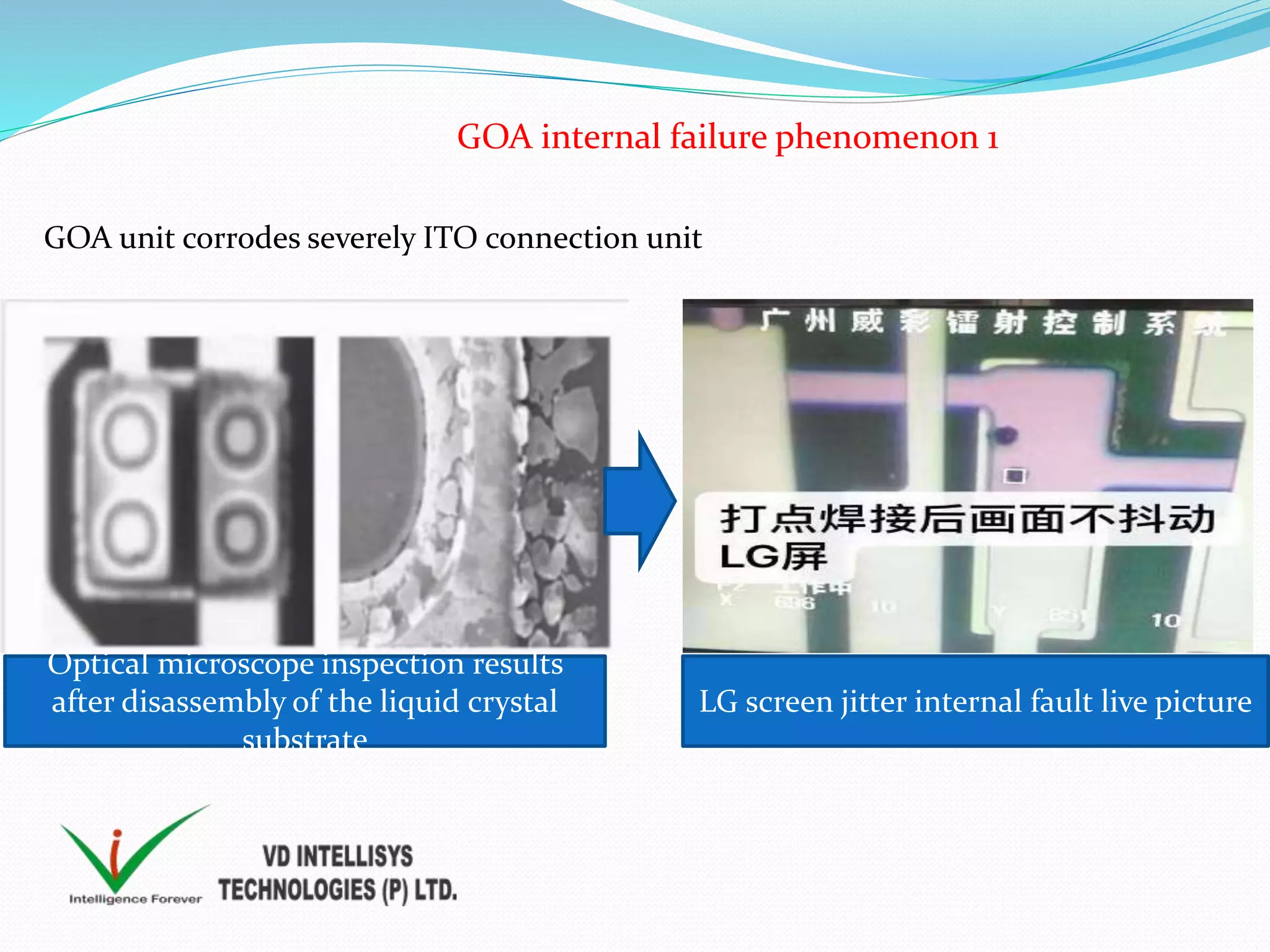
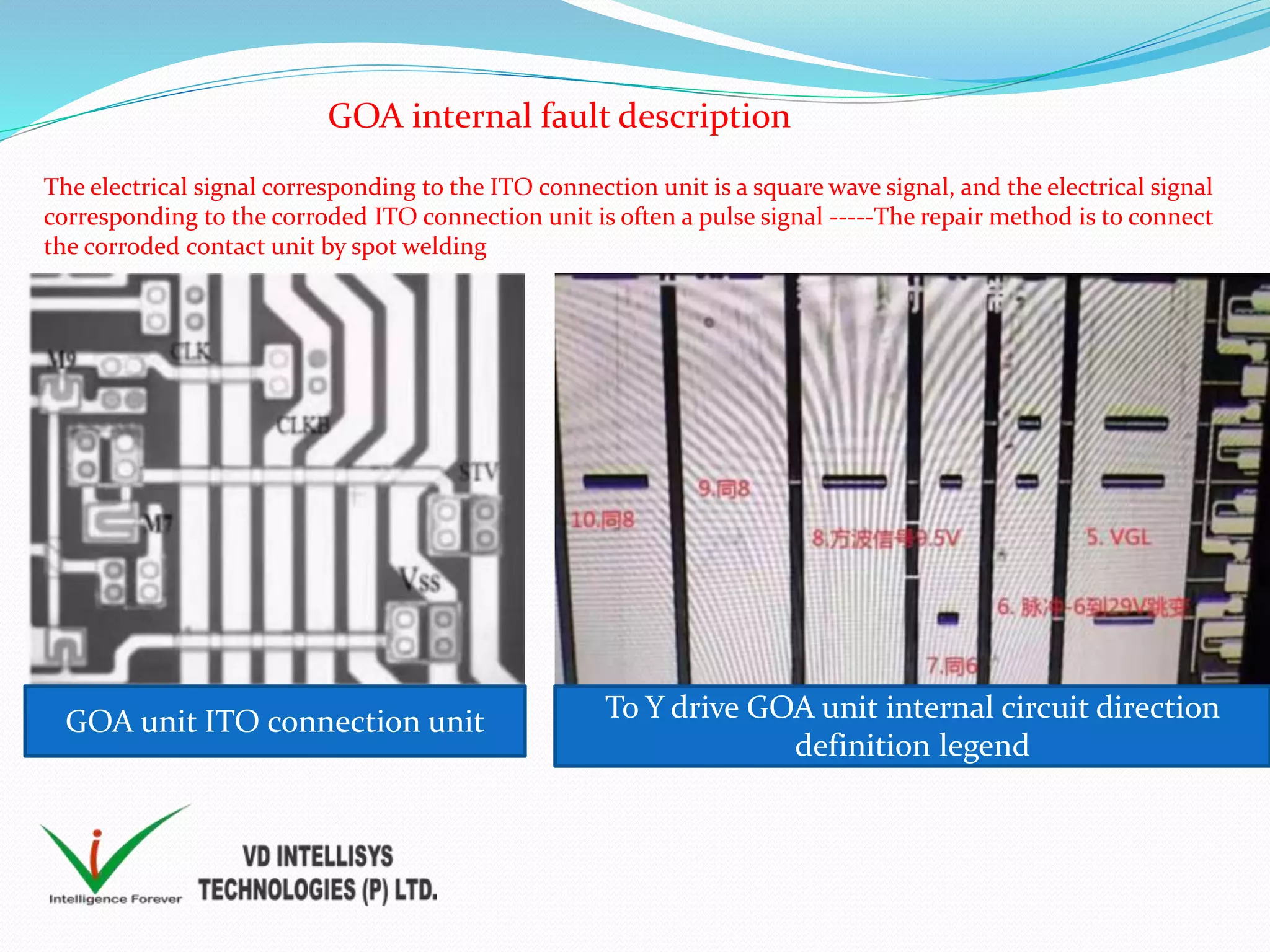
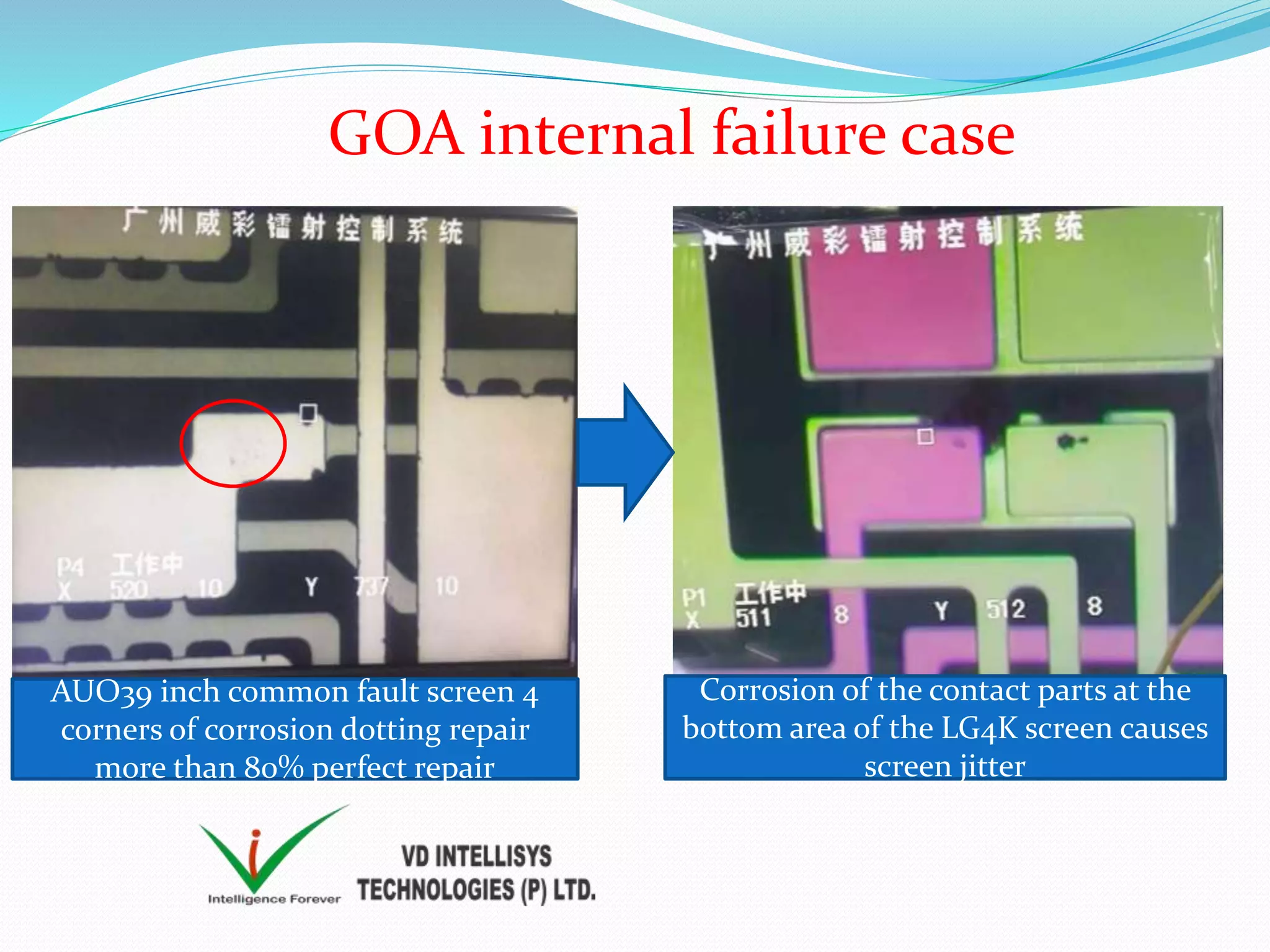
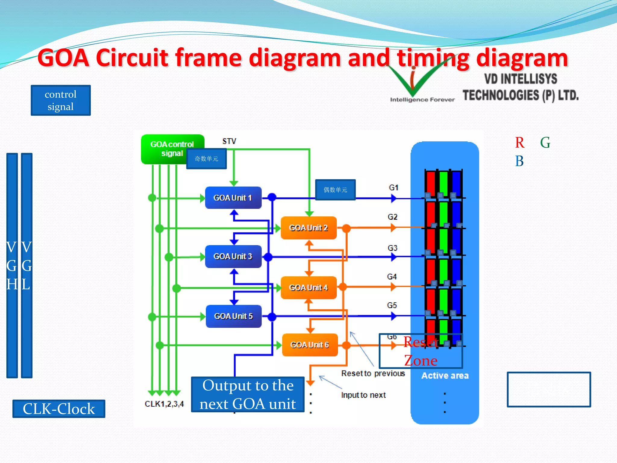
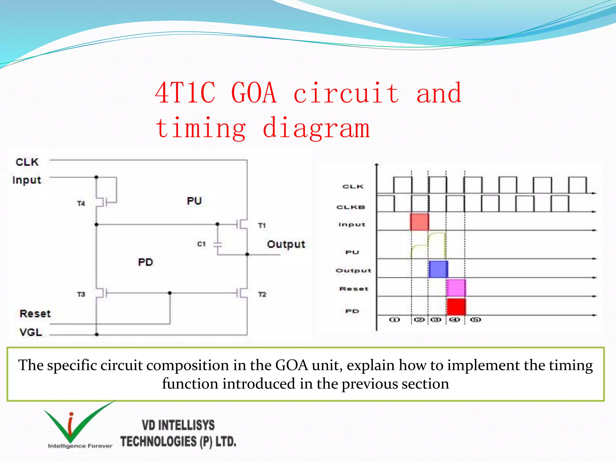
VD Intellisys technologies P LTD.
Laser LCD repair training
2020 Latest Edition
CHIPTRONIKS (Technical Wing)
Prepared by : CHIPTRONIKS LCD TEAM
介绍
LCD screen laser repair machine (referred to as laser machine)
occupies high-end repair technology in the LCD screen repair
industry, and is the highest-end equipment for LCD screen repair.
In the LCD screen repair industry, in addition to TAB loose
soldering, burnt, etc. (this fault can be repaired with a binding
machine) other such as ITO broken wire, ITO scratched, cross line,
bright line, half line, dot line, net Rough parts can be repaired with
a laser machine. The laser machine has the advantages of high
efficiency, high repair rate and low cost in the LCD screen repair
process (the laser machine does not need to replace parts in the
same failure, and the cost is saved and the repair rate is not affected
by the lack of parts). It is widely used As the main screen repair
equipment in large-scale production plants, brand after-sales and
maintenance companies.
Training program
 1. Introduction to the main components of the equipment
and machine operation
 2. Familiar with the internal structure of LCD screen
 3.LCD screen fault classification, common fault analysis
 4.various troubleshooting methods
 5. Special laser repair plan, short-circuit point finding plan
 6. Introduction to GOA circuit structure screen
 7.maintenance case sharing
 8. Equipment debugging method
 9. Routine maintenance of equipment
Laser machine parts introduction
 1. The platform part moves the laser head position in 6 directions into front, back, left,
right, up, down, (focus), and a limit device at the limit position. The moving speed can be
changed by switching between different gears and different gears. Numerical
adjustments are combined and applied.
 2. Water cooler: The function of the water cooler is to cool down the heat generated by
the laser generator flash lamp after laser exposure. The main engine must be powered on
and turned on at the same time to ensure that the water flow of the water cooler
circulates normally. The water in the water tank needs to be replaced with foreign matter
Water and filter cartridge. The water needs to be replaced with pure water.
 3. The laser part is composed of laser power supply + laser generator optical path
components. (Requires familiarity with laser disassembly, optical path lens position
adjustment)
 4. Red light source (marked) and white light source (the brightness of up and down
perspective can be adjusted through the knob)
 5. Light barrier components: control the size and scope of the window by adjusting the X-
axis and Y-axis gate shrinking actions to pass the laser beam.
 6. Eyepiece electric switcher, electric rotating switch of different magnification mirrors
(2X, 5X, 10X mirror observation, 20X laser operation)
Understand some components of laser
machine
 1. Mirror observation: Due to the precise internal circuit structure of the LCD
panel, the internal circuit status needs to be analyzed and observed with high-
resolution mirror images, and the faulty part can be determined and repaired.
Laser machine operation function
description
Adjacent line is ignited, electrical short
circuit
Pixel control circuit sparks to cause bright
lines, internal analysis
 .镜像观察
GOA internal circuit structure
Helps analyze internal circuits and facilitates maintenance
 Mainly used for cutting and trimming micron-sized
components of silicon-based semiconductor circuits,
especially passivation layers (silicon oxide/nitride) and
metal interconnect welding (ITO indium tin oxide).
 The fault is found in the maintenance process because
the circuit is open and requires welding or technical
modification and the cutting function is required to
isolate the faulty circuit.
 Short-circuit caused by bad foreign matter in the
channel requires laser smashing and cleaning.
Function two cutting, welding
Function two :Introduction to cutting
and welding
1. Technical transformation of circuit-
point double-layer welding
2. Technical improvement of the line-
vertical single-layer cutting
3. The contact part of the double-layer
circuit is loose-fixed by welding
Function --- Channel cleaning,
cutting channel
ITO scratches cause electrical
shorts between phases
Circuit re-engineering to
isolate short-circuit area
Poor laser smash
channel
Understanding LCD panel
 1. LCD panel classification:
 1. Constantly bright screen: the pixels are turned on when
there is no electric field, and the LCD screen is white when
illuminated by the backlight. With the power off and no
signal connected, the RGB three primary colors can be clearly
observed using the CCD camera on the laser. The always-on
LCD screen is powered by 3.3V or 5V.
 2. Normally dark screen: the pixels are turned off when there
is no electric field. The LCD screen is black when illuminated
through the backlight. In the state of shutdown and no signal
connection, the CCD camera using laser cannot observe the
three primary colors of RGB. The normally dark LCD screen is
powered by 12V.
Distinguish between always black screen
and always bright screen
R, G, B colors can be seen on the screen
when not working
R, G, B colors cannot be seen on the
screen when not working
Introductio of internal circuit
1
5
4
32
6
7
Introduction of Internal Circuit
ITO
IN
TO
PANEL
Spare
maintenan
ce line 2
Spare
Maintenan
ce LINE 1
线号
Y
Contro
l line
VCOM
Line
X
control
line
Primary Color
pixel unit
Familiar with the direction of PANEL internal circuit, control mode, X/Y/VCOM line,
spare line distinction
Internal pixel unit control type
Samsung horizontal
ladder control
Chimei Innolux vertical
ladder control
LGD longitudinal
step double Y
diagonal control
BOE's vertical first-line
control is one color
1 2 3 4
2. Common faults of LCD panel
 Generally, abnormal display vertical lines appear on the screen, which are
mainly divided into three types: drive signal open circuit and short circuit, or
short circuit of pixels inside the liquid crystal substrate.
 How to judge whether the abnormal line is caused by an external signal or the
inside of the glass?
 1. Normally black screen: The abnormal line displayed on the screen after
lighting is a regular black line from beginning to end is caused by an external
signal.
 2. Constantly bright screen: After lighting, the abnormal line displayed on the
screen is a regular bright line from the beginning to the end, which is caused by
an external signal. .
 3. The abnormal line displayed on the screen of the binding area or COF
package IC area by hand pressing (referred to as hand pressing line) is caused
by external signals. .
 4. Use a microscope to observe the location of the abnormal line area. If two or
more adjacent lines appear abnormally at the same time, it is caused by
external signals. .
 5. Dark lines (weak input signals) are caused by external signals.
 6. Often black screen: the abnormal line displayed on the
screen after lighting is irregular black line from beginning
to end is caused by the inside of the glass.
 7. Constant bright screen: After lighting, the abnormal line
displayed on the screen is caused by the inside of the glass
if the irregular bright line is displayed from the beginning
to the end.
 8. Irregular lines are small and large lines, half lines, and
cross lines are all caused by PANEL internal pixel unit
problems. Commonly caused by control circuit capacitance,
MOS tube leakage, short circuit breakdown, and poor
performance of the insulation layer between control lines.
 Horizontal lines ---- Reasons for abnormal horizontal lines on
the screen:
 1. Poor contact between COF COG and glass due to poor contact
and lack of drive signal.
 2. COF IC/line, COG itself is defective, damaged, etc. which
cause loss of drive signal.
 3. The ITO electrode is corroded, and the open circuit of the
broken wire causes the lack of driving signal.
 Foreign matter and dirty spots in the terminal binding area cause
a short circuit of the drive signal.
 4. Short-circuit, capacitance, and leakage of pixel points in the
substrate.
 5. The GOA circuit fault is caused by a short circuit associated
with the signal.
 Cross line---This fault is caused by the short circuit of the internal
circuit of the LCD substrate. The X control line and the Y control line
are short-circuited at a certain intersection to form two lines, one
vertical and one horizontal. A bright spot can be seen at the
intersection (the bright spot is actually a faulty part). The repair
method after finding the faulty pixel Find the bright spots of abnormal
pixels under the 20X microscope of the laser machine. Use the laser to
cut the faulty pixels from the main line control line before the signal
input end of the abnormal pixel unit. This will no longer affect the
normal operation of the main line. The faulty pixels will change after
isolation. The repair method to repair the bright spots to black spots is
(see the solution below). If the faulty pixel input terminal failure still
exists after partial cutting, the faulty pixel unit of the main line control
line must be separated by laser cutting before and after it. After that, it
will become a semi-abnormal line display. Refer to the above for the
half-line maintenance method.
 The size of the head line---the reason is that the X control line or the Y control line is
short-circuited between the pixel unit and the substrate backplane (VCOM). The
position of the visual short circuit is relatively unobvious near the COF drive. The
abnormal line is weaker, and the closer the short circuit point The more obvious the
abnormal line is.
 Half line---This fault is generally caused by an open circuit in the internal control circuit
of the substrate. The X-axis control line or the Y-axis control line is open somewhere, and
the drive signal is not available in the second half after the open circuit, so the second
half does not work. , Forming a half of the abnormal half line fault appears at the
junction of the abnormal line and the normal display line.
 Bright spots---There are bright spots on the screen when using a dark picture, and the
dots RGB color and orientation are different. This fault is generally caused by poor TFT
on the pixel (PANEL drive MOS tube open circuit) or foreign matter in the pixel. The
repair method is to find the abnormal pixel bright spot under the 20X microscope of the
laser machine and use the laser to weld the internal ground of the pixel. The pixel will
turn off and become a black spot under the influence of the signal, and the black spot is
often more acceptable to customers.
Operation and maintenance methods: (operating equipment)
 Often dark screen
 Broken lines (vertical and horizontal lines):
 1. Complete black line (fault line caused by external signal)
 Find broken wires and repair methods:
 A. Connect the LCD panel to be repaired and connect to the VGA signal, use the NOKIA
screen measurement software to open the RGB conversion option and turn to the white
interface.
 B. When the black abnormal line is observed, the laser head position movement action of
the laser machine will switch the 20 times objective lens of the laser machine, adjust the
brightness of the white light source to the maximum, and aim the white light spot at the
top of the broken line (COF end)
 C. Change the objective lens of the laser machine to 5 times to observe more internal
circuits of the panel. Under the normal power-on state, all the three primary colors of
RGB will be displayed normally. Quickly find the display area that does not have any RGB
three primary colors and is black is the location of the abnormal line.
Connect
 D. After determining the abnormal line area, observe the line structure to
quickly find the control x-direction line corresponding to the abnormal
line, and follow the control line to the spare line area of the panel.
 Repair method: The connection method of the vertical line is to use laser
spot welding to connect the two layers of the spare line in the area where
the abnormal line corresponds to the spare line, and then follow the RGB
three-base arrangement order, up or down from the second line. After
reaching the sixth spare wire area of the same color (some 4K screens are
calculated to reach the eighth with 4 primary colors), then do spot welding.
After the welding is completed, the both ends of the spare wire must be cut
off at the abnormal wire and wiring position. If it is found that there is no
spare repair line type screen or the spare repair line is not enough, the Y
horizontal signal line can generally be borrowed. The welding method is
the same. After welding, the two ends of the borrowed area must be
undercut and cut off.
接上
 The horizontal line is connected according to the RGB
arrangement sequence, starting from the second line up or
down, reaching the second spare line area of the same color
and then performing dot welding. If there is no spare repair
line type screen or If the spare maintenance line is not
enough, the X vertical signal line can generally be
borrowed. The welding method is the same. After welding,
the two ends of the borrowed area must be undercut and
cut off. Part of the GOA circuit type screen (the Y-side
control circuit is designed in the glass inner layer) has a
horizontal line. It is necessary to find one of the faulty
sides. Use a laser to cut the fault signal to isolate the fault
location.
接上
半线(黑色)
 2. Half line (black)
 A. Connect the LCD panel to be repaired and connect to the VGA signal, use the NOKIA screen
measurement software to open the RGB conversion option and turn to the white interface.
 B. After observing the half-line area and using the 20x objective lens of the laser machine,
adjust the brightness of the white light source to the maximum, and aim the white light spot at
the broken line (damage one end)
 C. Change the objective lens of the laser machine to 5 times to observe more internal circuits of
the panel. Under the normal power-on state, all the three primary colors of RGB will be
displayed normally. Quickly find the display area that does not have any RGB primary colors
and is black is the location of the bad line.
 D. After determining the bad line area, observe the line structure to quickly find the
corresponding control line, and follow the control line to the spare line area of the panel
 Repair method: The half line connection method is to repair the damaged end of the broken
line. Use laser dot welding to connect the two layers of the spare line in the area corresponding
to the spare line, and then follow the RGB arrangement order, starting from the second line up
or down, and reach the sixth spare line area of the same color. Do spot welding. After the
welding is completed, cut off the area of the abnormal line, and the connected line must be cut
off at the position of the upper six lines.
 X or Y is short-circuited with the backplane (VCOM) somewhere. Depending on the short-
circuit position, the line near the COF drive is relatively inconspicuous, and the line closer to
the short-circuit point is more obvious. In the case where the short-circuit point cannot be
visually inspected or cannot be found, carefully observe the position of the line thickness and
the thin line and the color depth of the upper and lower parts of the bright line. The area with
the general line thickness and dark color is the approximate short-circuit point area.
 Maintenance plan: According to the area where the short circuit is judged, drag the short
circuit point in the direction of the bottom of the panel or the COF end by dragging the short
circuit point and let it appear.
 Operation 1: Follow the half-line repair method to repair the area where the line is obviously
bad. After the connection and partition are completed, two bright spots will appear near the
broken line in the entire screen display area.
 Operation 2: Use the laser microscope to quickly find the location of the bright spot and align
it, and walk along the location of the bright spot to the direction of the broken line to find the
short-circuit point
 Operation 3. After finding the short-circuit point, use the laser to cut the short-circuit position
up and down. After the processing is completed, the image will appear half-line, and then
follow the half-line repair method.
 Remarks: Some panels still have residual dark lines after the repair is completed. You can turn
off the power for a period of time and then reconnect the power to observe, the dark lines will
basically disappear. This is a process that needs to be discharged after the repair.
Find the short-circuit pixel method
 1. Visual observation method: carefully observe the
abnormal line from top to bottom and scan the state of a
pixel point differently than other abnormal lines (obviously
black spots, obvious bright spots, obvious flashing points,
obvious weaknesses), and it can be judged as Abnormal
failure point.
 2. Power-off method: stare at the abnormal line area by
disconnecting the power supply of the drive motherboard
screen and then see if there is a residual bright spot on one
of the pixels (some abnormal bright spots will show slower
response during charging and discharging. Situation) can
be determined as an abnormal fault point.
 3. A cross line or a dark horizontal line is the abnormal
fault point at the cross section.
Connect
 4. Percussion method: The panel can be slightly lifted to tap or tap the
abnormal line part slightly. During the tapping process, carefully observe
whether there are abnormally obvious black spots, obvious bright spots,
obvious flashing points, obvious weak points or very The dark cross-hairs exist
because some control circuits have slight leakage and breakdown on the glass
substrate. External distortion and external forces can make the fault point
more obvious and determine the fault location.
 5. Bridging method: In the case that no abnormal fault point is found after
trying the above methods, we can bridge the internal signal of the glass. The
method to find is to find the abnormal fault line at the end (the other end in
the COF direction) Do spot welding across the spare repair line on the
abnormal line, then (RGB) to the sixth line for welding, and then to the twelfth
and 18th lines for welding. After welding, go and observe. At this time, the
screen will show several abnormal lines Observe carefully whether there are
obvious black spots, obvious bright spots, obvious flashing points, obvious
weaknesses and other bad fault points on the original abnormal fault line.
Connect
 6. The electric shock method uses a high-voltage electric
rod to scan the abnormal line area. Through external high-
voltage interference, the internal circuit pixels will show
different states, which helps to accurately find the
abnormal pixels. Some of the slight dark lines are due to
slight internal leakage. It is possible to return to normal
after high-voltage interference. When using high-voltage
electric rods, please be careful to stay away from the COF
end as far as possible. Some COF performance is poor and
there is a risk of IC burnout.
 7. Distinguish regional mirroring and regional scanning,
observe and find out the fault point.
Precautions for using laser repair process:
 Precautions for using laser repair process:
 1. Pay attention to check whether the cooling water can circulate normally after starting the machine
every day. In cold areas, it must be ensured that the cooling water does not freeze. If it is accidentally
frozen, the cooling water can be used after normal circulation after thawing.
 2. Power value adjustment: Generally, the power value can be adjusted so that green light can be
normally generated when the laser is excited, and it can be adjusted to a higher value of 1-2 when the
laser is generated.
 3. When cutting and welding inside the glass pixel, pay attention to adjusting the smallest laser spot
as much as possible. The cutting and welding position must be moved accurately. The position after
the laser must be pre-judged, and the laser welding or cutting operation must not cause other phase
The adjacent circuit is damaged.
 4. It is predicted that the external signal is abnormal and the bridging method is welded. When the
fault shows two lines, it is necessary to distinguish whether the 2 heads of the spare repair line are not
cut clean or the input abnormal signal is not cut clean or the fault line is caused by the inside of the
glass. The other is the borrowed spare The line cannot be used.
Connect
 5. Spot welding The general welding position is to do spot welding at the diagonal
position of the overlap area. Adjust the appropriate laser spot size according to the panel
circuit material and the size of the welding line to perform welding operations, and try to
preserve the integrity of the transmission line after the welding is completed.
 6. The method of repairing the bright spot into a black spot is to find the bottom line at
the corresponding position of the fault bright spot and then weld it to the ground wire to
discharge the fault bright spot.
 7. Welding and cutting must be clearly confirmed before the operation, especially the
cutting operation. If the signal line after cutting is judged incorrectly, it cannot be
restored to the previous one before cutting.
 8. The general processing method of the GOA screen is to determine whether the fault is
caused by the left circuit or the right circuit, and input the fault side circuit into each
power supply and signal line for cutting and isolation. After isolation, the abnormal
horizontal line should be input to the fault end. The front end of the capacitor is cut and
isolated, and part of the horizontal line of the GOA screen can be repaired by bridging
the third signal line.
Connect
 9. The COF and COG schemes produce abnormal horizontal line
external signals to cause the general bridging method to be welded to
the second one at the other.
 10. The vertical lines caused by external signals are processed by
bridging the three primary colors. Connect the 6th 120HZ screen.
Partially connect to the 12th. If there is a dark line after the 6th is
connected, the 6th and 12th can be connected at the same time. If the
screen with 4 primary colors is connected to the 8th or 16th, the 8th
and 16th lines can be connected at the same time.
 11. To analyze the circuit, it is necessary to clearly distinguish whether
the faulty abnormal line is caused by external signals or caused by the
inside of the glass. The processing methods are different.
 12. After repairing, some dark lines must be clarified whether it is
caused by unclean cutting abnormal signal connection or weak bridge
drive signal or some screens need to be placed for a period of time
before the dark lines disappear by themselves.
Pixel abnormal bright line connection A method (Panda, Sharp
structure)
An irregular bright line is always on
when the screen is gray
The insulation layer of X and Y control lines breaks and sparks. Cut
the input and output ends of the X control line to isolate the fault
point, and the front end returns to normal and the back half line
Go to the bottom of the screen to find the
outermost part of the spare line for welding
Follow the spare line to the left or right to
find the winding contact point for welding
To the COF end corresponding to the wire
number and spare wire to do spot welding
until the signal is turned on
Schematic diagram of the direction of the short-circuit line connected to the A line caused by the
faulty pixel
Note: The faulty pixel must be judged accurately, analyze the circuit to find the best cutting point, and cut clean without hurting other
pixels. It depends on whether the circuit structure is repaired by internal winding or external winding or grayscale connection.
Outlier
Schematic diagram of open vertical wire connection
method
Not
worki
ng
R G B R (malfunction) G B R G B
R
备用线
Schematic diagram of open
horizontal line wiring method备用线
不工作(异常线)
12
Remarks: There is an external Y horizontal line that is basically welded at intervals.
Many outside Y have no spare repair lines, and only the outermost X control line
can be used for repair.
GOA learning
 1. Introduction to GOA driving principle
 (1). GOA (gate on array) technology: a technology that uses thin film
transistor technology to integrate gate drive circuits on Array glass.
 (2). Advantages of GOA:
 a) Cost reduction: It saves Gate IC and is mainly suitable for large size;
 b) Module process yield & yield improvement: no Gate IC bonding;
 c) Realization of narrow border: Suitable for Mobile high-resolution
products.
 (3). Key technology: shift register (shift register)
 2. Detailed explanation of GOA frame structure and drive timing:
 The function of the GOA circuit is to sequentially output a high-level
square wave to the gate lines of each row within a frame time, and turn
on the pixel TFTs corresponding to these gate lines row by row, so that
the data line can complete a charge and refresh for all sub-pixels in the
pixel area.
GOA Circuit frame diagram and timing diagram
CLK-Clock
control
signal
奇数单元
偶数单元
活动区
Reset
Zone
Output to the
next GOA unit
V
G
H
V
G
L
R
Connect
 In general GOA design, GOA circuits are arranged at both ends of the gate line, so
that the Panel can have a symmetrical width, which is convenient for design and
process flow, and also meets the requirements of the end product for FPD (flat
panel display) products.
 For small-size FPD products, due to the relatively small load of the gate lines, GOA
cross-drive can generally be used, that is, GOA drives the odd-numbered gate lines
on one side and the even-numbered gate lines on the other side. The left and right
sides do not interfere with each other. Staggered to achieve the effect of sequentially
turning on the gate lines, which is called unilateral driving, which can save frame
width and power consumption.
 For medium and large size FPD products, due to the large load of the gate line, in
order to normally turn on the gate line, GOA usually adopts bilateral driving, that is,
for a row of gate lines, there will be a GOA unit on the left and right sides to charge
it. In this case, the left and right GOA circuit design is completely symmetrical,
which is called bilateral drive.
 Figure 1-1 is a GOA frame diagram and timing diagram (only the left half is drawn,
assuming this example is a bilateral drive), the following uses the GOA circuit as an
example to illustrate the working timing principle of GOA
(1)GOA电路的输入信号
 (1) The input signal of GOA circuit:
 a) Clock signal: one or more groups, each group contains complementary CLK
and CLKB (clock pulse) signals, each group of clock signals corresponds to a
group of GOA units, in this example there are 2 groups of GOA signals,
CLK1&CLK3 are complementary, corresponding to odd groups GOA unit,
CLK2&CLK4 are complementary, corresponding to even group GOA unit, as
shown in the timing diagram on the right.
 b) Constant voltage signal: high-level VGH, low-level VGL, generally one VGH
and one VGL are required. Depending on the circuit structure in the GOA unit,
multiple VGH or VGL signals may not be needed or required (because each
GOA The constant voltage signal type and connection mode required by the
unit are the same, so it is not shown in the figure).
 Turn-on signal: the input signal STV required by the first GOA unit of each
group of GOA units. Depending on the GOA circuit structure, one or more STV
signals are required. In this example, 2 groups of GOA units only need one set
of STV signals
(2)GOA The output signal of the circuit :
 (2) The output signal of GOA circuit:
 Sequentially output square wave pulses to each gate line (shift register
function), such as G1~G6 in Figure 1-x (to the control pixel Y line).
 (3) Introduction of GOA unit (GOA unit 1~6 etc.):
 a) The opening conditions of GOA unit:
 The CLK signal connected to a GOA unit will periodically appear a high-
level square wave. When the CLK appears a high-level square wave, the
GOA unit will output a high-level square wave and turn on the gate line
when the following two conditions are met. Connected pixel TFT:
 Before the high-level square wave, the row of GOA receives the ON signal
input by the INPUT signal. For the first GOA unit of each group of GOA
(GOA unit 1 & 2 in this example), the INPUT signal is the STV provided by
the control unit Signal. For the remaining GOA units, the INPUT signal is
provided by the output of the previous GOA unit in this group of GOA, as
shown in the figure "Input to next".
Connect
 ii. Before the high-level square wave, the row of GOA did not receive the close
signal input by the RESET signal. For the last GOA unit of each group of GOA
(not shown in this example), the RESET signal is determined by the next GOA
in the group The output of the GOA unit is provided, as shown in the figure
"Reset to previous". In particular, for the last GOA unit of each group of GOA,
since it is already the last GOA unit, additional circuit design is needed for it
Provide RESET signal.
 b) The output of each GOA unit:
 i. If the above two conditions are met, the GOA outputs a high-level square
wave and turns on the pixel TFT above the gate line.
 ii. Its output will also be connected to the previous GOA unit in this group of
GOA as a RESET signal, which is used to turn off the output of the previous
GOA unit (the first GOA unit does not need to output a RESET signal).
 iii. Its output will also be connected as INPUT signal to the next GOA unit in
this group of GOA, which is used to turn on the next GOA unit after the
corresponding opening time of GOA in this row ends (the last GOA unit does
not need to output INPUT signal).
(4) Timing description:
 a) Combining the above explanation of each unit and signal, explain the overall working
sequence of GOA:
 After a frame starts, the control unit inputs the required STV signal and CLK signal to the GOA
circuit. The first GOA unit of each group of GOA receives the STV signal, and when the
corresponding CLK is high, it outputs a high-level square wave, such as timing In G1&G2 of the
figure, the output is not only used to turn on its corresponding gate line, but also acts as an
INPUT signal on the next GOA unit.
 Starting from the second GOA unit of each group of GOA, the subsequent GOA unit receives
the INPUT signal provided by the previous GOA unit, and when the corresponding CLK is high,
it outputs a high-level square wave. This output is not only used for its corresponding gate The
opening of the polar line also acts as an INPUT signal on the next GOA unit, and also acts as a
RESET signal on the previous GOA unit. This continues until the end of the last GOA output
(as mentioned above, the last GOA does not need to output INPUT).
 Each GOA unit will turn off the GOA output of the previous line in the same group when the
output of this line starts, and the next line of GOA will also start output and close the output of
this line after the output of this line is finished. In this way, each group of GOA is OK Realize
sequential output and realize the function of shift register. For example, in the timing diagram,
the G1-G3-G5 sequence has no overlapping output, and the G2-G4-G6 sequence has no
overlapping output.
Method of using multiple sets of GOA units
 b) Method of using multiple sets of GOA units:
 It can be seen from the timing diagram that the second group of CLK (CLK2 &
CLK4) is delayed by half the square wave width relative to the first group of
CLK (CLK1 & CLK3), which causes its output to be relatively delayed by half the
width. The overlap between group outputs, in order to ensure normal pixel
charging, the specific method is:
 i. Set the STV time and CLK square wave width to be twice the actual turn-on
time of each row of gate lines (H in the figure represents the actual turn-on
time allocated for each row of gate lines).
 ii. Each time the pixel is charged only in the second half of the time when the
gate line is turned on, as shown in the area occupied by the gray boxes on each
output waveform.
 c) Reasons for using multiple GOA units:
 i. Reduce power consumption
 ii. Improve driving ability
 The disadvantage is that it will increase the width of the frame and the number
of incoming signal lines, which needs to be weighed in the design.
(5) GOA circuit frame diagram and timing diagram
of unilateral drive
The framework diagram and timing diagram of 4CLK unilateral drive GOA are
similar to the principle of bilateral drive 4CLK described above
Left Right
2 2.5 3 3.5
4T1C GOA circuit and
timing diagram
The specific circuit composition in the GOA unit, explain how to implement the timing
function introduced in the previous section
 The working principle of 4T1C GOA unit circuit.
 Step ①: No Input signal is input to the GOA unit, although the CLK voltage will appear
high, but because the PU point maintains a low voltage, TFT T1 is off, and GOA has no
output.
 Step ②: Input signal (Generally, the Input of the GOA unit is Output[N-1], and the Input
of the GOA unit in the first row is STV) input through T4, make the PU point change to
high level, M3 is turned on, but at this time CLK is in Low level, so GOA still has no
output.
 Step ③: CLK changes to high level. Since the PU point is already high, T1 is turned on
and Output will output high level. Due to the existence of capacitor C1 and the parasitic
capacitance of T1 itself, as the output potential rises High, the potential of the PU point
will be further raised, so that T1 will be turned on more, further improving the charging
capacity of T1 and ensuring pixel charging.
 Step ④: CLK becomes low level, RESET becomes high level, PD point is raised, and T2
and T3 are turned on, PU point and Output are pulled low by VGL, and the output is
turned off.
 Step ⑤: Return to the state of step ① and keep no output until the next frame is scanned.
GOA circuit failure causes abnormal picture
phenomenon
The malfunction of the GOA working
circuit will cause the screen to be
abnormal, such as gray screen, flashing,
horizontal rough lines, horizontal screen
jumping up and down (shaking screen),
single horizontal line, multiple
horizontal lines, slow screen response,
and normal display of the remaining area
in the horizontal area. Cannot display
normally, etc.
Common situations of GOA circuit problems
 1. The edges of the ITO connection unit have different
degrees of corrosion. These units include gate start
signal (STV) output holes, turn-off voltage (VSS)
signal output holes, input signal (Input) signal
connection holes, and reset (RESET) signal
connections Holes and output signal connection holes,
these severely corroded ITO units, with a microscope,
it can be found that the edges of the connection parts
are severely corroded, which often leads to the direct
reason that the GOA signal cannot be conducted
normally.
GOA internal failure phenomenon 1
Optical microscope inspection results
after disassembly of the liquid crystal
substrate
LG screen jitter internal fault live picture
GOA unit corrodes severely ITO connection unit
GOA internal fault description
The electrical signal corresponding to the ITO connection unit is a square wave signal, and the electrical signal
corresponding to the corroded ITO connection unit is often a pulse signal -----The repair method is to connect
the corroded contact unit by spot welding
GOA unit ITO connection unit To Y drive GOA unit internal circuit direction
definition legend
GOA internal failure case
AUO39 inch common fault screen 4
corners of corrosion dotting repair
more than 80% perfect repair
Corrosion of the contact parts at the
bottom area of the LG4K screen causes
screen jitter
 1. Carefully observe the internal mirror image of the screen
to avoid some small flaws.
 2. The four corner circuits of the screen are the key points
to check for abnormalities in the entire screen in the high-
prone area of failure.
 3. Look for high temperature parts, there are bubbles,
corrosion, burning spots inside the mirror.
 4. GOA circuit corresponding to normal and abnormal
areas of the screen
 5. Find out the problem of the same type of failure and the
same part of the same model regularly, and observe the
improvement of the picture during the repair process.
Maintenance experience
GOA internal failure phenomenon two
CLK input line is easy to cause ignition and short circuit due to the
design line distance is too small
Use laser to transform lines and increase line safety distance
上Layer circuit and lower layer circuit breakdown and short
circuit need to be cut or technically modified.
Multiple groups of pulse signals are short-circuited, and the thick
connection is repaired after cutting
Maintenance case sharing one
接上
接上
维修案例分享二
接上
接上

Laser machine vd512 e training

  • 1.
    VD Intellisys technologiesP LTD. Laser LCD repair training 2020 Latest Edition CHIPTRONIKS (Technical Wing) Prepared by : CHIPTRONIKS LCD TEAM
  • 2.
    介绍 LCD screen laserrepair machine (referred to as laser machine) occupies high-end repair technology in the LCD screen repair industry, and is the highest-end equipment for LCD screen repair. In the LCD screen repair industry, in addition to TAB loose soldering, burnt, etc. (this fault can be repaired with a binding machine) other such as ITO broken wire, ITO scratched, cross line, bright line, half line, dot line, net Rough parts can be repaired with a laser machine. The laser machine has the advantages of high efficiency, high repair rate and low cost in the LCD screen repair process (the laser machine does not need to replace parts in the same failure, and the cost is saved and the repair rate is not affected by the lack of parts). It is widely used As the main screen repair equipment in large-scale production plants, brand after-sales and maintenance companies.
  • 3.
    Training program  1.Introduction to the main components of the equipment and machine operation  2. Familiar with the internal structure of LCD screen  3.LCD screen fault classification, common fault analysis  4.various troubleshooting methods  5. Special laser repair plan, short-circuit point finding plan  6. Introduction to GOA circuit structure screen  7.maintenance case sharing  8. Equipment debugging method  9. Routine maintenance of equipment
  • 4.
    Laser machine partsintroduction
  • 5.
     1. Theplatform part moves the laser head position in 6 directions into front, back, left, right, up, down, (focus), and a limit device at the limit position. The moving speed can be changed by switching between different gears and different gears. Numerical adjustments are combined and applied.  2. Water cooler: The function of the water cooler is to cool down the heat generated by the laser generator flash lamp after laser exposure. The main engine must be powered on and turned on at the same time to ensure that the water flow of the water cooler circulates normally. The water in the water tank needs to be replaced with foreign matter Water and filter cartridge. The water needs to be replaced with pure water.  3. The laser part is composed of laser power supply + laser generator optical path components. (Requires familiarity with laser disassembly, optical path lens position adjustment)  4. Red light source (marked) and white light source (the brightness of up and down perspective can be adjusted through the knob)  5. Light barrier components: control the size and scope of the window by adjusting the X- axis and Y-axis gate shrinking actions to pass the laser beam.  6. Eyepiece electric switcher, electric rotating switch of different magnification mirrors (2X, 5X, 10X mirror observation, 20X laser operation) Understand some components of laser machine
  • 6.
     1. Mirrorobservation: Due to the precise internal circuit structure of the LCD panel, the internal circuit status needs to be analyzed and observed with high- resolution mirror images, and the faulty part can be determined and repaired. Laser machine operation function description Adjacent line is ignited, electrical short circuit Pixel control circuit sparks to cause bright lines, internal analysis
  • 7.
     .镜像观察 GOA internalcircuit structure Helps analyze internal circuits and facilitates maintenance
  • 8.
     Mainly usedfor cutting and trimming micron-sized components of silicon-based semiconductor circuits, especially passivation layers (silicon oxide/nitride) and metal interconnect welding (ITO indium tin oxide).  The fault is found in the maintenance process because the circuit is open and requires welding or technical modification and the cutting function is required to isolate the faulty circuit.  Short-circuit caused by bad foreign matter in the channel requires laser smashing and cleaning. Function two cutting, welding
  • 9.
    Function two :Introductionto cutting and welding 1. Technical transformation of circuit- point double-layer welding 2. Technical improvement of the line- vertical single-layer cutting 3. The contact part of the double-layer circuit is loose-fixed by welding
  • 10.
    Function --- Channelcleaning, cutting channel ITO scratches cause electrical shorts between phases Circuit re-engineering to isolate short-circuit area Poor laser smash channel
  • 11.
    Understanding LCD panel 1. LCD panel classification:  1. Constantly bright screen: the pixels are turned on when there is no electric field, and the LCD screen is white when illuminated by the backlight. With the power off and no signal connected, the RGB three primary colors can be clearly observed using the CCD camera on the laser. The always-on LCD screen is powered by 3.3V or 5V.  2. Normally dark screen: the pixels are turned off when there is no electric field. The LCD screen is black when illuminated through the backlight. In the state of shutdown and no signal connection, the CCD camera using laser cannot observe the three primary colors of RGB. The normally dark LCD screen is powered by 12V.
  • 12.
    Distinguish between alwaysblack screen and always bright screen R, G, B colors can be seen on the screen when not working R, G, B colors cannot be seen on the screen when not working
  • 13.
    Introductio of internalcircuit 1 5 4 32 6 7
  • 14.
    Introduction of InternalCircuit ITO IN TO PANEL Spare maintenan ce line 2 Spare Maintenan ce LINE 1 线号 Y Contro l line VCOM Line X control line Primary Color pixel unit Familiar with the direction of PANEL internal circuit, control mode, X/Y/VCOM line, spare line distinction
  • 15.
    Internal pixel unitcontrol type Samsung horizontal ladder control Chimei Innolux vertical ladder control LGD longitudinal step double Y diagonal control BOE's vertical first-line control is one color 1 2 3 4
  • 16.
    2. Common faultsof LCD panel  Generally, abnormal display vertical lines appear on the screen, which are mainly divided into three types: drive signal open circuit and short circuit, or short circuit of pixels inside the liquid crystal substrate.  How to judge whether the abnormal line is caused by an external signal or the inside of the glass?  1. Normally black screen: The abnormal line displayed on the screen after lighting is a regular black line from beginning to end is caused by an external signal.  2. Constantly bright screen: After lighting, the abnormal line displayed on the screen is a regular bright line from the beginning to the end, which is caused by an external signal. .  3. The abnormal line displayed on the screen of the binding area or COF package IC area by hand pressing (referred to as hand pressing line) is caused by external signals. .  4. Use a microscope to observe the location of the abnormal line area. If two or more adjacent lines appear abnormally at the same time, it is caused by external signals. .  5. Dark lines (weak input signals) are caused by external signals.
  • 17.
     6. Oftenblack screen: the abnormal line displayed on the screen after lighting is irregular black line from beginning to end is caused by the inside of the glass.  7. Constant bright screen: After lighting, the abnormal line displayed on the screen is caused by the inside of the glass if the irregular bright line is displayed from the beginning to the end.  8. Irregular lines are small and large lines, half lines, and cross lines are all caused by PANEL internal pixel unit problems. Commonly caused by control circuit capacitance, MOS tube leakage, short circuit breakdown, and poor performance of the insulation layer between control lines.
  • 18.
     Horizontal lines---- Reasons for abnormal horizontal lines on the screen:  1. Poor contact between COF COG and glass due to poor contact and lack of drive signal.  2. COF IC/line, COG itself is defective, damaged, etc. which cause loss of drive signal.  3. The ITO electrode is corroded, and the open circuit of the broken wire causes the lack of driving signal.  Foreign matter and dirty spots in the terminal binding area cause a short circuit of the drive signal.  4. Short-circuit, capacitance, and leakage of pixel points in the substrate.  5. The GOA circuit fault is caused by a short circuit associated with the signal.
  • 19.
     Cross line---Thisfault is caused by the short circuit of the internal circuit of the LCD substrate. The X control line and the Y control line are short-circuited at a certain intersection to form two lines, one vertical and one horizontal. A bright spot can be seen at the intersection (the bright spot is actually a faulty part). The repair method after finding the faulty pixel Find the bright spots of abnormal pixels under the 20X microscope of the laser machine. Use the laser to cut the faulty pixels from the main line control line before the signal input end of the abnormal pixel unit. This will no longer affect the normal operation of the main line. The faulty pixels will change after isolation. The repair method to repair the bright spots to black spots is (see the solution below). If the faulty pixel input terminal failure still exists after partial cutting, the faulty pixel unit of the main line control line must be separated by laser cutting before and after it. After that, it will become a semi-abnormal line display. Refer to the above for the half-line maintenance method.
  • 20.
     The sizeof the head line---the reason is that the X control line or the Y control line is short-circuited between the pixel unit and the substrate backplane (VCOM). The position of the visual short circuit is relatively unobvious near the COF drive. The abnormal line is weaker, and the closer the short circuit point The more obvious the abnormal line is.  Half line---This fault is generally caused by an open circuit in the internal control circuit of the substrate. The X-axis control line or the Y-axis control line is open somewhere, and the drive signal is not available in the second half after the open circuit, so the second half does not work. , Forming a half of the abnormal half line fault appears at the junction of the abnormal line and the normal display line.  Bright spots---There are bright spots on the screen when using a dark picture, and the dots RGB color and orientation are different. This fault is generally caused by poor TFT on the pixel (PANEL drive MOS tube open circuit) or foreign matter in the pixel. The repair method is to find the abnormal pixel bright spot under the 20X microscope of the laser machine and use the laser to weld the internal ground of the pixel. The pixel will turn off and become a black spot under the influence of the signal, and the black spot is often more acceptable to customers.
  • 21.
    Operation and maintenancemethods: (operating equipment)  Often dark screen  Broken lines (vertical and horizontal lines):  1. Complete black line (fault line caused by external signal)  Find broken wires and repair methods:  A. Connect the LCD panel to be repaired and connect to the VGA signal, use the NOKIA screen measurement software to open the RGB conversion option and turn to the white interface.  B. When the black abnormal line is observed, the laser head position movement action of the laser machine will switch the 20 times objective lens of the laser machine, adjust the brightness of the white light source to the maximum, and aim the white light spot at the top of the broken line (COF end)  C. Change the objective lens of the laser machine to 5 times to observe more internal circuits of the panel. Under the normal power-on state, all the three primary colors of RGB will be displayed normally. Quickly find the display area that does not have any RGB three primary colors and is black is the location of the abnormal line.
  • 22.
    Connect  D. Afterdetermining the abnormal line area, observe the line structure to quickly find the control x-direction line corresponding to the abnormal line, and follow the control line to the spare line area of the panel.  Repair method: The connection method of the vertical line is to use laser spot welding to connect the two layers of the spare line in the area where the abnormal line corresponds to the spare line, and then follow the RGB three-base arrangement order, up or down from the second line. After reaching the sixth spare wire area of the same color (some 4K screens are calculated to reach the eighth with 4 primary colors), then do spot welding. After the welding is completed, the both ends of the spare wire must be cut off at the abnormal wire and wiring position. If it is found that there is no spare repair line type screen or the spare repair line is not enough, the Y horizontal signal line can generally be borrowed. The welding method is the same. After welding, the two ends of the borrowed area must be undercut and cut off.
  • 23.
    接上  The horizontalline is connected according to the RGB arrangement sequence, starting from the second line up or down, reaching the second spare line area of the same color and then performing dot welding. If there is no spare repair line type screen or If the spare maintenance line is not enough, the X vertical signal line can generally be borrowed. The welding method is the same. After welding, the two ends of the borrowed area must be undercut and cut off. Part of the GOA circuit type screen (the Y-side control circuit is designed in the glass inner layer) has a horizontal line. It is necessary to find one of the faulty sides. Use a laser to cut the fault signal to isolate the fault location. 接上
  • 24.
    半线(黑色)  2. Halfline (black)  A. Connect the LCD panel to be repaired and connect to the VGA signal, use the NOKIA screen measurement software to open the RGB conversion option and turn to the white interface.  B. After observing the half-line area and using the 20x objective lens of the laser machine, adjust the brightness of the white light source to the maximum, and aim the white light spot at the broken line (damage one end)  C. Change the objective lens of the laser machine to 5 times to observe more internal circuits of the panel. Under the normal power-on state, all the three primary colors of RGB will be displayed normally. Quickly find the display area that does not have any RGB primary colors and is black is the location of the bad line.  D. After determining the bad line area, observe the line structure to quickly find the corresponding control line, and follow the control line to the spare line area of the panel  Repair method: The half line connection method is to repair the damaged end of the broken line. Use laser dot welding to connect the two layers of the spare line in the area corresponding to the spare line, and then follow the RGB arrangement order, starting from the second line up or down, and reach the sixth spare line area of the same color. Do spot welding. After the welding is completed, cut off the area of the abnormal line, and the connected line must be cut off at the position of the upper six lines.
  • 25.
     X orY is short-circuited with the backplane (VCOM) somewhere. Depending on the short- circuit position, the line near the COF drive is relatively inconspicuous, and the line closer to the short-circuit point is more obvious. In the case where the short-circuit point cannot be visually inspected or cannot be found, carefully observe the position of the line thickness and the thin line and the color depth of the upper and lower parts of the bright line. The area with the general line thickness and dark color is the approximate short-circuit point area.  Maintenance plan: According to the area where the short circuit is judged, drag the short circuit point in the direction of the bottom of the panel or the COF end by dragging the short circuit point and let it appear.  Operation 1: Follow the half-line repair method to repair the area where the line is obviously bad. After the connection and partition are completed, two bright spots will appear near the broken line in the entire screen display area.  Operation 2: Use the laser microscope to quickly find the location of the bright spot and align it, and walk along the location of the bright spot to the direction of the broken line to find the short-circuit point  Operation 3. After finding the short-circuit point, use the laser to cut the short-circuit position up and down. After the processing is completed, the image will appear half-line, and then follow the half-line repair method.  Remarks: Some panels still have residual dark lines after the repair is completed. You can turn off the power for a period of time and then reconnect the power to observe, the dark lines will basically disappear. This is a process that needs to be discharged after the repair.
  • 26.
    Find the short-circuitpixel method  1. Visual observation method: carefully observe the abnormal line from top to bottom and scan the state of a pixel point differently than other abnormal lines (obviously black spots, obvious bright spots, obvious flashing points, obvious weaknesses), and it can be judged as Abnormal failure point.  2. Power-off method: stare at the abnormal line area by disconnecting the power supply of the drive motherboard screen and then see if there is a residual bright spot on one of the pixels (some abnormal bright spots will show slower response during charging and discharging. Situation) can be determined as an abnormal fault point.  3. A cross line or a dark horizontal line is the abnormal fault point at the cross section.
  • 27.
    Connect  4. Percussionmethod: The panel can be slightly lifted to tap or tap the abnormal line part slightly. During the tapping process, carefully observe whether there are abnormally obvious black spots, obvious bright spots, obvious flashing points, obvious weak points or very The dark cross-hairs exist because some control circuits have slight leakage and breakdown on the glass substrate. External distortion and external forces can make the fault point more obvious and determine the fault location.  5. Bridging method: In the case that no abnormal fault point is found after trying the above methods, we can bridge the internal signal of the glass. The method to find is to find the abnormal fault line at the end (the other end in the COF direction) Do spot welding across the spare repair line on the abnormal line, then (RGB) to the sixth line for welding, and then to the twelfth and 18th lines for welding. After welding, go and observe. At this time, the screen will show several abnormal lines Observe carefully whether there are obvious black spots, obvious bright spots, obvious flashing points, obvious weaknesses and other bad fault points on the original abnormal fault line.
  • 28.
    Connect  6. Theelectric shock method uses a high-voltage electric rod to scan the abnormal line area. Through external high- voltage interference, the internal circuit pixels will show different states, which helps to accurately find the abnormal pixels. Some of the slight dark lines are due to slight internal leakage. It is possible to return to normal after high-voltage interference. When using high-voltage electric rods, please be careful to stay away from the COF end as far as possible. Some COF performance is poor and there is a risk of IC burnout.  7. Distinguish regional mirroring and regional scanning, observe and find out the fault point.
  • 29.
    Precautions for usinglaser repair process:  Precautions for using laser repair process:  1. Pay attention to check whether the cooling water can circulate normally after starting the machine every day. In cold areas, it must be ensured that the cooling water does not freeze. If it is accidentally frozen, the cooling water can be used after normal circulation after thawing.  2. Power value adjustment: Generally, the power value can be adjusted so that green light can be normally generated when the laser is excited, and it can be adjusted to a higher value of 1-2 when the laser is generated.  3. When cutting and welding inside the glass pixel, pay attention to adjusting the smallest laser spot as much as possible. The cutting and welding position must be moved accurately. The position after the laser must be pre-judged, and the laser welding or cutting operation must not cause other phase The adjacent circuit is damaged.  4. It is predicted that the external signal is abnormal and the bridging method is welded. When the fault shows two lines, it is necessary to distinguish whether the 2 heads of the spare repair line are not cut clean or the input abnormal signal is not cut clean or the fault line is caused by the inside of the glass. The other is the borrowed spare The line cannot be used.
  • 30.
    Connect  5. Spotwelding The general welding position is to do spot welding at the diagonal position of the overlap area. Adjust the appropriate laser spot size according to the panel circuit material and the size of the welding line to perform welding operations, and try to preserve the integrity of the transmission line after the welding is completed.  6. The method of repairing the bright spot into a black spot is to find the bottom line at the corresponding position of the fault bright spot and then weld it to the ground wire to discharge the fault bright spot.  7. Welding and cutting must be clearly confirmed before the operation, especially the cutting operation. If the signal line after cutting is judged incorrectly, it cannot be restored to the previous one before cutting.  8. The general processing method of the GOA screen is to determine whether the fault is caused by the left circuit or the right circuit, and input the fault side circuit into each power supply and signal line for cutting and isolation. After isolation, the abnormal horizontal line should be input to the fault end. The front end of the capacitor is cut and isolated, and part of the horizontal line of the GOA screen can be repaired by bridging the third signal line.
  • 31.
    Connect  9. TheCOF and COG schemes produce abnormal horizontal line external signals to cause the general bridging method to be welded to the second one at the other.  10. The vertical lines caused by external signals are processed by bridging the three primary colors. Connect the 6th 120HZ screen. Partially connect to the 12th. If there is a dark line after the 6th is connected, the 6th and 12th can be connected at the same time. If the screen with 4 primary colors is connected to the 8th or 16th, the 8th and 16th lines can be connected at the same time.  11. To analyze the circuit, it is necessary to clearly distinguish whether the faulty abnormal line is caused by external signals or caused by the inside of the glass. The processing methods are different.  12. After repairing, some dark lines must be clarified whether it is caused by unclean cutting abnormal signal connection or weak bridge drive signal or some screens need to be placed for a period of time before the dark lines disappear by themselves.
  • 32.
    Pixel abnormal brightline connection A method (Panda, Sharp structure) An irregular bright line is always on when the screen is gray The insulation layer of X and Y control lines breaks and sparks. Cut the input and output ends of the X control line to isolate the fault point, and the front end returns to normal and the back half line Go to the bottom of the screen to find the outermost part of the spare line for welding Follow the spare line to the left or right to find the winding contact point for welding To the COF end corresponding to the wire number and spare wire to do spot welding until the signal is turned on
  • 33.
    Schematic diagram ofthe direction of the short-circuit line connected to the A line caused by the faulty pixel Note: The faulty pixel must be judged accurately, analyze the circuit to find the best cutting point, and cut clean without hurting other pixels. It depends on whether the circuit structure is repaired by internal winding or external winding or grayscale connection. Outlier
  • 34.
    Schematic diagram ofopen vertical wire connection method Not worki ng R G B R (malfunction) G B R G B R 备用线
  • 35.
    Schematic diagram ofopen horizontal line wiring method备用线 不工作(异常线) 12 Remarks: There is an external Y horizontal line that is basically welded at intervals. Many outside Y have no spare repair lines, and only the outermost X control line can be used for repair.
  • 36.
    GOA learning  1.Introduction to GOA driving principle  (1). GOA (gate on array) technology: a technology that uses thin film transistor technology to integrate gate drive circuits on Array glass.  (2). Advantages of GOA:  a) Cost reduction: It saves Gate IC and is mainly suitable for large size;  b) Module process yield & yield improvement: no Gate IC bonding;  c) Realization of narrow border: Suitable for Mobile high-resolution products.  (3). Key technology: shift register (shift register)  2. Detailed explanation of GOA frame structure and drive timing:  The function of the GOA circuit is to sequentially output a high-level square wave to the gate lines of each row within a frame time, and turn on the pixel TFTs corresponding to these gate lines row by row, so that the data line can complete a charge and refresh for all sub-pixels in the pixel area.
  • 37.
    GOA Circuit framediagram and timing diagram CLK-Clock control signal 奇数单元 偶数单元 活动区 Reset Zone Output to the next GOA unit V G H V G L R
  • 38.
    Connect  In generalGOA design, GOA circuits are arranged at both ends of the gate line, so that the Panel can have a symmetrical width, which is convenient for design and process flow, and also meets the requirements of the end product for FPD (flat panel display) products.  For small-size FPD products, due to the relatively small load of the gate lines, GOA cross-drive can generally be used, that is, GOA drives the odd-numbered gate lines on one side and the even-numbered gate lines on the other side. The left and right sides do not interfere with each other. Staggered to achieve the effect of sequentially turning on the gate lines, which is called unilateral driving, which can save frame width and power consumption.  For medium and large size FPD products, due to the large load of the gate line, in order to normally turn on the gate line, GOA usually adopts bilateral driving, that is, for a row of gate lines, there will be a GOA unit on the left and right sides to charge it. In this case, the left and right GOA circuit design is completely symmetrical, which is called bilateral drive.  Figure 1-1 is a GOA frame diagram and timing diagram (only the left half is drawn, assuming this example is a bilateral drive), the following uses the GOA circuit as an example to illustrate the working timing principle of GOA
  • 39.
    (1)GOA电路的输入信号  (1) Theinput signal of GOA circuit:  a) Clock signal: one or more groups, each group contains complementary CLK and CLKB (clock pulse) signals, each group of clock signals corresponds to a group of GOA units, in this example there are 2 groups of GOA signals, CLK1&CLK3 are complementary, corresponding to odd groups GOA unit, CLK2&CLK4 are complementary, corresponding to even group GOA unit, as shown in the timing diagram on the right.  b) Constant voltage signal: high-level VGH, low-level VGL, generally one VGH and one VGL are required. Depending on the circuit structure in the GOA unit, multiple VGH or VGL signals may not be needed or required (because each GOA The constant voltage signal type and connection mode required by the unit are the same, so it is not shown in the figure).  Turn-on signal: the input signal STV required by the first GOA unit of each group of GOA units. Depending on the GOA circuit structure, one or more STV signals are required. In this example, 2 groups of GOA units only need one set of STV signals
  • 40.
    (2)GOA The outputsignal of the circuit :  (2) The output signal of GOA circuit:  Sequentially output square wave pulses to each gate line (shift register function), such as G1~G6 in Figure 1-x (to the control pixel Y line).  (3) Introduction of GOA unit (GOA unit 1~6 etc.):  a) The opening conditions of GOA unit:  The CLK signal connected to a GOA unit will periodically appear a high- level square wave. When the CLK appears a high-level square wave, the GOA unit will output a high-level square wave and turn on the gate line when the following two conditions are met. Connected pixel TFT:  Before the high-level square wave, the row of GOA receives the ON signal input by the INPUT signal. For the first GOA unit of each group of GOA (GOA unit 1 & 2 in this example), the INPUT signal is the STV provided by the control unit Signal. For the remaining GOA units, the INPUT signal is provided by the output of the previous GOA unit in this group of GOA, as shown in the figure "Input to next".
  • 41.
    Connect  ii. Beforethe high-level square wave, the row of GOA did not receive the close signal input by the RESET signal. For the last GOA unit of each group of GOA (not shown in this example), the RESET signal is determined by the next GOA in the group The output of the GOA unit is provided, as shown in the figure "Reset to previous". In particular, for the last GOA unit of each group of GOA, since it is already the last GOA unit, additional circuit design is needed for it Provide RESET signal.  b) The output of each GOA unit:  i. If the above two conditions are met, the GOA outputs a high-level square wave and turns on the pixel TFT above the gate line.  ii. Its output will also be connected to the previous GOA unit in this group of GOA as a RESET signal, which is used to turn off the output of the previous GOA unit (the first GOA unit does not need to output a RESET signal).  iii. Its output will also be connected as INPUT signal to the next GOA unit in this group of GOA, which is used to turn on the next GOA unit after the corresponding opening time of GOA in this row ends (the last GOA unit does not need to output INPUT signal).
  • 42.
    (4) Timing description: a) Combining the above explanation of each unit and signal, explain the overall working sequence of GOA:  After a frame starts, the control unit inputs the required STV signal and CLK signal to the GOA circuit. The first GOA unit of each group of GOA receives the STV signal, and when the corresponding CLK is high, it outputs a high-level square wave, such as timing In G1&G2 of the figure, the output is not only used to turn on its corresponding gate line, but also acts as an INPUT signal on the next GOA unit.  Starting from the second GOA unit of each group of GOA, the subsequent GOA unit receives the INPUT signal provided by the previous GOA unit, and when the corresponding CLK is high, it outputs a high-level square wave. This output is not only used for its corresponding gate The opening of the polar line also acts as an INPUT signal on the next GOA unit, and also acts as a RESET signal on the previous GOA unit. This continues until the end of the last GOA output (as mentioned above, the last GOA does not need to output INPUT).  Each GOA unit will turn off the GOA output of the previous line in the same group when the output of this line starts, and the next line of GOA will also start output and close the output of this line after the output of this line is finished. In this way, each group of GOA is OK Realize sequential output and realize the function of shift register. For example, in the timing diagram, the G1-G3-G5 sequence has no overlapping output, and the G2-G4-G6 sequence has no overlapping output.
  • 43.
    Method of usingmultiple sets of GOA units  b) Method of using multiple sets of GOA units:  It can be seen from the timing diagram that the second group of CLK (CLK2 & CLK4) is delayed by half the square wave width relative to the first group of CLK (CLK1 & CLK3), which causes its output to be relatively delayed by half the width. The overlap between group outputs, in order to ensure normal pixel charging, the specific method is:  i. Set the STV time and CLK square wave width to be twice the actual turn-on time of each row of gate lines (H in the figure represents the actual turn-on time allocated for each row of gate lines).  ii. Each time the pixel is charged only in the second half of the time when the gate line is turned on, as shown in the area occupied by the gray boxes on each output waveform.  c) Reasons for using multiple GOA units:  i. Reduce power consumption  ii. Improve driving ability  The disadvantage is that it will increase the width of the frame and the number of incoming signal lines, which needs to be weighed in the design.
  • 44.
    (5) GOA circuitframe diagram and timing diagram of unilateral drive The framework diagram and timing diagram of 4CLK unilateral drive GOA are similar to the principle of bilateral drive 4CLK described above Left Right 2 2.5 3 3.5
  • 45.
    4T1C GOA circuitand timing diagram The specific circuit composition in the GOA unit, explain how to implement the timing function introduced in the previous section
  • 46.
     The workingprinciple of 4T1C GOA unit circuit.  Step ①: No Input signal is input to the GOA unit, although the CLK voltage will appear high, but because the PU point maintains a low voltage, TFT T1 is off, and GOA has no output.  Step ②: Input signal (Generally, the Input of the GOA unit is Output[N-1], and the Input of the GOA unit in the first row is STV) input through T4, make the PU point change to high level, M3 is turned on, but at this time CLK is in Low level, so GOA still has no output.  Step ③: CLK changes to high level. Since the PU point is already high, T1 is turned on and Output will output high level. Due to the existence of capacitor C1 and the parasitic capacitance of T1 itself, as the output potential rises High, the potential of the PU point will be further raised, so that T1 will be turned on more, further improving the charging capacity of T1 and ensuring pixel charging.  Step ④: CLK becomes low level, RESET becomes high level, PD point is raised, and T2 and T3 are turned on, PU point and Output are pulled low by VGL, and the output is turned off.  Step ⑤: Return to the state of step ① and keep no output until the next frame is scanned.
  • 47.
    GOA circuit failurecauses abnormal picture phenomenon The malfunction of the GOA working circuit will cause the screen to be abnormal, such as gray screen, flashing, horizontal rough lines, horizontal screen jumping up and down (shaking screen), single horizontal line, multiple horizontal lines, slow screen response, and normal display of the remaining area in the horizontal area. Cannot display normally, etc.
  • 48.
    Common situations ofGOA circuit problems  1. The edges of the ITO connection unit have different degrees of corrosion. These units include gate start signal (STV) output holes, turn-off voltage (VSS) signal output holes, input signal (Input) signal connection holes, and reset (RESET) signal connections Holes and output signal connection holes, these severely corroded ITO units, with a microscope, it can be found that the edges of the connection parts are severely corroded, which often leads to the direct reason that the GOA signal cannot be conducted normally.
  • 49.
    GOA internal failurephenomenon 1 Optical microscope inspection results after disassembly of the liquid crystal substrate LG screen jitter internal fault live picture GOA unit corrodes severely ITO connection unit
  • 50.
    GOA internal faultdescription The electrical signal corresponding to the ITO connection unit is a square wave signal, and the electrical signal corresponding to the corroded ITO connection unit is often a pulse signal -----The repair method is to connect the corroded contact unit by spot welding GOA unit ITO connection unit To Y drive GOA unit internal circuit direction definition legend
  • 51.
    GOA internal failurecase AUO39 inch common fault screen 4 corners of corrosion dotting repair more than 80% perfect repair Corrosion of the contact parts at the bottom area of the LG4K screen causes screen jitter
  • 52.
     1. Carefullyobserve the internal mirror image of the screen to avoid some small flaws.  2. The four corner circuits of the screen are the key points to check for abnormalities in the entire screen in the high- prone area of failure.  3. Look for high temperature parts, there are bubbles, corrosion, burning spots inside the mirror.  4. GOA circuit corresponding to normal and abnormal areas of the screen  5. Find out the problem of the same type of failure and the same part of the same model regularly, and observe the improvement of the picture during the repair process. Maintenance experience
  • 53.
    GOA internal failurephenomenon two CLK input line is easy to cause ignition and short circuit due to the design line distance is too small Use laser to transform lines and increase line safety distance 上Layer circuit and lower layer circuit breakdown and short circuit need to be cut or technically modified. Multiple groups of pulse signals are short-circuited, and the thick connection is repaired after cutting
  • 54.
  • 55.
  • 56.
  • 57.
  • 58.
  • 59.