Download to read offline
![Abstract
Abstract
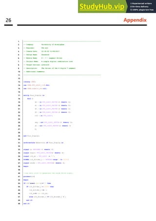
This report is about the Advance Digital Design Assignment. This assignment is aimed at using XILINX ISE TM
software and VHDL language to design a simple digital combination lock and running the design on the Nexys 3
TM Board (Figure 1) [1]. This board is a complete, ready-to-use digital circuit development platform based on the
Xilinx Spartan-6 LX16 FPGA. The simple digital combination lock is a lock which can be open via entering the
password. In this assignment, the lock is required to design as a design as a digital password checker. The
password can be reset, and the super administrator password is required before the reset process. And the
error password can be showed on the 7-segment display. While enter or reset the initial password, maximum 10
digits with the flexible digits setting is allowable in the process.
Adept
USB
Port
Power
Switch
USB HID
Host
Port
Power
Jack
JTAG
Header
MODE
Jumper
Power
Good
LED
Done
LED
Rese
t
Button
Power Select
Jumpe
r
LED
s
Slide
switch
Push
button
7-seg
Display
UART
Ethernet
Pmod
Connector
s
VHD
C
Conncector
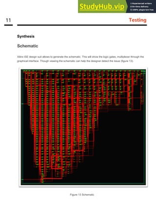
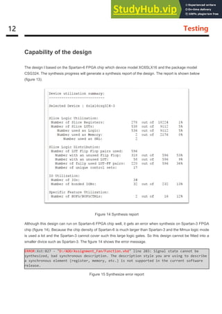
Figure 1
VGA Port](https://image.slidesharecdn.com/asimpledigitalcombinationlockadvancedigitaldesign-230806143836-138a8229/85/A-Simple-Digital-Combination-Lock-ADVANCE-DIGITAL-DESIGN-2-320.jpg)
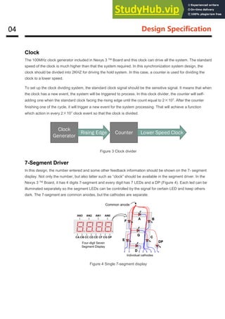
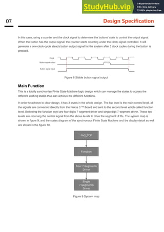
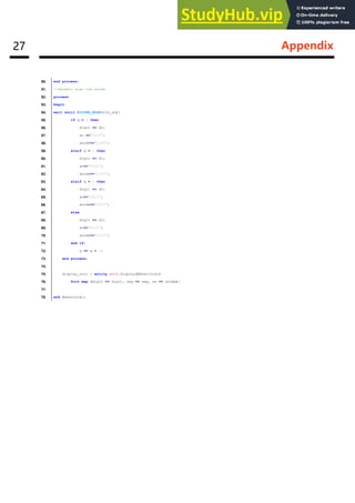
![06 Design Specification
As the Figure 5 showing above, there are four-7-segment display on the Nexys3 board and these four LED
display are common anode. The principle of 4-digit driver is to continuously refresh and repeat the display from
the first to the fourth bit (as the signal diagram shown in figure 6), and when the frequency of the scroll refresh
is higher than 45Hz, the human eyes will not detect the flash of the display and the four-digit number will be
displayed bright and continuous illumination. Since the display is a common anode, the digit display will be
achieved by controlling the cathode.
As the clock divider designed before, the same logic can be used in this four-7-segment display. However, the
clock frequency for the display is lower than that used in the main process. In the four-7-segment display driver,
the frequency is 1KHz.
De-bounce
Because of the structure and the material of the button, when the button pressed for a moment, it cannot output
a steady signal, but a jitter of the electrical frequency of the unstable signal [2]. As a result, the entire system
will be wrong when judging the button state. For example, just press the button once, the system recognizes the
press two times button, this will cause the entire system to input unstable. Therefore, the button's dithering
design is necessary.
Figure 7 Unstable button signal
AN1
AN2
AN3
AN4
Cathodes Digit0
Refresh period
= 1ms to16ms
Digit period
= Refresh/ 4
Digit1 Digit2 Digit3
Press State
Buttons signal output
Unstable signal Unstable signal
Figure 6 Reflash display signals](https://image.slidesharecdn.com/asimpledigitalcombinationlockadvancedigitaldesign-230806143836-138a8229/85/A-Simple-Digital-Combination-Lock-ADVANCE-DIGITAL-DESIGN-9-320.jpg)

![14 References
References
[1] Nexys3 TM Board Reference Manual 2013 Digilent.
[2] VHDL Code for Debounce Circuit in FPGA:
http://allaboutfpga.com/vhdl-code-for-debounce-circuit-in-fpga/](https://image.slidesharecdn.com/asimpledigitalcombinationlockadvancedigitaldesign-230806143836-138a8229/85/A-Simple-Digital-Combination-Lock-ADVANCE-DIGITAL-DESIGN-17-320.jpg)

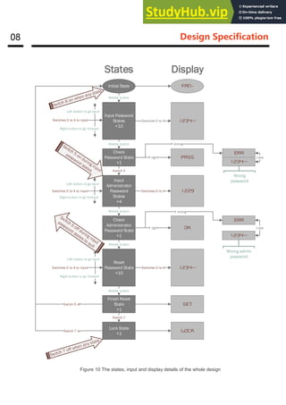
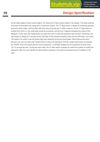
This document describes the design of a simple digital combination lock using VHDL and the Nexys 3 development board. It includes a requirement specification outlining the key functions, such as entering a password of up to 10 digits and resetting the password with an administrator code. The design specification explains the clock divider, 7-segment display drivers, and finite state machine logic. Simulation results are shown for the 7-segment displays. Testing involved synthesis, generating a schematic, and checking the design capabilities. The conclusion reflects on lessons learned about VHDL design and improvements that could be made to the lock functionality.