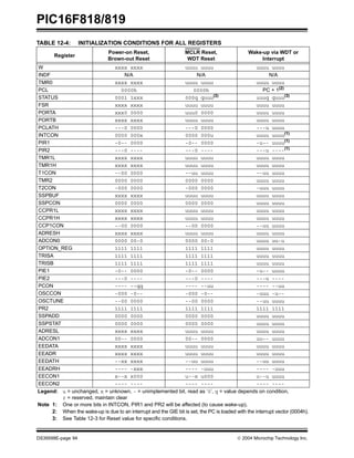
The document describes the PIC16F818/819 microcontrollers. It provides an overview of their features such as different oscillator configurations, I/O ports, timers, analog-to-digital converter, and synchronous serial port. The devices differ in memory sizes, with the PIC16F819 having more program flash and data memory. The document contains detailed specifications and electrical characteristics of the microcontrollers.


![PIC16F818/819
DS39598E-page 68 2004 Microchip Technology Inc.
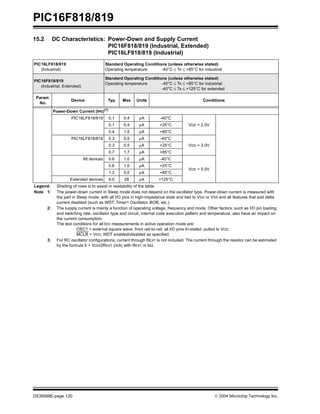
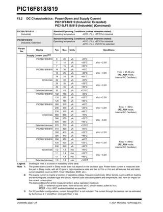
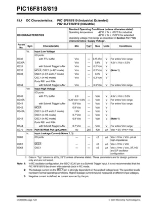
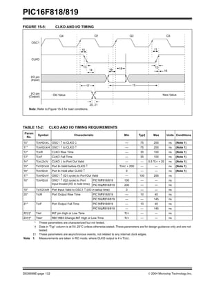
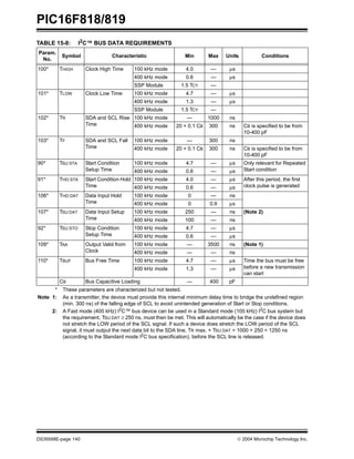
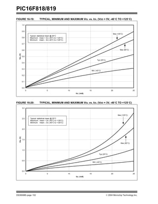
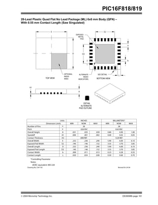
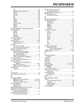
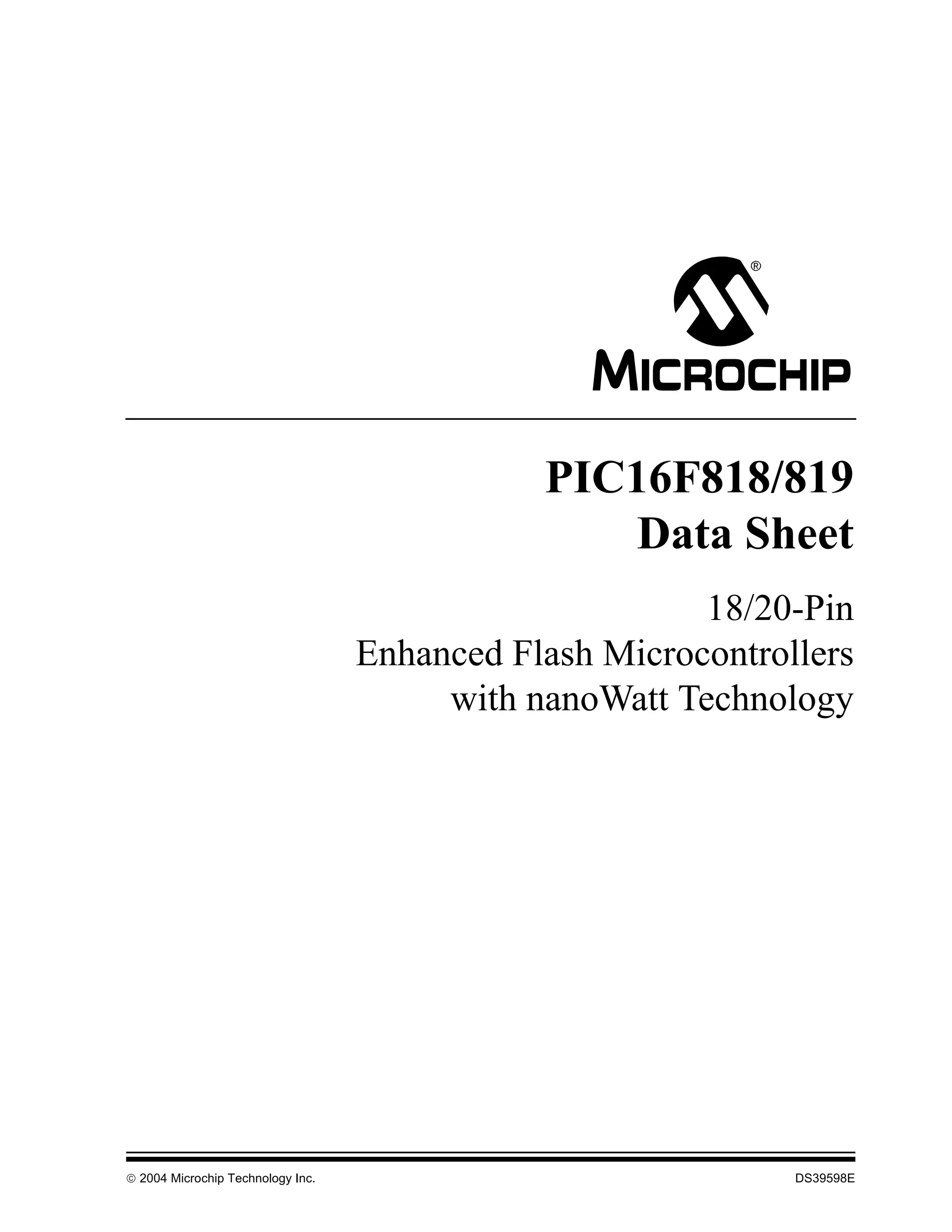
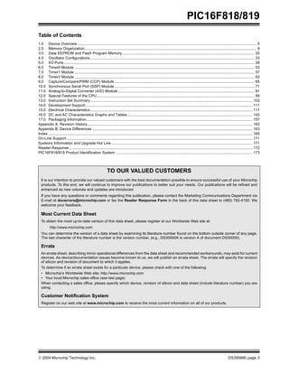
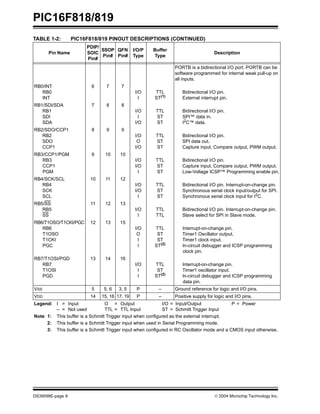
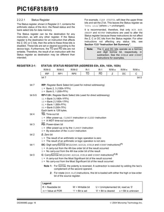
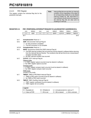
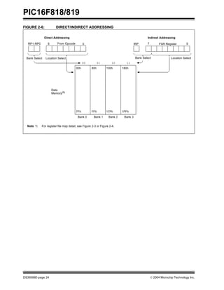
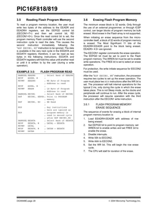
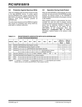
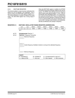
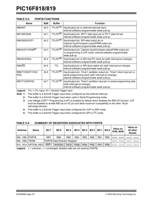
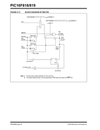
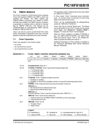
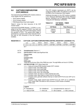
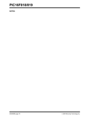
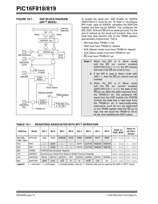
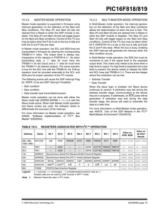
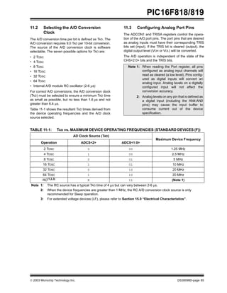
9.3 PWM Mode
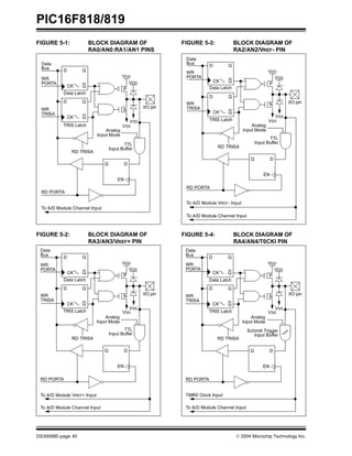
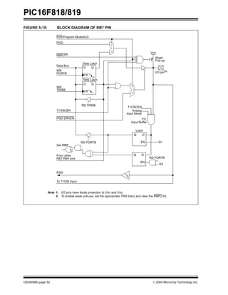
In Pulse-Width Modulation (PWM) mode, the CCP1 pin
produces up to a 10-bit resolution PWM output. Since
the CCP1 pin is multiplexed with the PORTB data latch,
the TRISB<x> bit must be cleared to make the CCP1
pin an output.
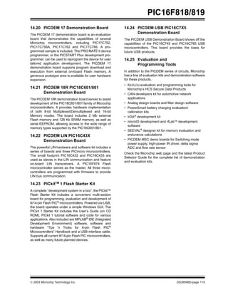
Figure 9-3 shows a simplified block diagram of the
CCP module in PWM mode.
For a step by step procedure on how to set up the CCP
module for PWM operation, see Section 9.3.3 “Setup
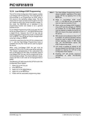
for PWM Operation”.
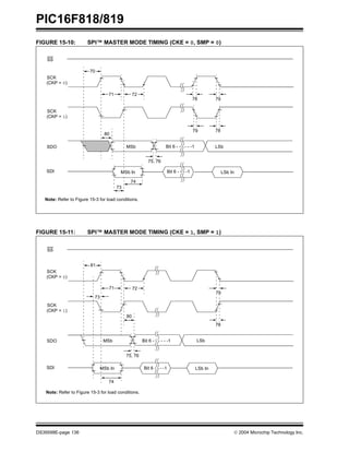
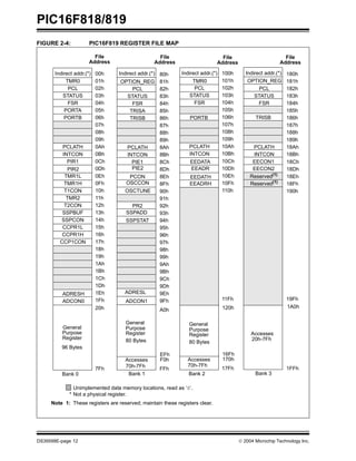
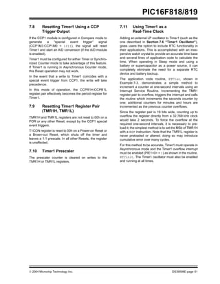
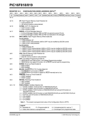
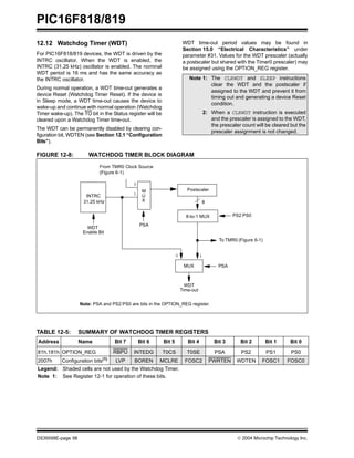
FIGURE 9-3: SIMPLIFIED PWM BLOCK
DIAGRAM
A PWM output (Figure 9-4) has a time base (period)
and a time that the output stays high (duty cycle). The
frequency of the PWM is the inverse of the period
(1/period).
FIGURE 9-4: PWM OUTPUT
9.3.1 PWM PERIOD
The PWM period is specified by writing to the PR2
register. The PWM period can be calculated using the
following formula.
EQUATION 9-1:
PWM frequency is defined as 1/[PWM period].
When TMR2 is equal to PR2, the following three events
occur on the next increment cycle:
• TMR2 is cleared
• The CCP1 pin is set (exception: if PWM duty
cycle = 0%, the CCP1 pin will not be set)
• The PWM duty cycle is latched from CCPR1L into
CCPR1H
9.3.2 PWM DUTY CYCLE
The PWM duty cycle is specified by writing to the
CCPR1L register and to the CCP1CON<5:4> bits. Up
to 10-bit resolution is available. The CCPR1L contains
the eight MSbs and the CCP1CON<5:4> contains the
two LSbs. This 10-bit value is represented by
CCPR1L:CCP1CON<5:4>. The following equation is
used to calculate the PWM duty cycle in time.
EQUATION 9-2:
CCPR1L and CCP1CON<5:4> can be written to at any
time but the duty cycle value is not latched into
CCPR1H until after a match between PR2 and TMR2
occurs (i.e., the period is complete). In PWM mode,
CCPR1H is a read-only register.
The CCPR1H register and a 2-bit internal latch are
used to double-buffer the PWM duty cycle. This
double-buffering is essential for glitchless PWM
operation.
When the CCPR1H and 2-bit latch match TMR2,
concatenated with an internal 2-bit Q clock or 2 bits of
the TMR2 prescaler, the CCP1 pin is cleared.
Note: Clearing the CCP1CON register will force
the CCP1 PWM output latch to the default
low level. This is not the PORTB I/O data
latch.
CCPR1L
CCPR1H (Slave)
Comparator
TMR2
Comparator
PR2
(Note 1)
R Q
S
Duty Cycle Registers
CCP1CON<5:4>
Clear Timer,
CCP1 pin and
latch D.C.
TRISB<x>
CCP1 pin
Note 1: 8-bit timer is concatenated with 2-bit internal Q clock
or 2 bits of the prescaler to create 10-bit time base.
Period
Duty Cycle
TMR2 = PR2
TMR2 = Duty Cycle
TMR2 = PR2
Note: The Timer2 postscaler (see Section 8.0
“Timer2 Module”) is not used in the
determination of the PWM frequency. The
postscaler could be used to have a servo
update rate at a different frequency than
the PWM output.
PWM Period = [(PR2) + 1] • 4 • TOSC •
(TMR2 Prescale Value)
PWM Duty Cycle = (CCPR1L:CCP1CON<5:4>) •
TOSC • (TMR2 Prescale Value)](https://image.slidesharecdn.com/819datasheet-211115080054/85/819-data-sheet-70-320.jpg)
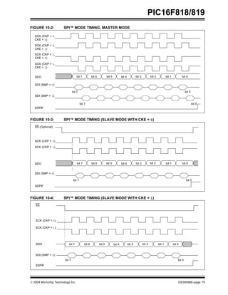
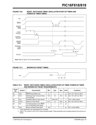
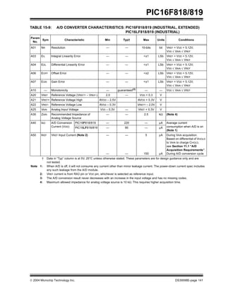
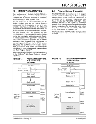
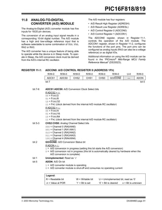
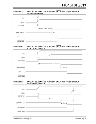
![PIC16F818/819
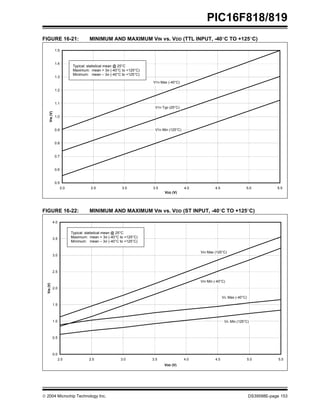
DS39598E-page 76 2004 Microchip Technology Inc.
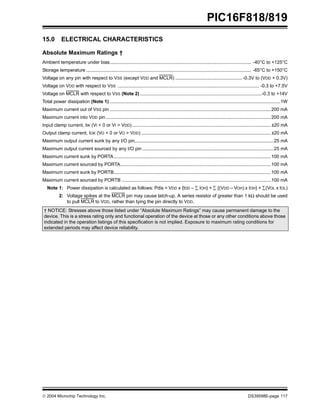
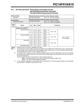
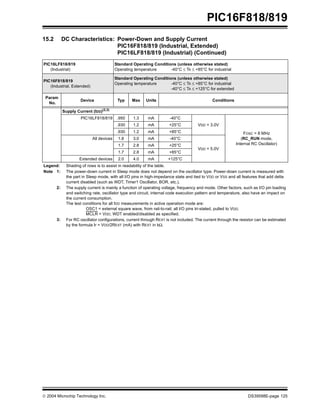
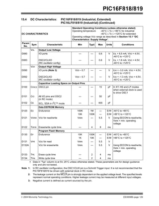
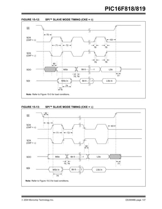
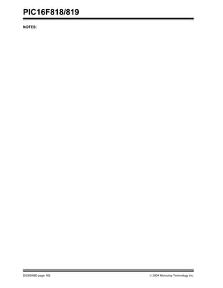
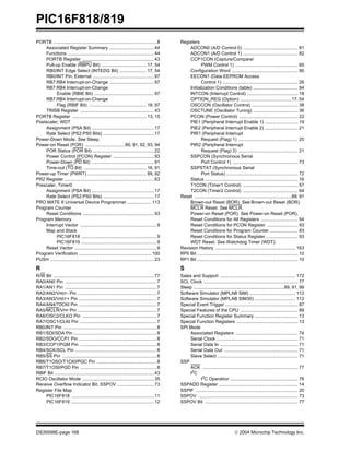
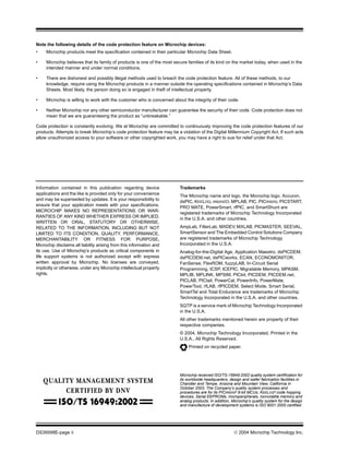
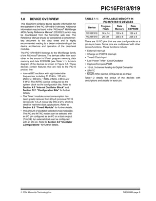
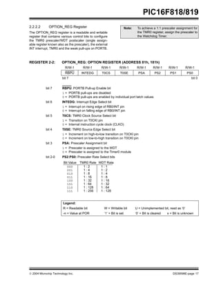
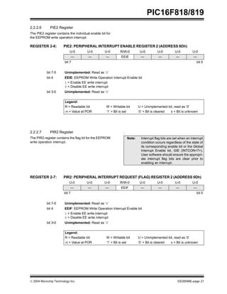
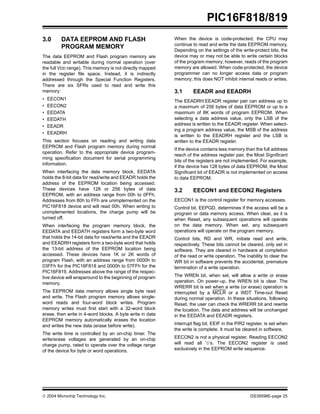
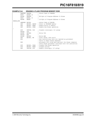
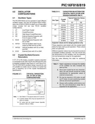
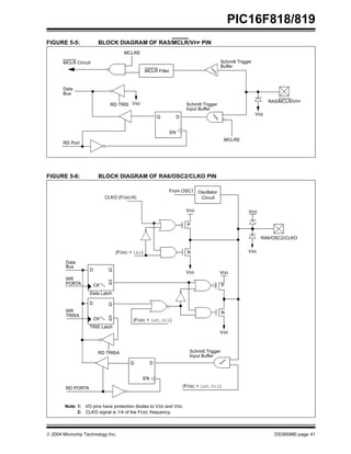
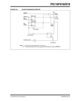
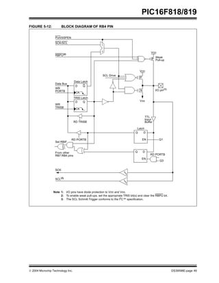
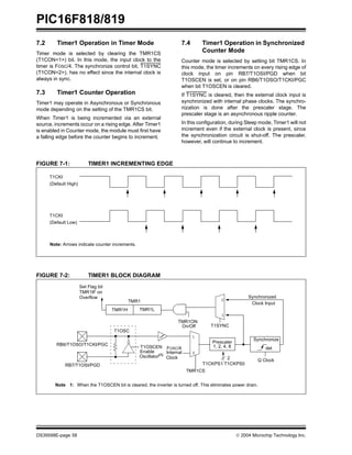
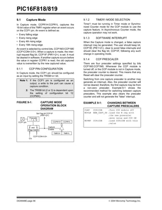
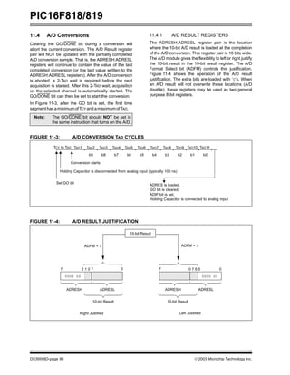
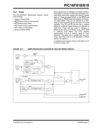
10.3 SSP I2
C Mode Operation
The SSP module in I2
C mode fully implements all slave
functions, except general call support and provides
interrupts on Start and Stop bits in hardware to facilitate
firmware implementations of the master functions. The
SSP module implements the standard mode
specifications, as well as 7-bit and 10-bit addressing.
Two pins are used for data transfer. These are the
RB4/SCK/SCL pin, which is the clock (SCL) and the
RB1/SDI/SDA pin, which is the data (SDA). The user
must configure these pins as inputs or outputs through
the TRISB<4,1> bits.
To ensure proper communication of the I2
C Slave mode,
the TRIS bits (TRISx [SDA, SCL]) corresponding to the
I2
C pins must be set to ‘1’. If any TRIS bits (TRISx<7:0>)
of the port containing the I2
C pins (PORTx [SDA, SCL])
are changed in software during I2
C communication
using a Read-Modify-Write instruction (BSF, BCF), then
the I2
C mode may stop functioning properly and I2
C
communication may suspend. Do not change any of the
TRISx bits (TRIS bits of the port containing the I2
C pins)
using the instruction BSF or BCF during I2
C communica-
tion. If it is absolutely necessary to change the TRISx
bits during communication, the following method can be
used:
EXAMPLE 10-1:
The SSP module functions are enabled by setting SSP
Enable bit, SSPEN (SSPCON<5>).
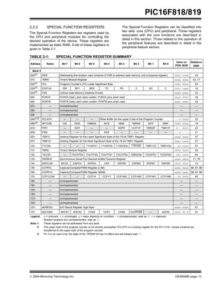
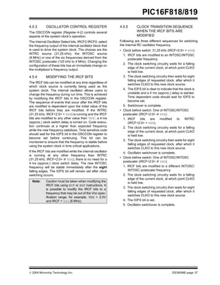
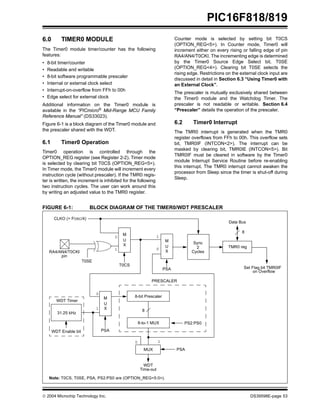
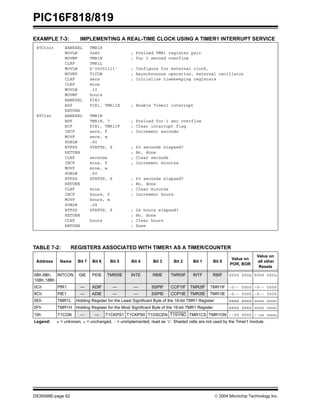
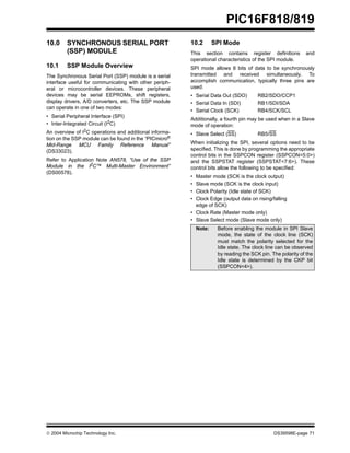
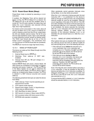
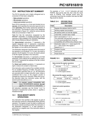
FIGURE 10-5: SSP BLOCK DIAGRAM
(I2
C™ MODE)
The SSP module has five registers for I2C operation:
• SSP Control Register (SSPCON)
• SSP Status Register (SSPSTAT)
• Serial Receive/Transmit Buffer (SSPBUF)
• SSP Shift Register (SSPSR) – Not directly
accessible
• SSP Address Register (SSPADD)
The SSPCON register allows control of the I2C opera-
tion. Four mode selection bits (SSPCON<3:0>) allow
one of the following I2C modes to be selected:
• I2C Slave mode (7-bit address)
• I2
C Slave mode (10-bit address)
• I2C Slave mode (7-bit address) with Start and
Stop bit interrupts enabled to support Firmware
Master mode
• I2
C Slave mode (10-bit address) with Start and
Stop bit interrupts enabled to support Firmware
Master mode
• I2C Firmware Controlled Master mode with Start
and Stop bit interrupts enabled, slave is Idle
Selection of any I2C mode, with the SSPEN bit set,
forces the SCL and SDA pins to be open-drain,
provided these pins are programmed to inputs by
setting the appropriate TRISB bits. Pull-up resistors
must be provided externally to the SCL and SDA pins
for proper operation of the I2C module.
Additional information on SSP I2C operation may be
found in the “PICmicro®
Mid-Range MCU Family
Reference Manual” (DS33023).
MOVF TRISC, W ; Example for an 18-pin part such as the PIC16F818/819
IORLW 0x18 ; Ensures <4:3> bits are ‘11’
ANDLW B’11111001’ ; Sets <2:1> as output, but will not alter other bits
; User can use their own logic here, such as IORLW, XORLW and ANDLW
MOVWF TRISC
Read Write
SSPSR Reg
Match Detect
SSPADD Reg
Start and
Stop Bit Detect
SSPBUF Reg
Internal
Data Bus
Addr Match
Set, Reset
S, P Bits
(SSPSTAT Reg)
RB4/SCK/
RB1/
Shift
Clock
MSb
SDI/
LSb
SDA
SCL](https://image.slidesharecdn.com/819datasheet-211115080054/85/819-data-sheet-78-320.jpg)
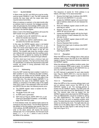

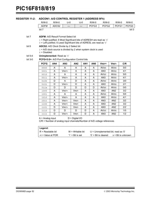
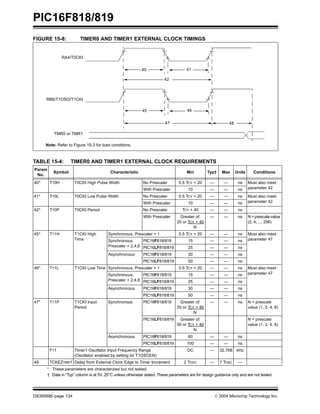
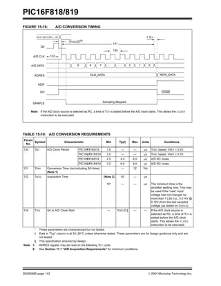
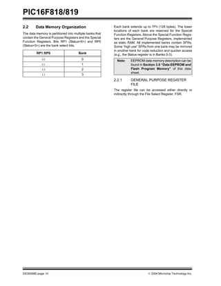
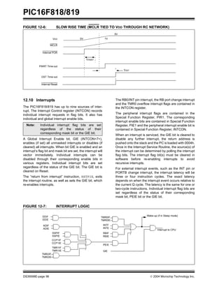
![PIC16F818/819
DS39598D-page 84 2003 Microchip Technology Inc.
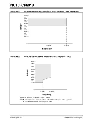
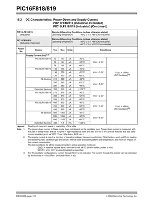
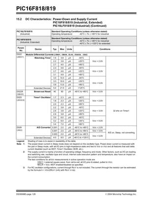
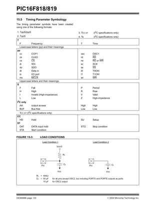
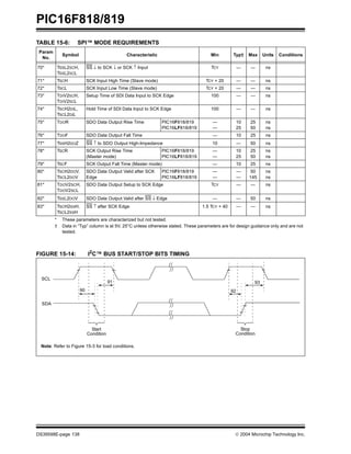
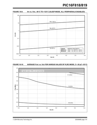
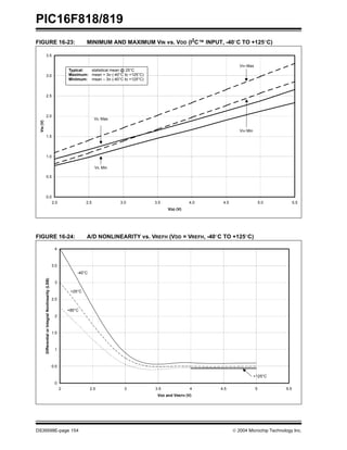
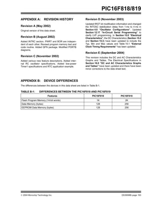
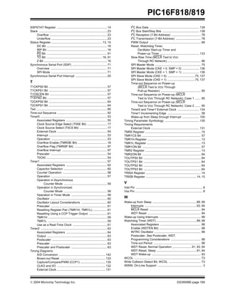
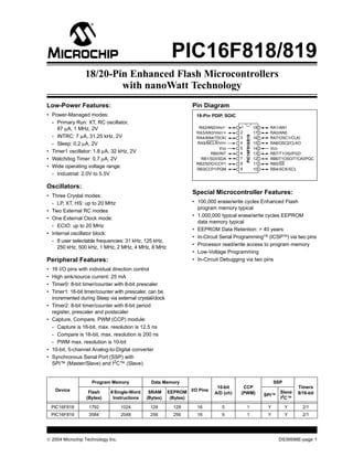
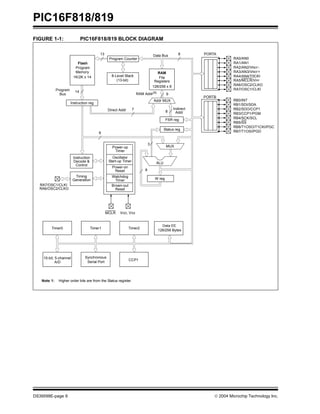
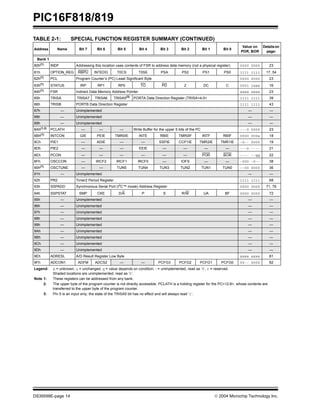
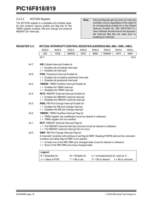
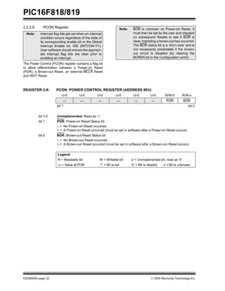
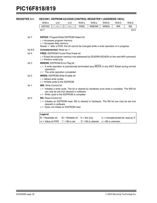
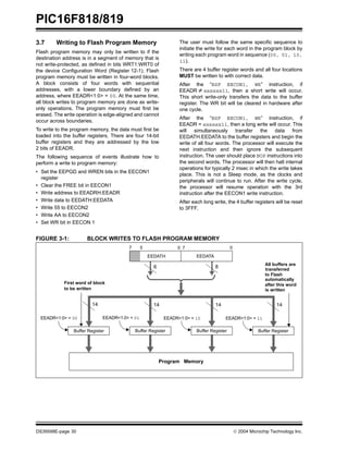
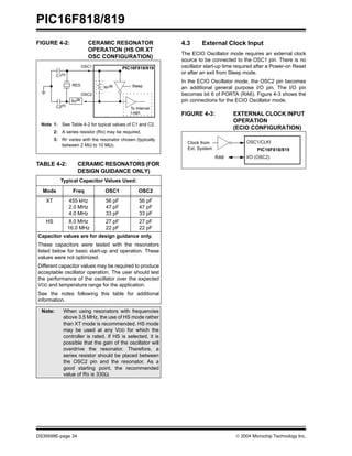
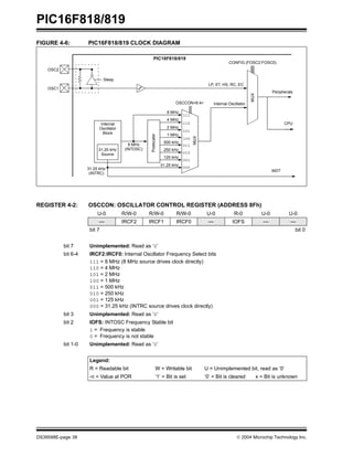
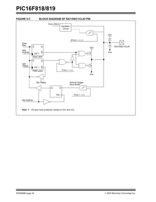
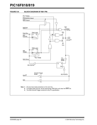
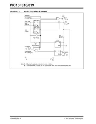
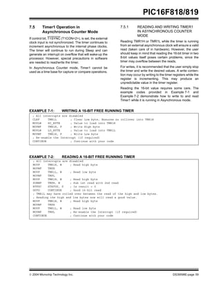
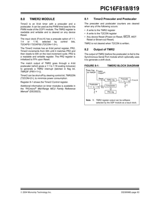
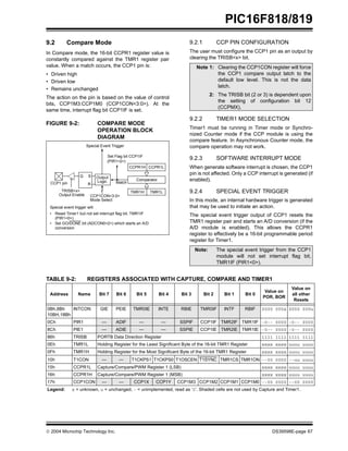
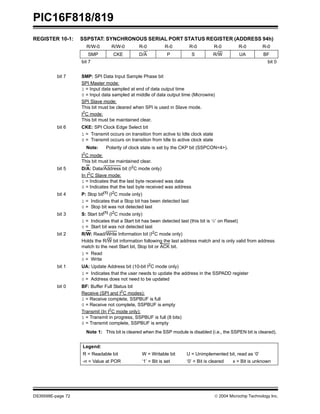
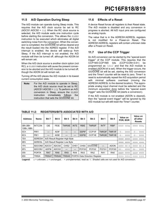
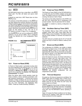
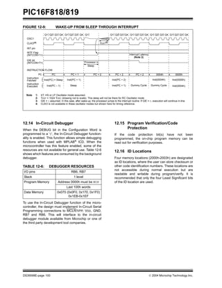
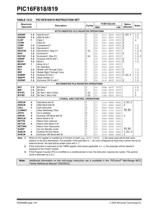
11.1 A/D Acquisition Requirements
For the A/D converter to meet its specified accuracy,
the charge holding capacitor (CHOLD) must be allowed
to fully charge to the input channel voltage level. The
analog input model is shown in Figure 11-2. The source
impedance (RS) and the internal sampling switch (RSS)
impedance directly affect the time required to charge
the capacitor CHOLD. The sampling switch (RSS)
impedance varies over the device voltage (VDD), see
Figure 11-2. The maximum recommended imped-
ance for analog sources is 2.5 kΩ. As the impedance
is decreased, the acquisition time may be decreased.
After the analog input channel is selected (changed),
this acquisition must be done before the conversion
can be started.
To calculate the minimum acquisition time,
Equation 11-1 may be used. This equation assumes
that 1/2 LSb error is used (1024 steps for the A/D). The
1/2 LSb error is the maximum error allowed for the A/D
to meet its specified resolution.
To calculate the minimum acquisition time, TACQ, see
the “PICmicro®
Mid-Range MCU Family Reference
Manual” (DS33023).
EQUATION 11-1: ACQUISITION TIME
FIGURE 11-2: ANALOG INPUT MODEL
TACQ
TC
TACQ
=
=
=
=
=
=
=
=
Amplifier Settling Time + Hold Capacitor Charging Time + Temperature Coefficient
TAMP + TC + TCOFF
2 µs + TC + [(Temperature – 25°C)(0.05 µs/°C)]
CHOLD (RIC + RSS + RS) In(1/2047)
-120 pF (1 kΩ + 7 kΩ + 10 kΩ) In(0.0004885)
16.47 µs
2 µs + 16.47 µs + [(50°C – 25°C)(0.05 µs/°C)
19.72 µs
Note 1: The reference voltage (VREF) has no effect on the equation since it cancels itself out.
2: The charge holding capacitor (CHOLD) is not discharged after each conversion.
3: The maximum recommended impedance for analog sources is 10 kΩ. This is required to meet the pin
leakage specification.
4: After a conversion has completed, a 2.0 TAD delay must complete before acquisition can begin again.
During this time, the holding capacitor is not connected to the selected A/D input channel.
CPIN
VA
RS ANx
5 pF
VDD
VT = 0.6V
VT = 0.6V
ILEAKAGE
RIC ≤ 1K
Sampling
Switch
SS RSS
CHOLD
= DAC Capacitance
VSS
6V
Sampling Switch
5V
4V
3V
2V
5 6 7 8 9 10 11
(kΩ)
VDD
= 120 pF
± 500 nA
Legend: CPIN
VT
ILEAKAGE
RIC
SS
CHOLD
= input capacitance
= threshold voltage
= leakage current at the pin due to
= interconnect resistance
= sampling switch
= sample/hold capacitance (from DAC)
various junctions](https://image.slidesharecdn.com/819datasheet-211115080054/85/819-data-sheet-86-320.jpg)

![ 2004 Microchip Technology Inc. DS39598E-page 105
PIC16F818/819
13.2 Instruction Descriptions
ADDLW Add Literal and W
Syntax: [ label ] ADDLW k
Operands: 0 ≤ k ≤ 255
Operation: (W) + k → (W)
Status Affected: C, DC, Z
Description: The contents of the W register
are added to the eight-bit literal ‘k’
and the result is placed in the W
register.
ADDWF Add W and f
Syntax: [ label ] ADDWF f,d
Operands: 0 ≤ f ≤ 127
d ∈ [0,1]
Operation: (W) + (f) → (destination)
Status Affected: C, DC, Z
Description: Add the contents of the W register
with register ‘f’. If ‘d’ = 0, the result
is stored in the W register. If
‘d’ = 1, the result is stored back in
register ‘f’.
ANDLW AND Literal with W
Syntax: [ label ] ANDLW k
Operands: 0 ≤ k ≤ 255
Operation: (W) .AND. (k) → (W)
Status Affected: Z
Description: The contents of W register are
ANDed with the eight-bit literal ‘k’.
The result is placed in the W
register.
ANDWF AND W with f
Syntax: [ label ] ANDWF f,d
Operands: 0 ≤ f ≤ 127
d ∈ [0,1]
Operation: (W) .AND. (f) → (destination)
Status Affected: Z
Description: AND the W register with register
‘f’. If ‘d’ = 0, the result is stored in
the W register. If ‘d’ = 1, the result
is stored back in register ‘f’.
BCF Bit Clear f
Syntax: [ label ] BCF f,b
Operands: 0 ≤ f ≤ 127
0 ≤ b ≤ 7
Operation: 0 → (f<b>)
Status Affected: None
Description: Bit ‘b’ in register ‘f’ is cleared.
BSF Bit Set f
Syntax: [ label ] BSF f,b
Operands: 0 ≤ f ≤ 127
0 ≤ b ≤ 7
Operation: 1 → (f<b>)
Status Affected: None
Description: Bit ‘b’ in register ‘f’ is set.](https://image.slidesharecdn.com/819datasheet-211115080054/85/819-data-sheet-107-320.jpg)
![PIC16F818/819
DS39598E-page 106 2004 Microchip Technology Inc.
BTFSS Bit Test f, Skip if Set
Syntax: [ label ] BTFSS f,b
Operands: 0 ≤ f ≤ 127
0 ≤ b < 7
Operation: skip if (f<b>) = 1
Status Affected: None
Description: If bit ‘b’ in register ‘f’ = 0, the next
instruction is executed.
If bit ‘b’ = 1, then the next
instruction is discarded and a NOP
is executed instead, making this a
2 TCY instruction.
BTFSC Bit Test, Skip if Clear
Syntax: [ label ] BTFSC f,b
Operands: 0 ≤ f ≤ 127
0 ≤ b ≤ 7
Operation: skip if (f<b>) = 0
Status Affected: None
Description: If bit ‘b’ in register ‘f’ = 1, the next
instruction is executed.
If bit ‘b’ in register ‘f’ = 0, the next
instruction is discarded and a NOP
is executed instead, making this a
2 TCY instruction.
CALL Call Subroutine
Syntax: [ label ] CALL k
Operands: 0 ≤ k ≤ 2047
Operation: (PC) + 1 → TOS,
k → PC<10:0>,
(PCLATH<4:3>) → PC<12:11>
Status Affected: None
Description: Call subroutine. First, return
address (PC + 1) is pushed onto
the stack. The eleven-bit
immediate address is loaded into
PC bits<10:0>. The upper bits of
the PC are loaded from PCLATH.
CALL is a two-cycle instruction.
CLRF Clear f
Syntax: [ label ] CLRF f
Operands: 0 ≤ f ≤ 127
Operation: 00h → (f)
1 → Z
Status Affected: Z
Description: The contents of register ‘f’ are
cleared and the Z bit is set.
CLRW Clear W
Syntax: [ label ] CLRW
Operands: None
Operation: 00h → (W)
1 → Z
Status Affected: Z
Description: W register is cleared. Zero bit (Z)
is set.
CLRWDT Clear Watchdog Timer
Syntax: [ label ] CLRWDT
Operands: None
Operation: 00h → WDT
0 → WDT prescaler,
1 → TO
1 → PD
Status Affected: TO, PD
Description: CLRWDT instruction resets the
Watchdog Timer. It also resets the
prescaler of the WDT. Status bits
TO and PD are set.](https://image.slidesharecdn.com/819datasheet-211115080054/85/819-data-sheet-108-320.jpg)
![ 2004 Microchip Technology Inc. DS39598E-page 107
PIC16F818/819
COMF Complement f
Syntax: [ label ] COMF f,d
Operands: 0 ≤ f ≤ 127
d ∈ [0,1]
Operation: (f) → (destination)
Status Affected: Z
Description: The contents of register ‘f’ are
complemented. If ‘d’ = 0, the
result is stored in W. If ‘d’ = 1, the
result is stored back in register ‘f’.
DECF Decrement f
Syntax: [ label ] DECF f,d
Operands: 0 ≤ f ≤ 127
d ∈ [0,1]
Operation: (f) – 1 → (destination)
Status Affected: Z
Description: Decrement register ‘f’. If ‘d’ = 0,
the result is stored in the W
register. If ‘d’ = 1, the result is
stored back in register ‘f’.
DECFSZ Decrement f, Skip if 0
Syntax: [ label ] DECFSZ f,d
Operands: 0 ≤ f ≤ 127
d ∈ [0,1]
Operation: (f) – 1 → (destination);
skip if result = 0
Status Affected: None
Description: The contents of register ‘f’ are
decremented. If ‘d’ = 0, the result
is placed in the W register. If
‘d’ = 1, the result is placed back in
register ‘f’.
If the result is ‘1’, the next
instruction is executed. If the
result is ‘0’, then a NOP is
executed instead, making it a
2 TCY instruction.
GOTO Unconditional Branch
Syntax: [ label ] GOTO k
Operands: 0 ≤ k ≤ 2047
Operation: k → PC<10:0>
PCLATH<4:3> → PC<12:11>
Status Affected: None
Description: GOTO is an unconditional branch.
The eleven-bit immediate value is
loaded into PC bits<10:0>. The
upper bits of PC are loaded
from PCLATH<4:3>. GOTO is a
two-cycle instruction.
INCF Increment f
Syntax: [ label ] INCF f,d
Operands: 0 ≤ f ≤ 127
d ∈ [0,1]
Operation: (f) + 1 → (destination)
Status Affected: Z
Description: The contents of register ‘f’ are
incremented. If ‘d’ = 0, the result
is placed in the W register. If
‘d’ = 1, the result is placed back in
register ‘f’.
INCFSZ Increment f, Skip if 0
Syntax: [ label ] INCFSZ f,d
Operands: 0 ≤ f ≤ 127
d ∈ [0,1]
Operation: (f) + 1 → (destination),
skip if result = 0
Status Affected: None
Description: The contents of register ‘f’ are
incremented. If ‘d’ = 0, the result is
placed in the W register. If ‘d’ = 1,
the result is placed back in
register ‘f’.
If the result is ‘1’, the next
instruction is executed. If the
result is ‘0’, a NOP is executed
instead, making it a 2 TCY
instruction.](https://image.slidesharecdn.com/819datasheet-211115080054/85/819-data-sheet-109-320.jpg)
![PIC16F818/819
DS39598E-page 108 2004 Microchip Technology Inc.
IORLW Inclusive OR Literal with W
Syntax: [ label ] IORLW k
Operands: 0 ≤ k ≤ 255
Operation: (W) .OR. k → (W)
Status Affected: Z
Description: The contents of the W register are
ORed with the eight-bit literal ‘k’.
The result is placed in the W
register.
IORWF Inclusive OR W with f
Syntax: [ label ] IORWF f,d
Operands: 0 ≤ f ≤ 127
d ∈ [0,1]
Operation: (W) .OR. (f) → (destination)
Status Affected: Z
Description: Inclusive OR the W register with
register ‘f’. If ‘d’ = 0, the result is
placed in the W register. If ‘d’ = 1,
the result is placed back in
register ‘f’.
MOVF Move f
Syntax: [ label ] MOVF f,d
Operands: 0 ≤ f ≤ 127
d ∈ [0,1]
Operation: (f) → (destination)
Status Affected: Z
Description: The contents of register ‘f’ are
moved to a destination dependant
upon the status of ‘d’. If ‘d’ = 0,
the destination is W register. If
‘d’ = 1, the destination is file regis-
ter ‘f’ itself. ‘d’ = 1 is useful to test
a file register since status flag Z is
affected.
MOVLW Move Literal to W
Syntax: [ label ] MOVLW k
Operands: 0 ≤ k ≤ 255
Operation: k → (W)
Status Affected: None
Description: The eight-bit literal ‘k’ is loaded
into W register. The don’t cares
will assemble as ‘0’s.
MOVWF Move W to f
Syntax: [ label ] MOVWF f
Operands: 0 ≤ f ≤ 127
Operation: (W) → (f)
Status Affected: None
Description: Move data from W register to
register ‘f’.
NOP No Operation
Syntax: [ label ] NOP
Operands: None
Operation: No operation
Status Affected: None
Description: No operation.](https://image.slidesharecdn.com/819datasheet-211115080054/85/819-data-sheet-110-320.jpg)
![ 2004 Microchip Technology Inc. DS39598E-page 109
PIC16F818/819
RETFIE Return from Interrupt
Syntax: [ label ] RETFIE
Operands: None
Operation: TOS → PC,
1 → GIE
Status Affected: None
RETLW Return with Literal in W
Syntax: [ label ] RETLW k
Operands: 0 ≤ k ≤ 255
Operation: k → (W);
TOS → PC
Status Affected: None
Description: The W register is loaded with the
eight-bit literal ‘k’. The program
counter is loaded from the top of
the stack (the return address).
This is a two-cycle instruction.
RETURN Return from Subroutine
Syntax: [ label ] RETURN
Operands: None
Operation: TOS → PC
Status Affected: None
Description: Return from subroutine. The stack
is POPed and the top of the stack
(TOS) is loaded into the program
counter. This is a two-cycle
instruction.
RLF Rotate Left f through Carry
Syntax: [ label ] RLF f,d
Operands: 0 ≤ f ≤ 127
d ∈ [0,1]
Operation: See description below
Status Affected: C
Description: The contents of register ‘f’ are
rotated one bit to the left through
the Carry flag. If ‘d’ = 0, the result
is placed in the W register. If
‘d’ = 1, the result is stored back in
register ‘f’.
RRF Rotate Right f through Carry
Syntax: [ label ] RRF f,d
Operands: 0 ≤ f ≤ 127
d ∈ [0,1]
Operation: See description below
Status Affected: C
Description: The contents of register ‘f’ are
rotated one bit to the right through
the Carry flag. If ‘d’ = 0, the result
is placed in the W register. If
‘d’ = 1, the result is placed back in
register ‘f’.
SLEEP Enter Sleep mode
Syntax: [ label ] SLEEP
Operands: None
Operation: 00h → WDT,
0 → WDT prescaler,
1 → TO,
0 → PD
Status Affected: TO, PD
Description: The Power-Down status bit, PD,
is cleared. Time-out status bit,
TO, is set. Watchdog Timer and
its prescaler are cleared.
The processor is put into Sleep
mode with the oscillator stopped.
Register f
C
Register f
C](https://image.slidesharecdn.com/819datasheet-211115080054/85/819-data-sheet-111-320.jpg)
![PIC16F818/819
DS39598E-page 110 2004 Microchip Technology Inc.
SUBLW Subtract W from Literal
Syntax: [ label ] SUBLW k
Operands: 0 ≤ k ≤ 255
Operation: k – (W) → (W)
Status Affected: C, DC, Z
Description: The W register is subtracted (2’s
complement method) from the
eight-bit literal ‘k’. The result is
placed in the W register.
SUBWF Subtract W from f
Syntax: [ label ] SUBWF f,d
Operands: 0 ≤ f ≤ 127
d ∈ [0,1]
Operation: (f) – (W) → (destination)
Status Affected: C, DC, Z
Description: Subtract (2’s complement method)
W register from register ‘f’. If
‘d’ = 0, the result is stored in the W
register. If ‘d’ = 1, the result is
stored back in register ‘f’.
SWAPF Swap Nibbles in f
Syntax: [ label ] SWAPF f,d
Operands: 0 ≤ f ≤ 127
d ∈ [0,1]
Operation: (f<3:0>) → (destination<7:4>),
(f<7:4>) → (destination<3:0>)
Status Affected: None
Description: The upper and lower nibbles of
register ‘f’ are exchanged. If
‘d’ = 0, the result is placed in W
register. If ‘d’ = 1, the result is
placed in register ‘f’.
XORLW Exclusive OR Literal with W
Syntax: [ label ] XORLW k
Operands: 0 ≤ k ≤ 255
Operation: (W) .XOR. k → (W)
Status Affected: Z
Description: The contents of the W register
are XORed with the eight-bit
literal ‘k’. The result is placed in
the W register.
XORWF Exclusive OR W with f
Syntax: [ label ] XORWF f,d
Operands: 0 ≤ f ≤ 127
d ∈ [0,1]
Operation: (W) .XOR. (f) → (destination)
Status Affected: Z
Description: Exclusive OR the contents of the
W register with register ‘f’. If
‘d’ = 0, the result is stored in the
W register. If ‘d’ = 1, the result is
stored back in register ‘f’.](https://image.slidesharecdn.com/819datasheet-211115080054/85/819-data-sheet-112-320.jpg)