Downloaded 24 times


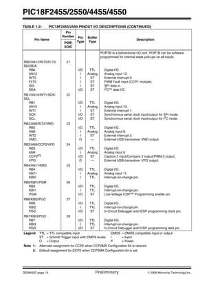


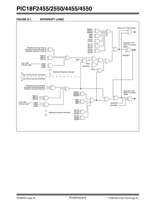
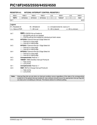
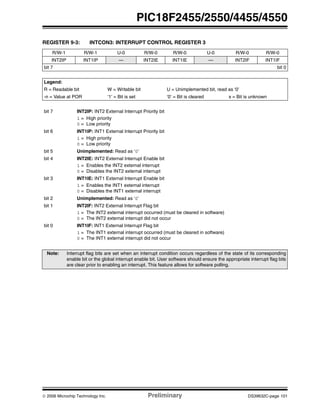
![PIC18F2455/2550/4455/4550
DS39632C-page 76 Preliminary © 2006 Microchip Technology Inc.
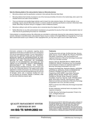
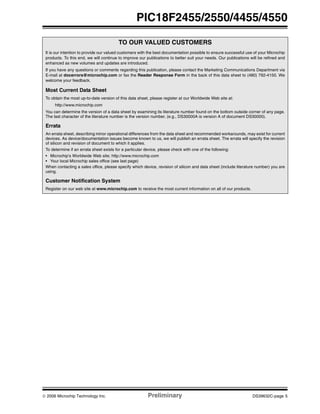
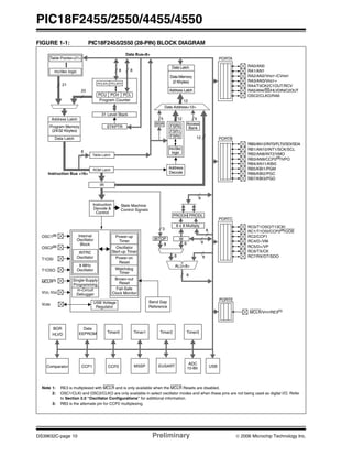
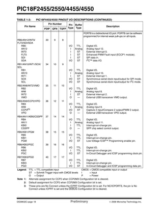
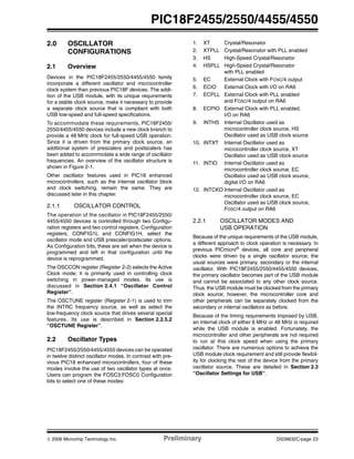
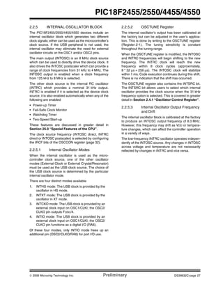
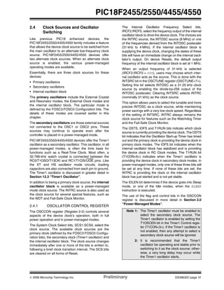
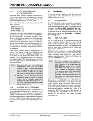
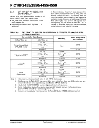
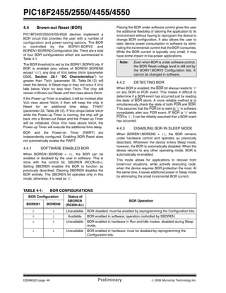
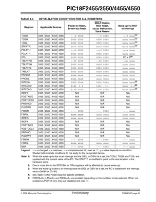
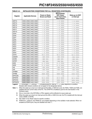
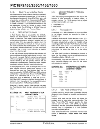
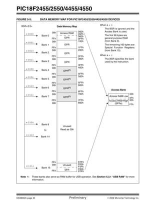
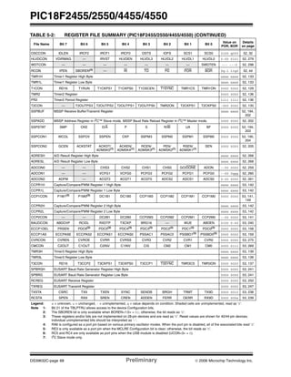
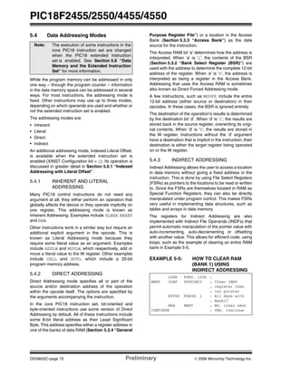
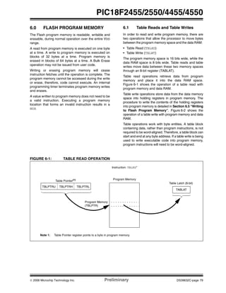
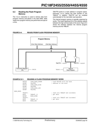
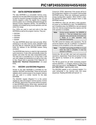
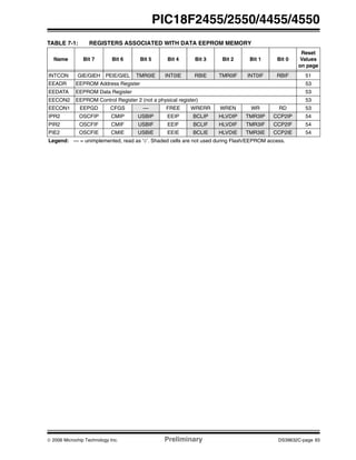
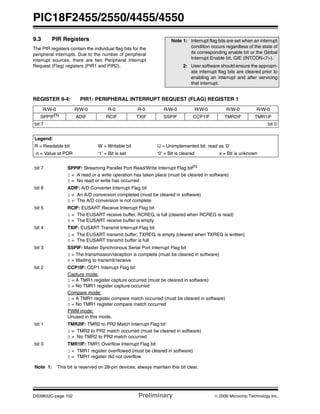
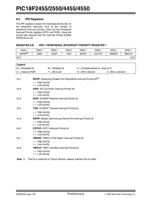
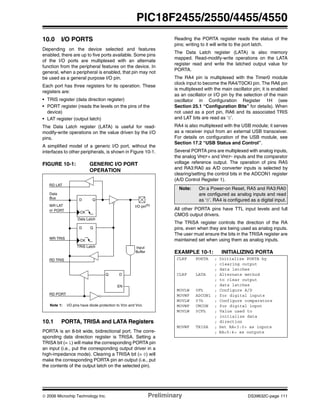
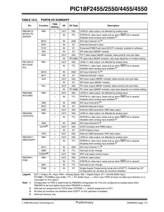
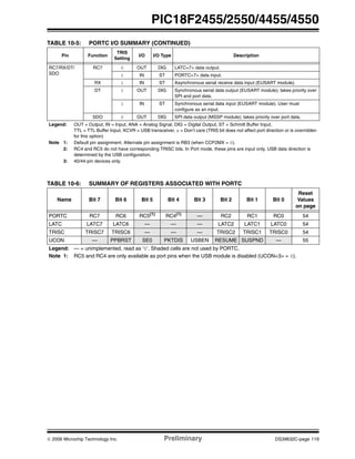
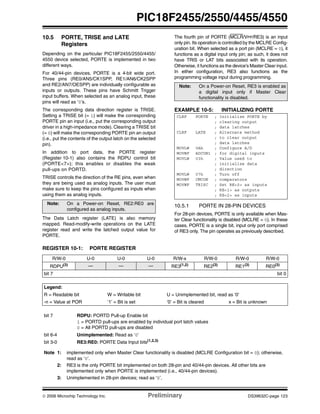
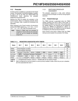
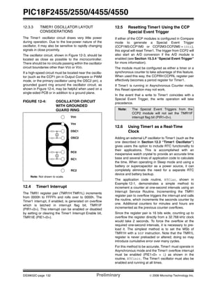
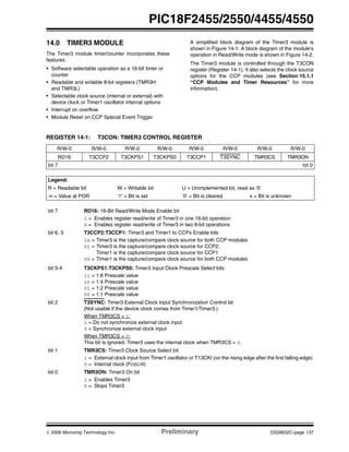
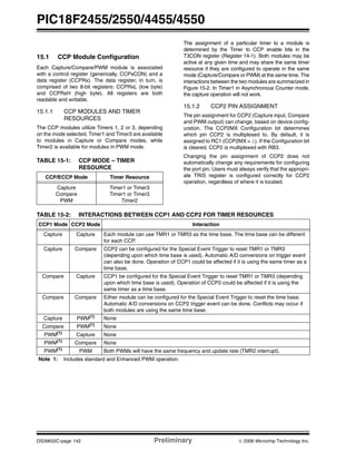
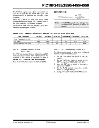
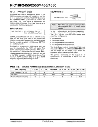
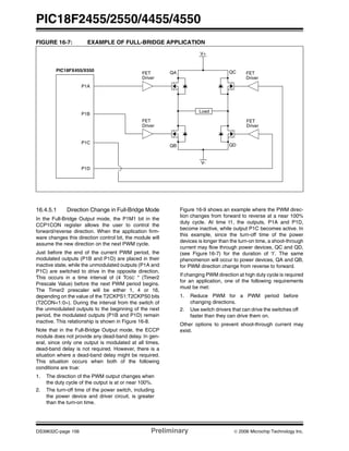
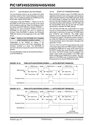
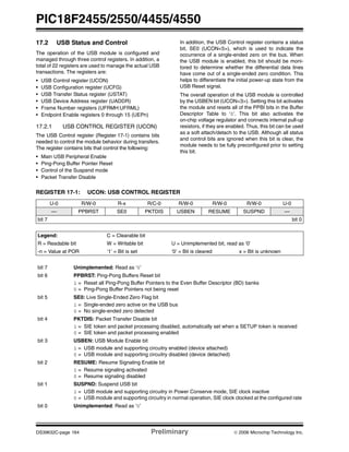
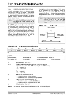
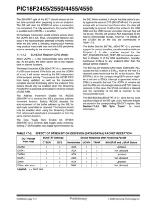
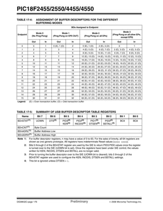
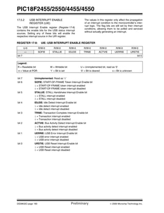
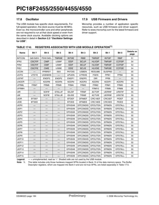
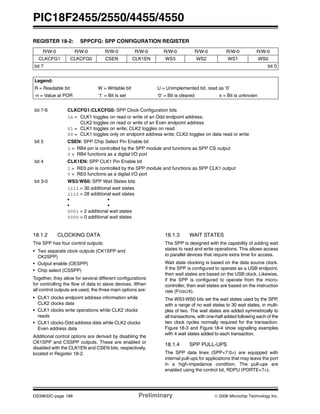
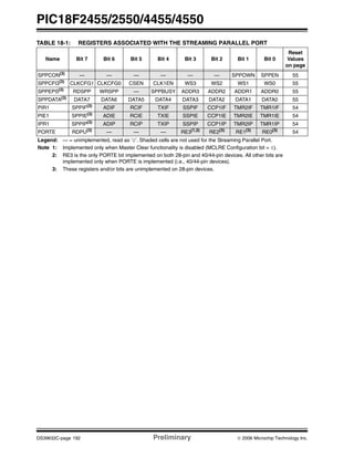
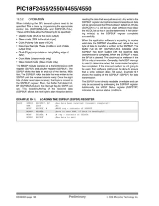
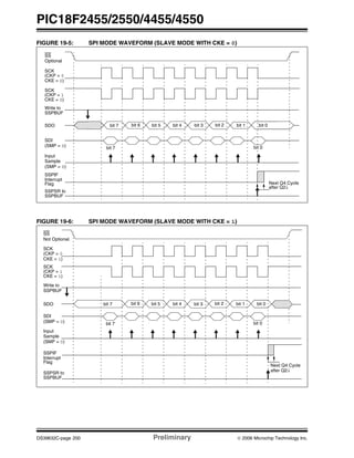
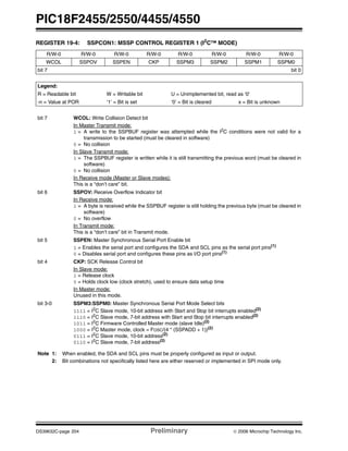
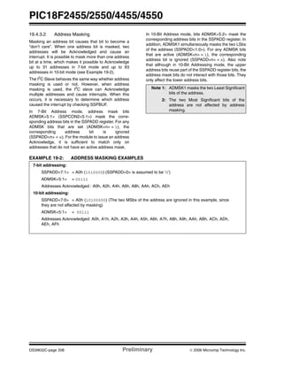
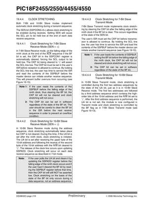
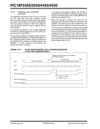
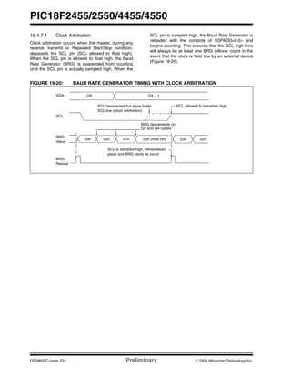
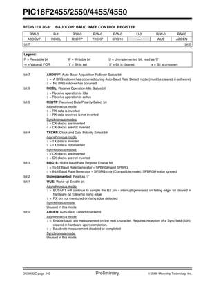
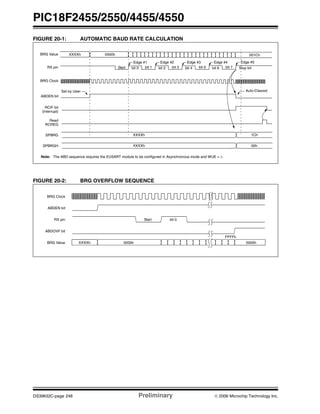
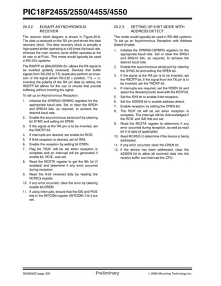
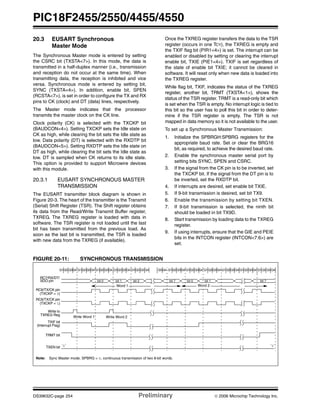
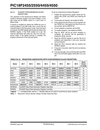
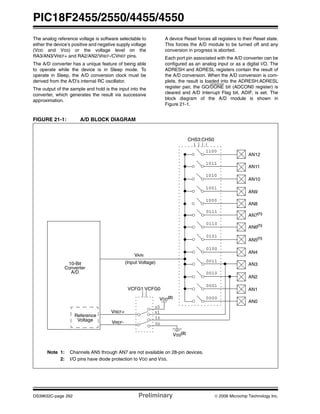
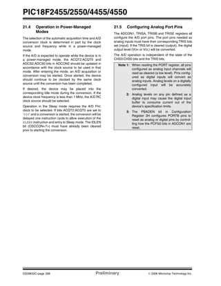
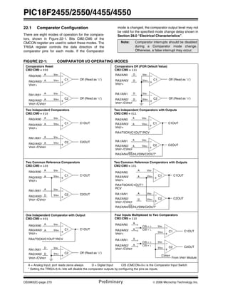
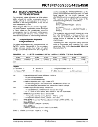
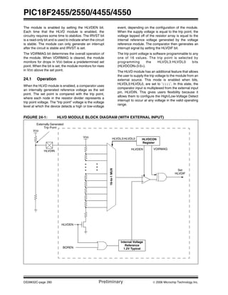
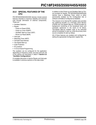
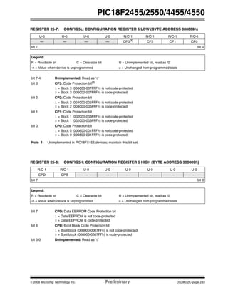
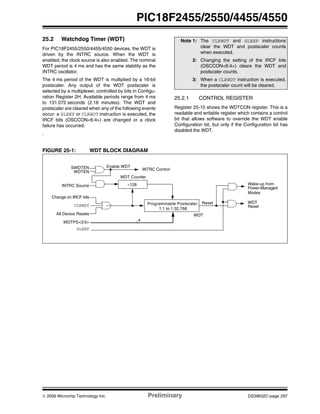
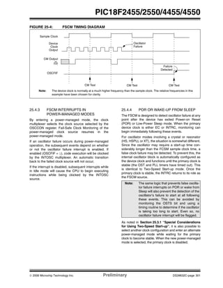
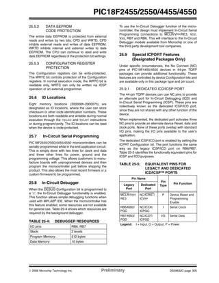
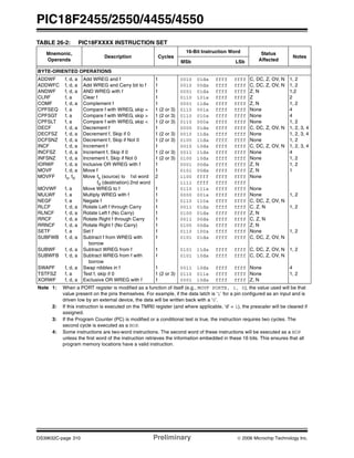
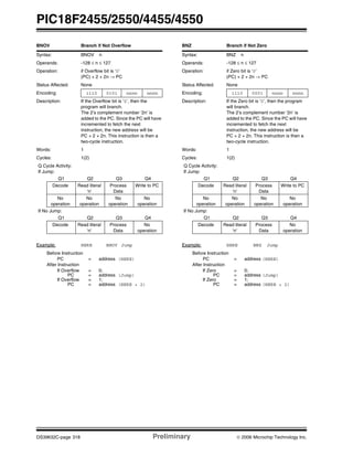
FIGURE 5-8: COMPARING ADDRESSING OPTIONS FOR BIT-ORIENTED AND
BYTE-ORIENTED INSTRUCTIONS (EXTENDED INSTRUCTION SET ENABLED)
EXAMPLE INSTRUCTION: ADDWF, f, d, a (Opcode: 0010 01da ffff ffff)
When a = 0 and f ≥ 60h:
The instruction executes in
Direct Forced mode. ‘f’ is inter-
preted as a location in the
Access RAM between 060h
and 0FFh. This is the same as
the SFRs or locations F60h to
0FFh (Bank 15) of data
memory.
Locations below 60h are not
available in this addressing
mode.
When a = 0 and f ≤ 5Fh:
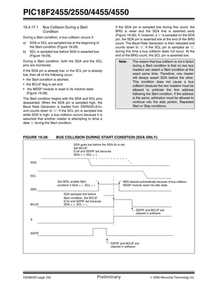
The instruction executes in
Indexed Literal Offset mode. ‘f’
is interpreted as an offset to the
address value in FSR2. The
two are added together to
obtain the address of the target
register for the instruction. The
address can be anywhere in
the data memory space.
Note that in this mode, the
correct syntax is now:
ADDWF [k], d
where ‘k’ is the same as ‘f’.
When a = 1 (all values of f):
The instruction executes in
Direct mode (also known as
Direct Long mode). ‘f’ is inter-
preted as a location in one of
the 16 banks of the data
memory space. The bank is
designated by the Bank Select
Register (BSR). The address
can be in any implemented
bank in the data memory
space.
000h
060h
100h
F00h
F60h
FFFh
Valid range
00h
60h
FFh
Data Memory
Access RAM
Bank 0
Bank 1
through
Bank 14
Bank 15
SFRs
000h
080h
100h
F00h
F60h
FFFh
Data Memory
Bank 0
Bank 1
through
Bank 14
Bank 15
SFRs
FSR2H FSR2L
ffffffff001001da
ffffffff001001da
000h
080h
100h
F00h
F60h
FFFh
Data Memory
Bank 0
Bank 1
through
Bank 14
Bank 15
SFRs
for ‘f’
BSR
00000000
080h](https://image.slidesharecdn.com/pic18f4550-140425123621-phpapp01/85/Pic18f4550-78-320.jpg)


![PIC18F2455/2550/4455/4550
DS39632C-page 146 Preliminary © 2006 Microchip Technology Inc.
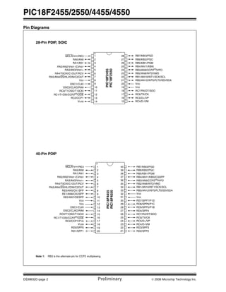
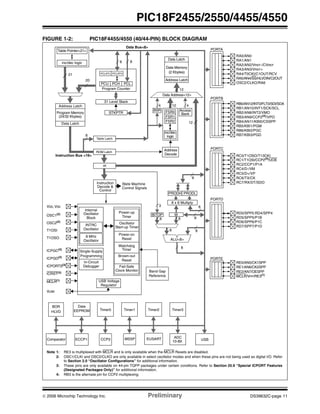
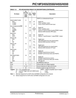
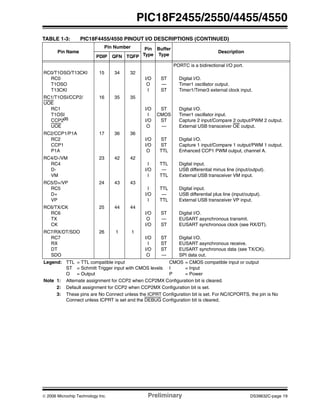
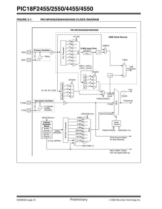
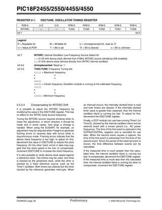
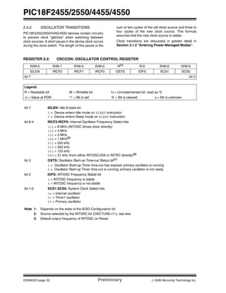
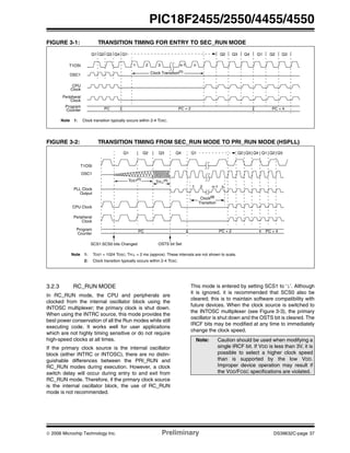
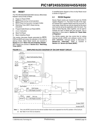
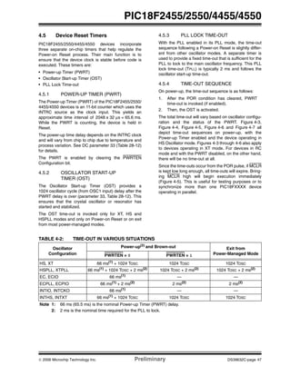
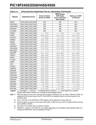
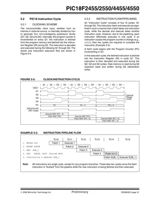
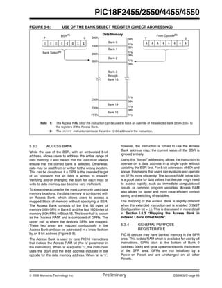
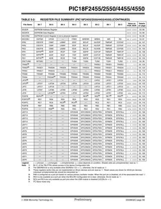
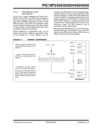
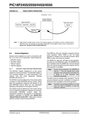
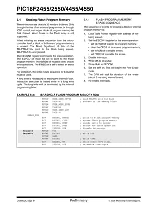
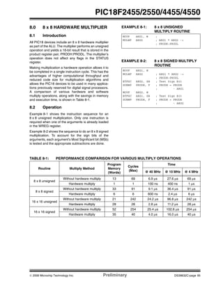
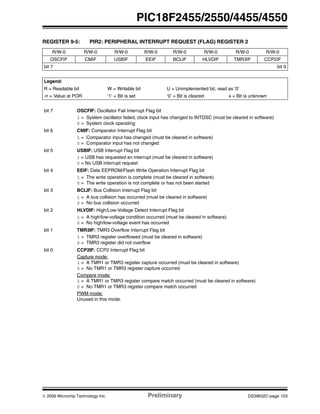
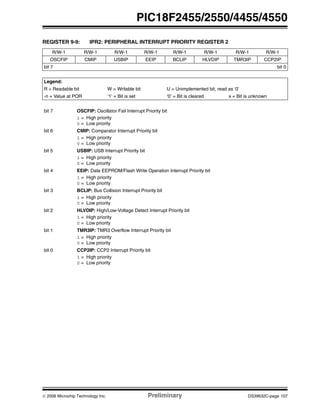
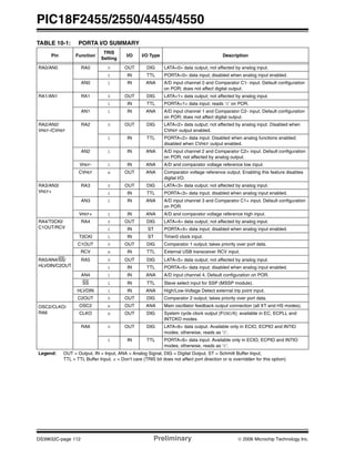
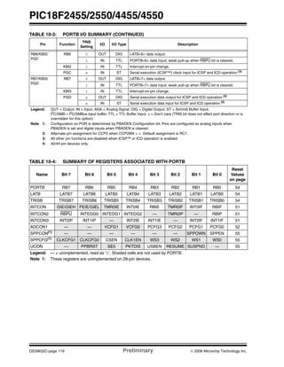
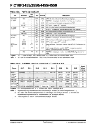
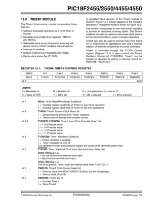
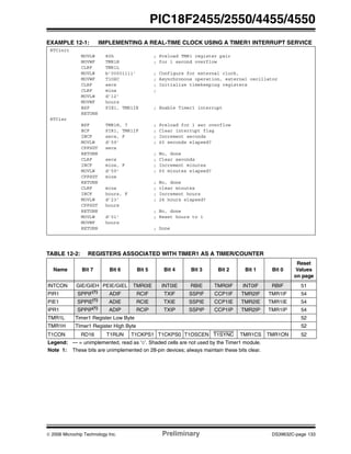
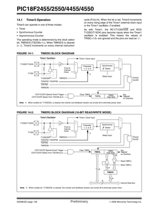
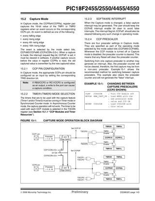
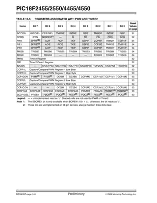
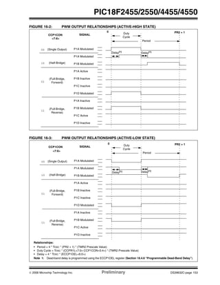
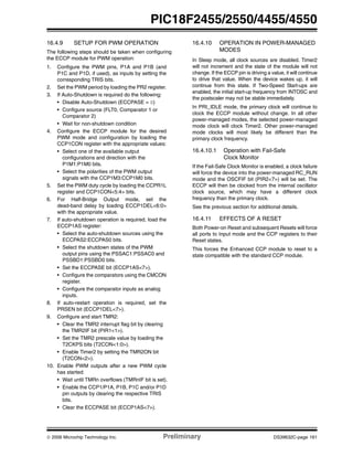
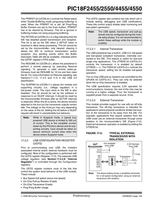
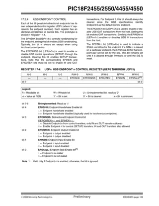
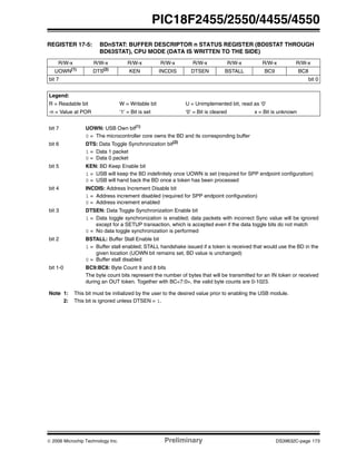
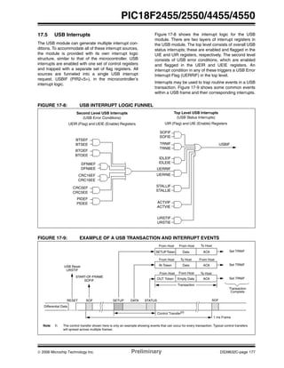
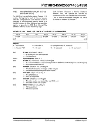
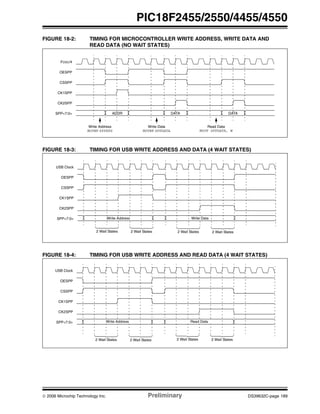
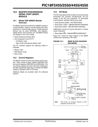
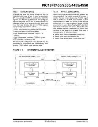
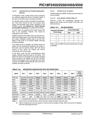
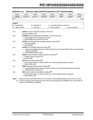
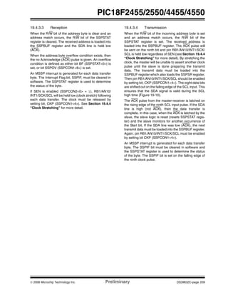
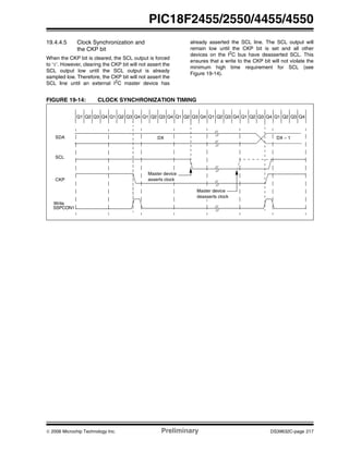
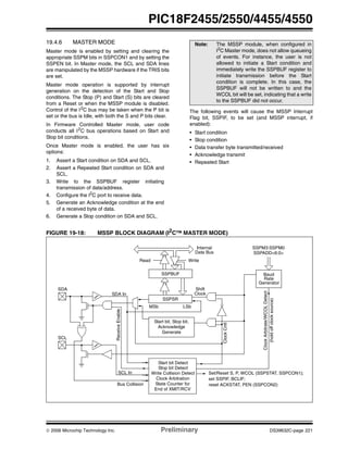
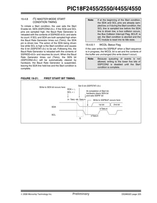
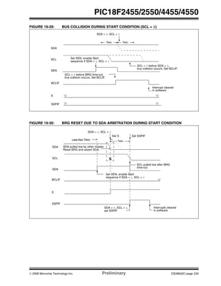
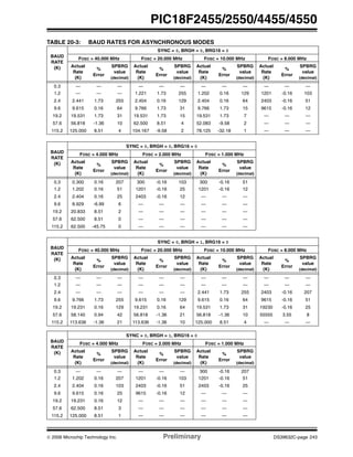
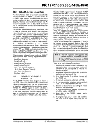
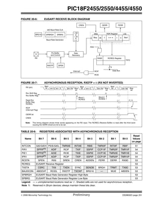
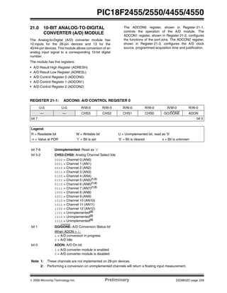
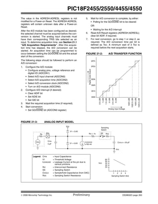
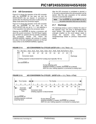
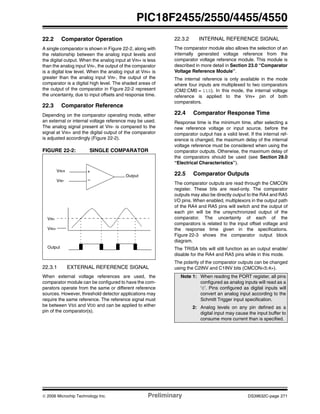
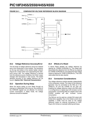
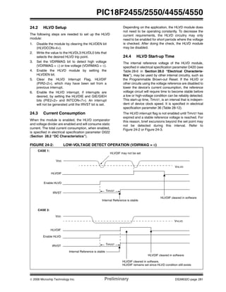
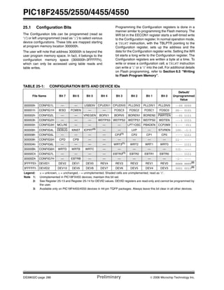
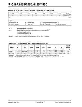
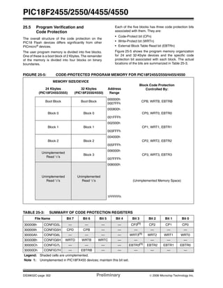
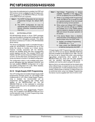
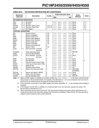
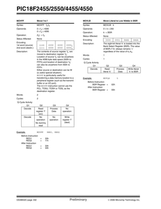
15.4 PWM Mode
In Pulse-Width Modulation (PWM) mode, the CCPx pin
produces up to a 10-bit resolution PWM output. Since
the CCP2 pin is multiplexed with a PORTB or PORTC
data latch, the appropriate TRIS bit must be cleared to
make the CCP2 pin an output.
Figure 15-3 shows a simplified block diagram of the
CCP module in PWM mode.
For a step-by-step procedure on how to set up the CCP
module for PWM operation, see Section 15.4.4
“Setup for PWM Operation”.
FIGURE 15-3: SIMPLIFIED PWM BLOCK
DIAGRAM
A PWM output (Figure 15-4) has a time base (period)
and a time that the output stays high (duty cycle). The
frequency of the PWM is the inverse of the period
(1/period).
FIGURE 15-4: PWM OUTPUT
15.4.1 PWM PERIOD
The PWM period is specified by writing to the PR2
register. The PWM period can be calculated using the
following formula:
EQUATION 15-1:
PWM frequency is defined as 1/[PWM period].
When TMR2 is equal to PR2, the following three events
occur on the next increment cycle:
• TMR2 is cleared
• The CCPx pin is set (exception: if PWM duty
cycle = 0%, the CCPx pin will not be set)
• The PWM duty cycle is latched from CCPRxL into
CCPRxH
15.4.2 PWM DUTY CYCLE
The PWM duty cycle is specified by writing to the
CCPRxL register and to the CCPxCON<5:4> bits. Up
to 10-bit resolution is available. The CCPRxL contains
the eight MSbs and the CCPxCON<5:4> bits contain
the two LSbs. This 10-bit value is represented by
CCPRxL:CCPxCON<5:4>. The following equation is
used to calculate the PWM duty cycle in time:
EQUATION 15-2:
CCPRxL and CCPxCON<5:4> can be written to at any
time, but the duty cycle value is not latched into
CCPRxH until after a match between PR2 and TMR2
occurs (i.e., the period is complete). In PWM mode,
CCPRxH is a read-only register.
Note: Clearing the CCP2CON register will force
the RB3 or RC1 output latch (depending
on device configuration) to the default low
level. This is not the PORTB or PORTC
I/O data latch.
CCPRxL
CCPRxH (Slave)
Comparator
TMR2
Comparator
PR2
(Note 1)
R Q
S
Duty Cycle Registers CCPxCON<5:4>
Clear Timer,
CCPx pin and
latch D.C.
Note 1: The 8-bit TMR2 value is concatenated with the 2-bit
internal Q clock, or 2 bits of the prescaler, to create the
10-bit time base.
CCPx
Corresponding
TRIS bit
Output
Period
Duty Cycle
TMR2 = PR2
TMR2 = Duty Cycle
TMR2 = PR2
Note: The Timer2 postscalers (see Section 13.0
“Timer2 Module”) are not used in the
determination of the PWM frequency. The
postscaler could be used to have a servo
update rate at a different frequency than
the PWM output.
PWM Period = [(PR2) + 1] • 4 • TOSC •
(TMR2 Prescale Value)
PWM Duty Cycle = (CCPRXL:CCPXCON<5:4>) •
TOSC • (TMR2 Prescale Value)](https://image.slidesharecdn.com/pic18f4550-140425123621-phpapp01/85/Pic18f4550-148-320.jpg)
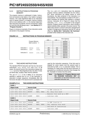
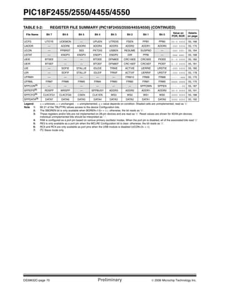
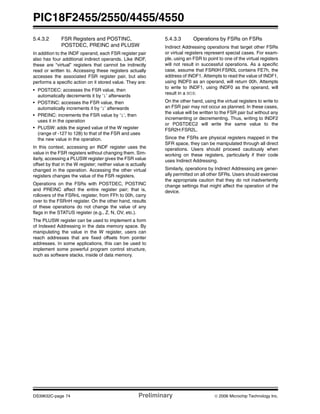
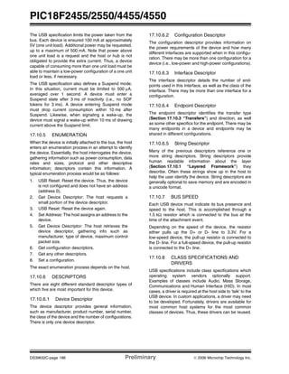
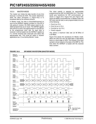
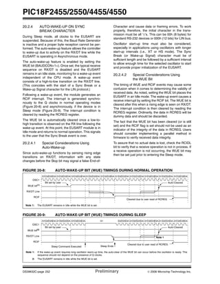
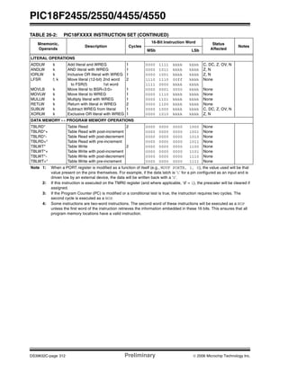
![© 2006 Microchip Technology Inc. Preliminary DS39632C-page 151
PIC18F2455/2550/4455/4550
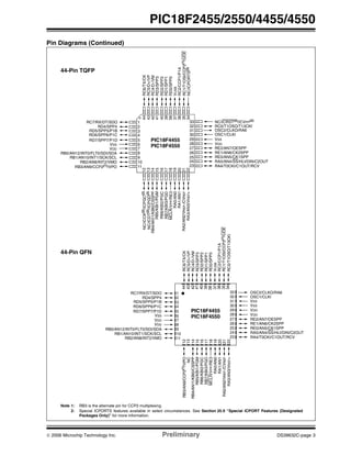
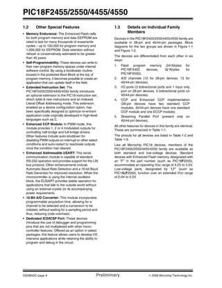
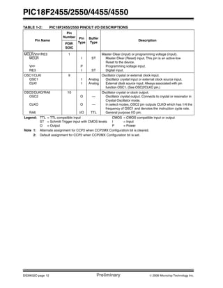
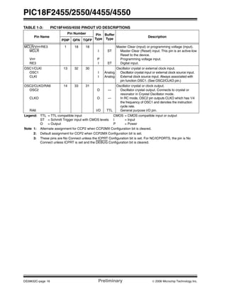
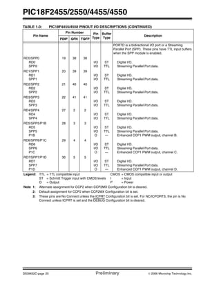
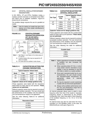
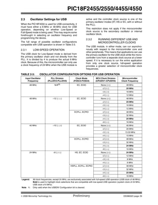
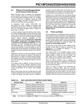
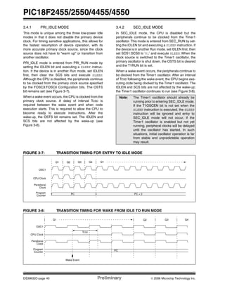
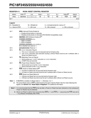
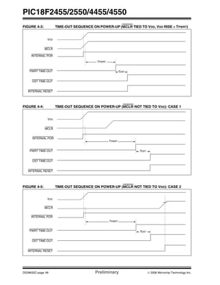
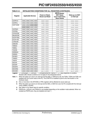
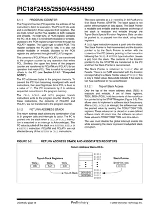
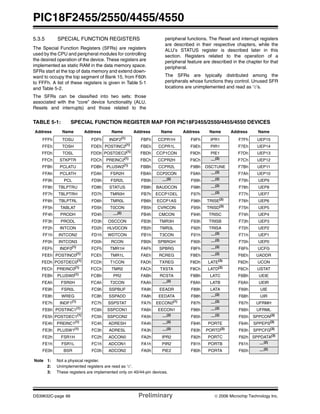
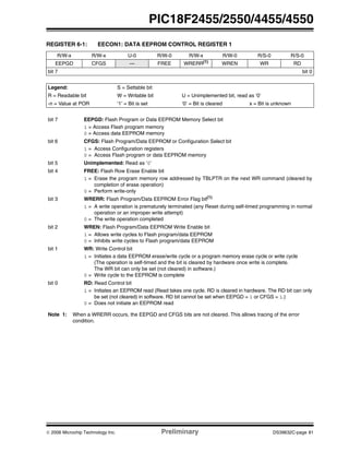
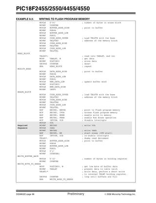
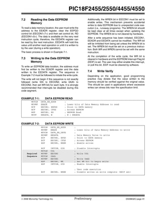
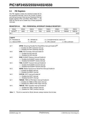
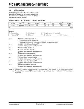
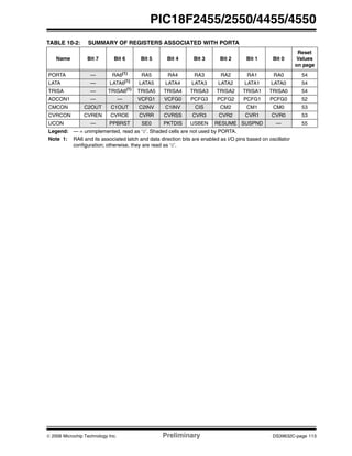
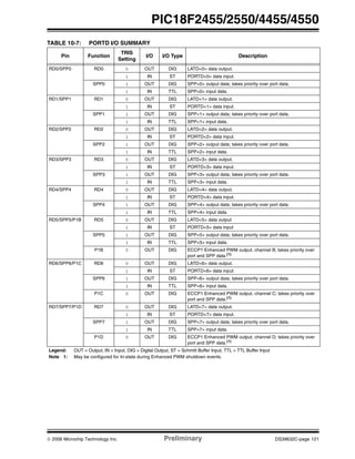
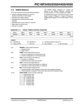
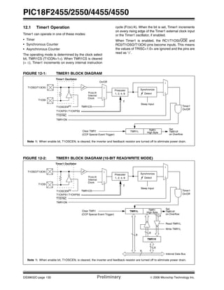
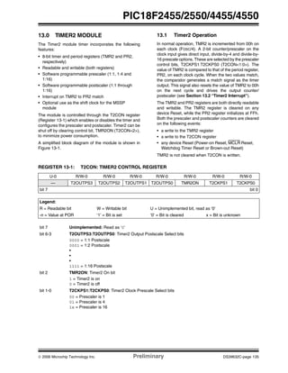
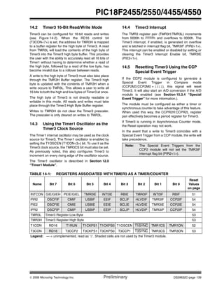
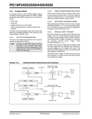
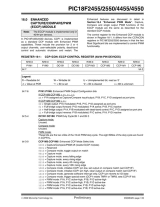
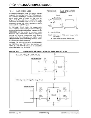
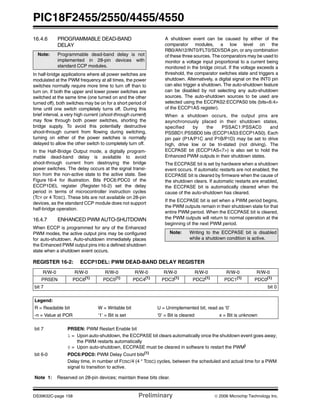
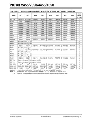
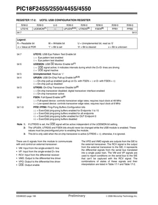
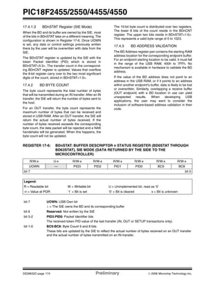
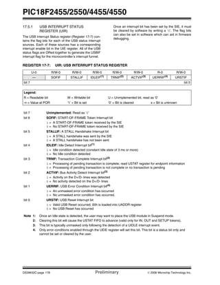
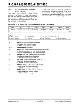
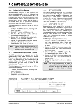
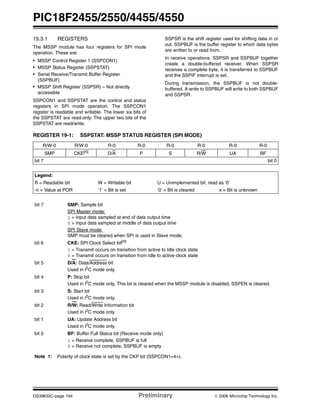
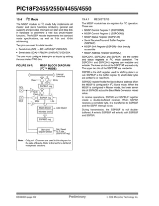
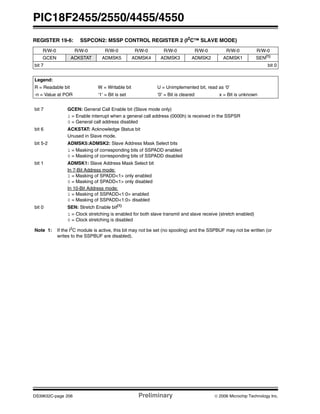
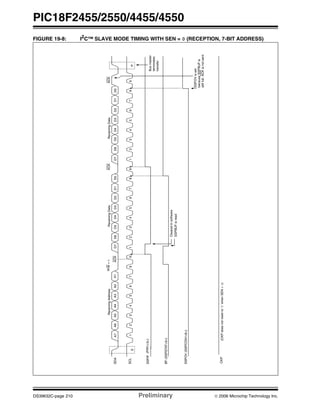
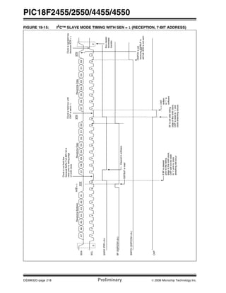
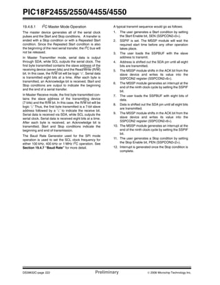
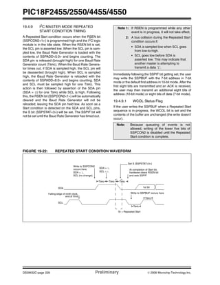
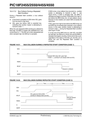
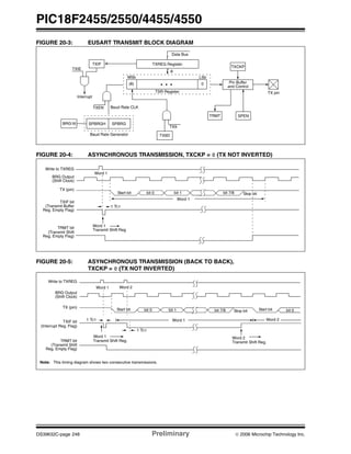
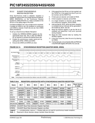
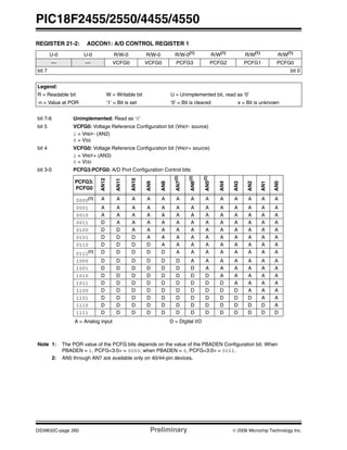
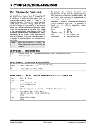
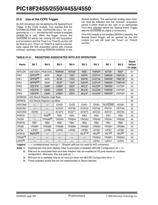
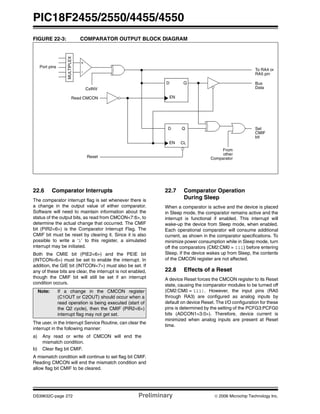
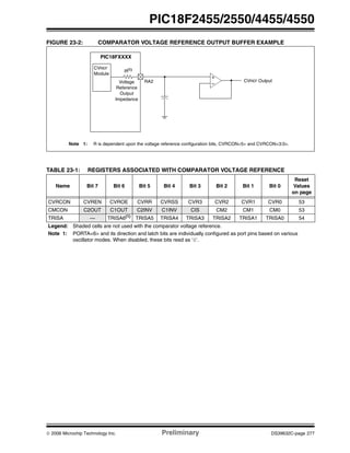
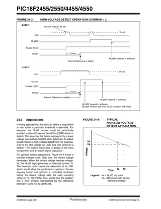
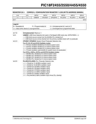
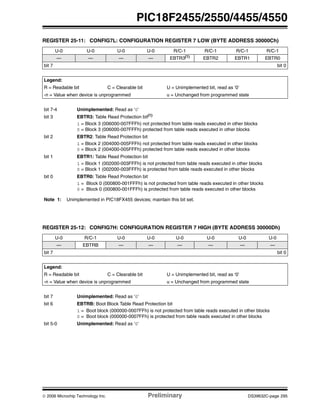
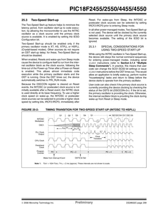
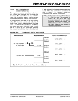
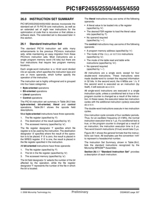
16.4 Enhanced PWM Mode
The Enhanced PWM mode provides additional PWM
output options for a broader range of control applica-
tions. The module is a backward compatible version of
the standard CCP module and offers up to four outputs,
designated P1A through P1D. Users are also able to
select the polarity of the signal (either active-high or
active-low). The module’s output mode and polarity are
configured by setting the P1M1:P1M0 and
CCP1M3:CCP1M0 bits of the CCP1CON register.
Figure 16-1 shows a simplified block diagram of PWM
operation. All control registers are double-buffered and
are loaded at the beginning of a new PWM cycle (the
period boundary when Timer2 resets) in order to
prevent glitches on any of the outputs. The exception is
the PWM Dead-Band Delay register, ECCP1DEL,
which is loaded at either the duty cycle boundary or the
boundary period (whichever comes first). Because of
the buffering, the module waits until the assigned timer
resets instead of starting immediately. This means that
Enhanced PWM waveforms do not exactly match the
standard PWM waveforms, but are instead offset by
one full instruction cycle (4 TOSC).
As before, the user must manually configure the
appropriate TRIS bits for output.
16.4.1 PWM PERIOD
The PWM period is specified by writing to the PR2
register. The PWM period can be calculated using the
following equation:
EQUATION 16-1:
PWM frequency is defined as 1/ [PWM period]. When
TMR2 is equal to PR2, the following three events occur
on the next increment cycle:
• TMR2 is cleared
• The CCP1 pin is set (if PWM duty cycle = 0%, the
CCP1 pin will not be set)
• The PWM duty cycle is copied from CCPR1L into
CCPR1H
FIGURE 16-1: SIMPLIFIED BLOCK DIAGRAM OF THE ENHANCED PWM MODULE
Note: The Timer2 postscaler (see Section 13.0
“Timer2 Module”) is not used in the
determination of the PWM frequency. The
postscaler could be used to have a servo
update rate at a different frequency than
the PWM output.
PWM Period = [(PR2) + 1] • 4 • TOSC •
(TMR2 Prescale Value)
CCPR1L
CCPR1H (Slave)
Comparator
TMR2
Comparator
PR2
(Note 1)
R Q
S
Duty Cycle Registers
CCP1CON<5:4>
Clear Timer,
set CCP1 pin and
latch D.C.
Note: The 8-bit TMR2 register is concatenated with the 2-bit internal Q clock, or 2 bits of the prescaler, to create the 10-bit time
base.
TRISD<4>
CCP1/P1A
TRISD<5>
P1B
TRISD<6>
TRISD<7>
P1D
Output
Controller
P1M1:P1M0
2
CCP1M3:CCP1M0
4
ECCP1DEL
CCP1/P1A
P1B
P1C
P1D
P1C](https://image.slidesharecdn.com/pic18f4550-140425123621-phpapp01/85/Pic18f4550-153-320.jpg)
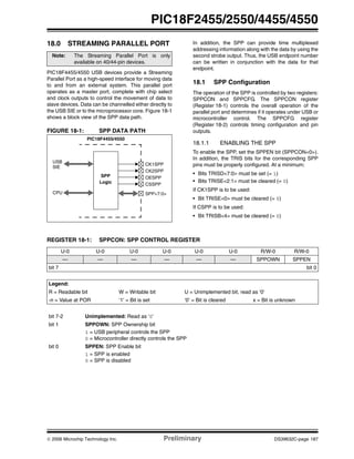
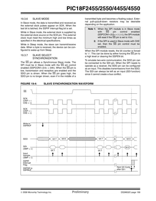
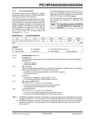
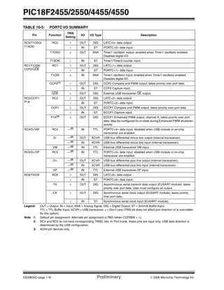
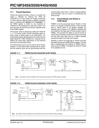
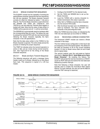
![© 2006 Microchip Technology Inc. Preliminary DS39632C-page 241
PIC18F2455/2550/4455/4550
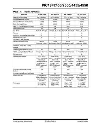
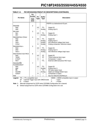
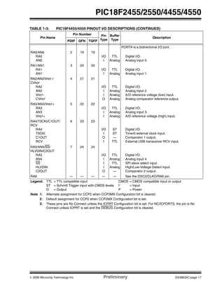
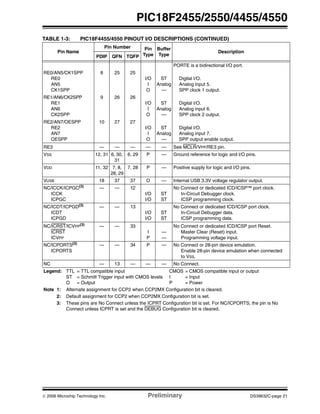
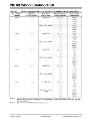
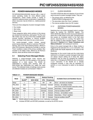
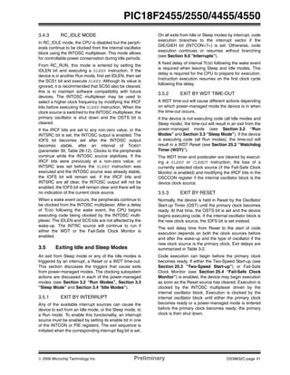
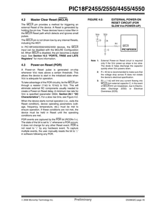
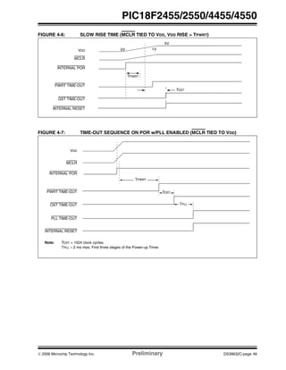
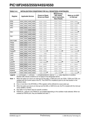
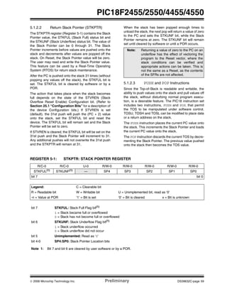
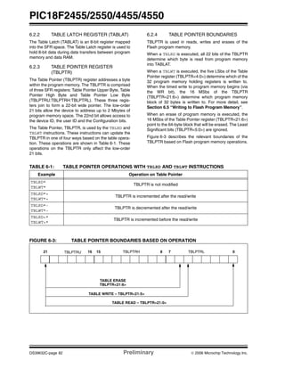
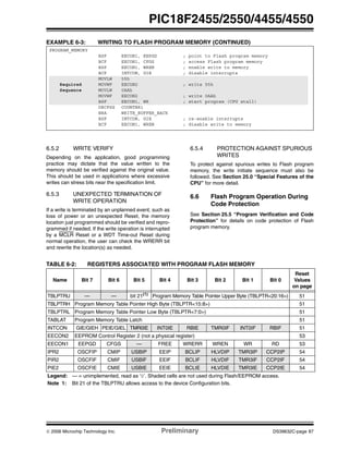
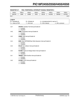
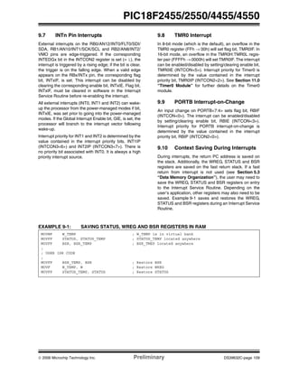
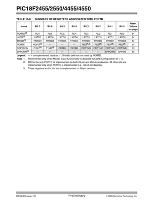
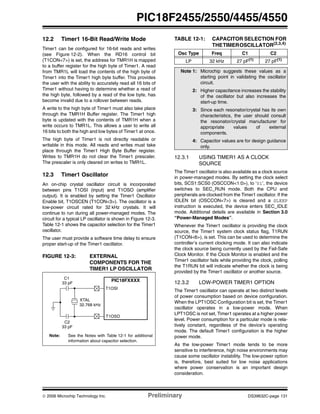
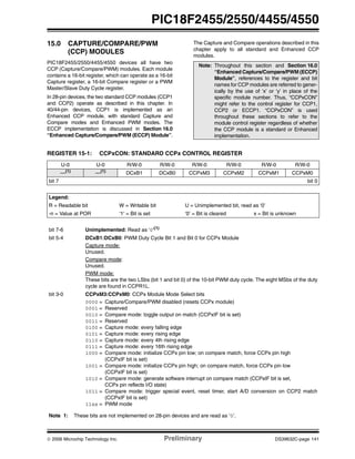
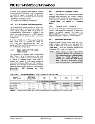
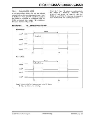
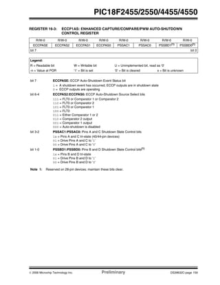
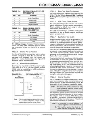
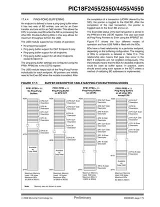
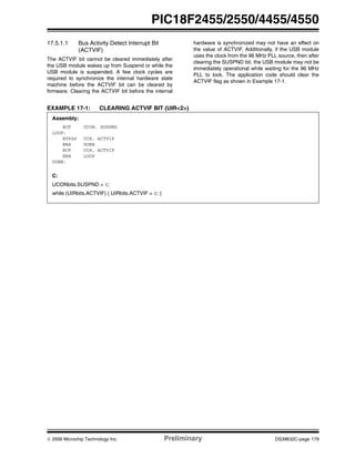
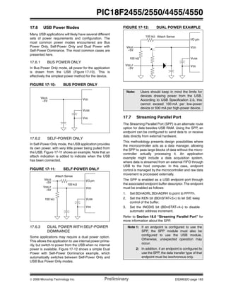
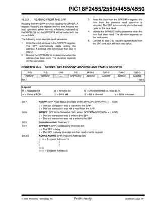
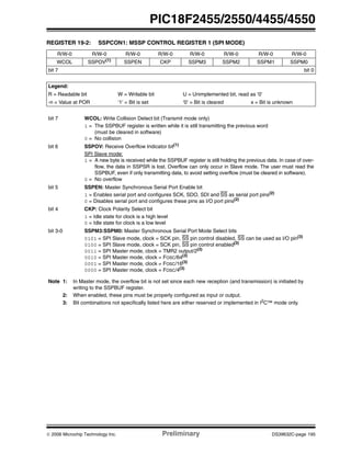
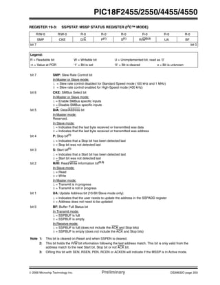
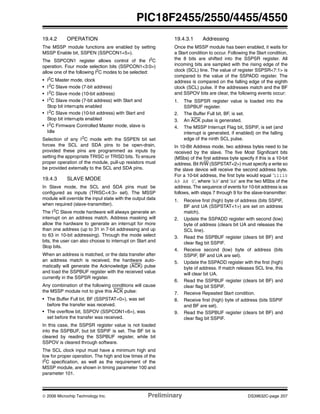
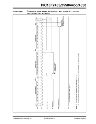
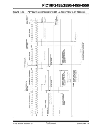
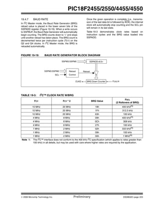
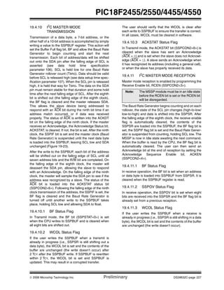
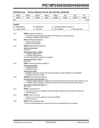
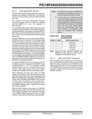
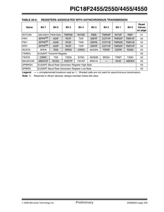
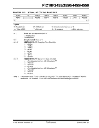
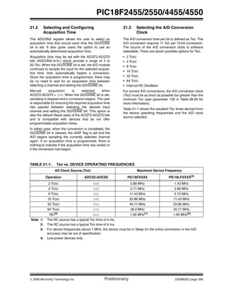
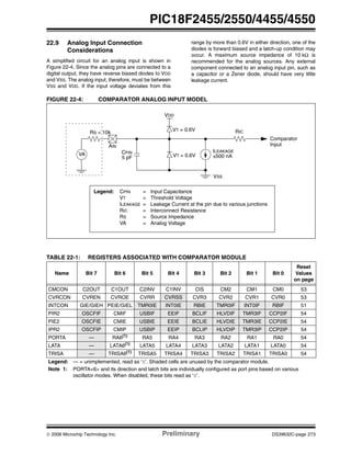
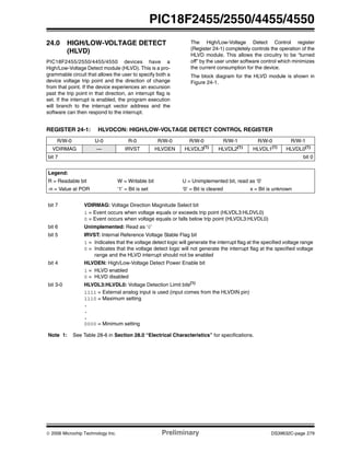
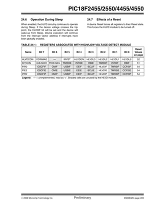
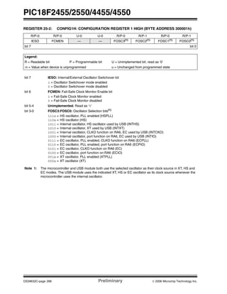
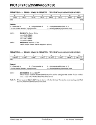
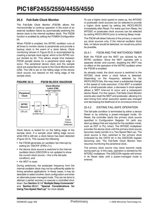
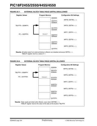
20.1 Baud Rate Generator (BRG)
The BRG is a dedicated 8-bit, or 16-bit, generator that
supports both the Asynchronous and Synchronous
modes of the EUSART. By default, the BRG operates
in 8-bit mode. Setting the BRG16 bit (BAUDCON<3>)
selects 16-bit mode.
The SPBRGH:SPBRG register pair controls the period
of a free-running timer. In Asynchronous mode, bits
BRGH (TXSTA<2>) and BRG16 (BAUDCON<3>) also
control the baud rate. In Synchronous mode, BRGH is
ignored. Table 20-1 shows the formula for computation
of the baud rate for different EUSART modes which
only apply in Master mode (internally generated clock).
Given the desired baud rate and FOSC, the nearest
integer value for the SPBRGH:SPBRG registers can be
calculated using the formulas in Table 20-1. From this,
the error in baud rate can be determined. An example
calculation is shown in Example 20-1. Typical baud
rates and error values for the various Asynchronous
modes are shown in Table 20-2. It may be advantageous
to use the high baud rate (BRGH = 1), or the 16-bit BRG
to reduce the baud rate error, or achieve a slow baud
rate for a fast oscillator frequency.
Writing a new value to the SPBRGH:SPBRG registers
causes the BRG timer to be reset (or cleared). This
ensures the BRG does not wait for a timer overflow
before outputting the new baud rate.
20.1.1 OPERATION IN POWER-MANAGED
MODES
The device clock is used to generate the desired baud
rate. When one of the power-managed modes is
entered, the new clock source may be operating at a
different frequency. This may require an adjustment to
the value in the SPBRG register pair.
20.1.2 SAMPLING
The data on the RX pin is sampled three times by a
majority detect circuit to determine if a high or a low
level is present at the RX pin.
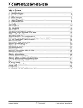
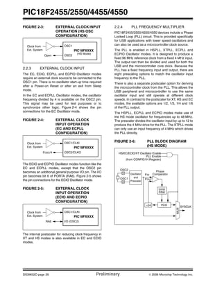
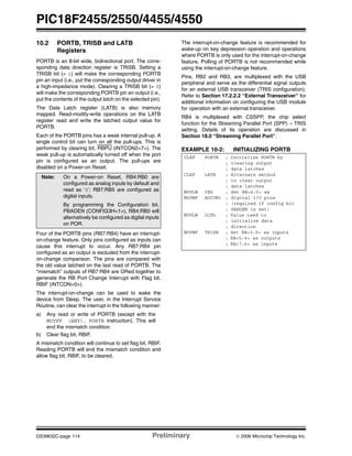
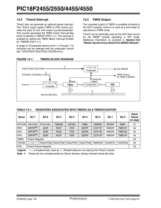
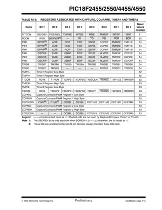
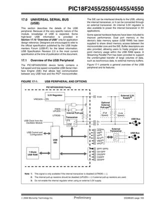
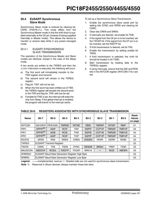
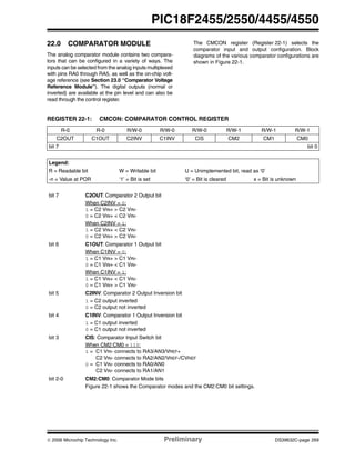
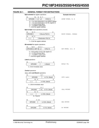
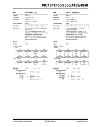
TABLE 20-1: BAUD RATE FORMULAS
Configuration Bits
BRG/EUSART Mode Baud Rate Formula
SYNC BRG16 BRGH
0 0 0 8-bit/Asynchronous FOSC/[64 (n + 1)]
0 0 1 8-bit/Asynchronous
FOSC/[16 (n + 1)]
0 1 0 16-bit/Asynchronous
0 1 1 16-bit/Asynchronous
FOSC/[4 (n + 1)]1 0 x 8-bit/Synchronous
1 1 x 16-bit/Synchronous
Legend: x = Don’t care, n = value of SPBRGH:SPBRG register pair](https://image.slidesharecdn.com/pic18f4550-140425123621-phpapp01/85/Pic18f4550-243-320.jpg)
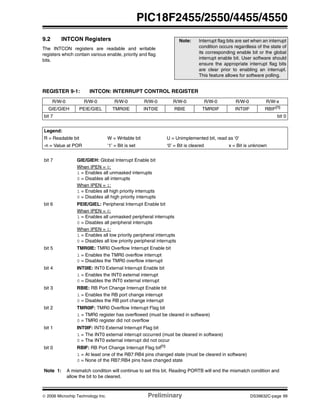
![PIC18F2455/2550/4455/4550
DS39632C-page 242 Preliminary © 2006 Microchip Technology Inc.
EXAMPLE 20-1: CALCULATING BAUD RATE ERROR
TABLE 20-2: REGISTERS ASSOCIATED WITH BAUD RATE GENERATOR
For a device with FOSC of 16 MHz, desired baud rate of 9600, Asynchronous mode, 8-bit BRG:
Desired Baud Rate = FOSC/(64 ([SPBRGH:SPBRG] + 1))
Solving for SPBRGH:SPBRG:
X = ((FOSC/Desired Baud Rate)/64) – 1
= ((16000000/9600)/64) – 1
= [25.042] = 25
Calculated Baud Rate = 16000000/(64 (25 + 1))
= 9615
Error = (Calculated Baud Rate – Desired Baud Rate)/Desired Baud Rate
= (9615 – 9600)/9600 = 0.16%
Name Bit 7 Bit 6 Bit 5 Bit 4 Bit 3 Bit 2 Bit 1 Bit 0
Reset Values
on page
TXSTA CSRC TX9 TXEN SYNC SENDB BRGH TRMT TX9D 53
RCSTA SPEN RX9 SREN CREN ADDEN FERR OERR RX9D 53
BAUDCON ABDOVF RCIDL RXDTP TXCKP BRG16 — WUE ABDEN 53
SPBRGH EUSART Baud Rate Generator Register High Byte 53
SPBRG EUSART Baud Rate Generator Register Low Byte 53
Legend: — = unimplemented, read as ‘0’. Shaded cells are not used by the BRG.](https://image.slidesharecdn.com/pic18f4550-140425123621-phpapp01/85/Pic18f4550-244-320.jpg)


![PIC18F2455/2550/4455/4550
DS39632C-page 308 Preliminary © 2006 Microchip Technology Inc.
TABLE 26-1: OPCODE FIELD DESCRIPTIONS
Field Description
a RAM access bit
a = 0: RAM location in Access RAM (BSR register is ignored)
a = 1: RAM bank is specified by BSR register
bbb Bit address within an 8-bit file register (0 to 7).
BSR Bank Select Register. Used to select the current RAM bank.
C, DC, Z, OV, N ALU Status bits: Carry, Digit Carry, Zero, Overflow, Negative.
d Destination select bit
d = 0: store result in WREG
d = 1: store result in file register f
dest Destination: either the WREG register or the specified register file location.
f 8-bit register file address (00h to FFh) or 2-bit FSR designator (0h to 3h).
fs 12-bit register file address (000h to FFFh). This is the source address.
fd 12-bit register file address (000h to FFFh). This is the destination address.
GIE Global Interrupt Enable bit.
k Literal field, constant data or label (may be either an 8-bit, 12-bit or a 20-bit value).
label Label name.
mm The mode of the TBLPTR register for the table read and table write instructions.
Only used with table read and table write instructions:
* No change to register (such as TBLPTR with table reads and writes)
*+ Post-Increment register (such as TBLPTR with table reads and writes)
*- Post-Decrement register (such as TBLPTR with table reads and writes)
+* Pre-Increment register (such as TBLPTR with table reads and writes)
n The relative address (2’s complement number) for relative branch instructions or the direct address for
Call/Branch and Return instructions.
PC Program Counter.
PCL Program Counter Low Byte.
PCH Program Counter High Byte.
PCLATH Program Counter High Byte Latch.
PCLATU Program Counter Upper Byte Latch.
PD Power-Down bit.
PRODH Product of Multiply High Byte.
PRODL Product of Multiply Low Byte.
s Fast Call/Return mode select bit
s = 0: do not update into/from shadow registers
s = 1: certain registers loaded into/from shadow registers (Fast mode)
TBLPTR 21-bit Table Pointer (points to a program memory location).
TABLAT 8-bit Table Latch.
TO Time-out bit.
TOS Top-of-Stack.
u Unused or unchanged.
WDT Watchdog Timer.
WREG Working register (accumulator).
x Don’t care (‘0’ or ‘1’). The assembler will generate code with x = 0. It is the recommended form of use for
compatibility with all Microchip software tools.
zs 7-bit offset value for indirect addressing of register files (source).
zd 7-bit offset value for indirect addressing of register files (destination).
{ } Optional argument.
[text] Indicates an indexed address.
(text) The contents of text.
[expr]<n> Specifies bit n of the register indicated by the pointer expr.
→ Assigned to.
< > Register bit field.
∈ In the set of.
italics User-defined term (font is Courier).](https://image.slidesharecdn.com/pic18f4550-140425123621-phpapp01/85/Pic18f4550-310-320.jpg)
![© 2006 Microchip Technology Inc. Preliminary DS39632C-page 313
PIC18F2455/2550/4455/4550
26.1.1 STANDARD INSTRUCTION SET
ADDLW ADD Literal to W
Syntax: ADDLW k
Operands: 0 ≤ k ≤ 255
Operation: (W) + k → W
Status Affected: N, OV, C, DC, Z
Encoding: 0000 1111 kkkk kkkk
Description: The contents of W are added to the
8-bit literal ‘k’ and the result is placed in
W.
Words: 1
Cycles: 1
Q Cycle Activity:
Q1 Q2 Q3 Q4
Decode Read
literal ‘k’
Process
Data
Write to W
Example: ADDLW 15h
Before Instruction
W = 10h
After Instruction
W = 25h
ADDWF ADD W to f
Syntax: ADDWF f {,d {,a}}
Operands: 0 ≤ f ≤ 255
d ∈ [0,1]
a ∈ [0,1]
Operation: (W) + (f) → dest
Status Affected: N, OV, C, DC, Z
Encoding: 0010 01da ffff ffff
Description: Add W to register ‘f’. If ‘d’ is ‘0’, the
result is stored in W. If ‘d’ is ‘1’, the
result is stored back in register ‘f’
(default).
If ‘a’ is ‘0’, the Access Bank is selected.
If ‘a’ is ‘1’, the BSR is used to select the
GPR bank (default).
If ‘a’ is ‘0’ and the extended instruction
set is enabled, this instruction operates
in Indexed Literal Offset Addressing
mode whenever f ≤ 95 (5Fh). See
Section 26.2.3 “Byte-Oriented and
Bit-Oriented Instructions in Indexed
Literal Offset Mode” for details.
Words: 1
Cycles: 1
Q Cycle Activity:
Q1 Q2 Q3 Q4
Decode Read
register ‘f’
Process
Data
Write to
destination
Example: ADDWF REG, 0, 0
Before Instruction
W = 17h
REG = 0C2h
After Instruction
W = 0D9h
REG = 0C2h
Note: All PIC18 instructions may take an optional label argument, preceding the instruction mnemonic, for use in
symbolic addressing. If a label is used, the instruction format then becomes: {label} instruction argument(s).](https://image.slidesharecdn.com/pic18f4550-140425123621-phpapp01/85/Pic18f4550-315-320.jpg)
![PIC18F2455/2550/4455/4550
DS39632C-page 314 Preliminary © 2006 Microchip Technology Inc.
ADDWFC ADD W and Carry bit to f
Syntax: ADDWFC f {,d {,a}}
Operands: 0 ≤ f ≤ 255
d ∈ [0,1]
a ∈ [0,1]
Operation: (W) + (f) + (C) → dest
Status Affected: N, OV, C, DC, Z
Encoding: 0010 00da ffff ffff
Description: Add W, the Carry flag and data memory
location ‘f’. If ‘d’ is ‘0’, the result is
placed in W. If ‘d’ is ‘1’, the result is
placed in data memory location ‘f’.
If ‘a’ is ‘0’, the Access Bank is selected.
If ‘a’ is ‘1’, the BSR is used to select the
GPR bank (default).
If ‘a’ is ‘0’ and the extended instruction
set is enabled, this instruction operates
in Indexed Literal Offset Addressing
mode whenever f ≤ 95 (5Fh). See
Section 26.2.3 “Byte-Oriented and
Bit-Oriented Instructions in Indexed
Literal Offset Mode” for details.
Words: 1
Cycles: 1
Q Cycle Activity:
Q1 Q2 Q3 Q4
Decode Read
register ‘f’
Process
Data
Write to
destination
Example: ADDWFC REG, 0, 1
Before Instruction
Carry bit = 1
REG = 02h
W = 4Dh
After Instruction
Carry bit = 0
REG = 02h
W = 50h
ANDLW AND Literal with W
Syntax: ANDLW k
Operands: 0 ≤ k ≤ 255
Operation: (W) .AND. k → W
Status Affected: N, Z
Encoding: 0000 1011 kkkk kkkk
Description: The contents of W are ANDed with the
8-bit literal ‘k’. The result is placed in W.
Words: 1
Cycles: 1
Q Cycle Activity:
Q1 Q2 Q3 Q4
Decode Read literal
‘k’
Process
Data
Write to W
Example: ANDLW 05Fh
Before Instruction
W = A3h
After Instruction
W = 03h](https://image.slidesharecdn.com/pic18f4550-140425123621-phpapp01/85/Pic18f4550-316-320.jpg)
![© 2006 Microchip Technology Inc. Preliminary DS39632C-page 315
PIC18F2455/2550/4455/4550
ANDWF AND W with f
Syntax: ANDWF f {,d {,a}}
Operands: 0 ≤ f ≤ 255
d ∈ [0,1]
a ∈ [0,1]
Operation: (W) .AND. (f) → dest
Status Affected: N, Z
Encoding: 0001 01da ffff ffff
Description: The contents of W are ANDed with
register ‘f’. If ‘d’ is ‘0’, the result is stored
in W. If ‘d’ is ‘1’, the result is stored back
in register ‘f’ (default).
If ‘a’ is ‘0’, the Access Bank is selected.
If ‘a’ is ‘1’, the BSR is used to select the
GPR bank (default).
If ‘a’ is ‘0’ and the extended instruction
set is enabled, this instruction operates
in Indexed Literal Offset Addressing
mode whenever f ≤ 95 (5Fh). See
Section 26.2.3 “Byte-Oriented and
Bit-Oriented Instructions in Indexed
Literal Offset Mode” for details.
Words: 1
Cycles: 1
Q Cycle Activity:
Q1 Q2 Q3 Q4
Decode Read
register ‘f’
Process
Data
Write to
destination
Example: ANDWF REG, 0, 0
Before Instruction
W = 17h
REG = C2h
After Instruction
W = 02h
REG = C2h
BC Branch if Carry
Syntax: BC n
Operands: -128 ≤ n ≤ 127
Operation: if Carry bit is ‘1’
(PC) + 2 + 2n → PC
Status Affected: None
Encoding: 1110 0010 nnnn nnnn
Description: If the Carry bit is ‘1’, then the program
will branch.
The 2’s complement number ‘2n’ is
added to the PC. Since the PC will have
incremented to fetch the next
instruction, the new address will be
PC + 2 + 2n. This instruction is then a
two-cycle instruction.
Words: 1
Cycles: 1(2)
Q Cycle Activity:
If Jump:
Q1 Q2 Q3 Q4
Decode Read literal
‘n’
Process
Data
Write to PC
No
operation
No
operation
No
operation
No
operation
If No Jump:
Q1 Q2 Q3 Q4
Decode Read literal
‘n’
Process
Data
No
operation
Example: HERE BC 5
Before Instruction
PC = address (HERE)
After Instruction
If Carry = 1;
PC = address (HERE + 12)
If Carry = 0;
PC = address (HERE + 2)](https://image.slidesharecdn.com/pic18f4550-140425123621-phpapp01/85/Pic18f4550-317-320.jpg)
![PIC18F2455/2550/4455/4550
DS39632C-page 316 Preliminary © 2006 Microchip Technology Inc.
BCF Bit Clear f
Syntax: BCF f, b {,a}
Operands: 0 ≤ f ≤ 255
0 ≤ b ≤ 7
a ∈ [0,1]
Operation: 0 → f<b>
Status Affected: None
Encoding: 1001 bbba ffff ffff
Description: Bit ‘b’ in register ‘f’ is cleared.
If ‘a’ is ‘0’, the Access Bank is selected.
If ‘a’ is ‘1’, the BSR is used to select the
GPR bank (default).
If ‘a’ is ‘0’ and the extended instruction
set is enabled, this instruction operates
in Indexed Literal Offset Addressing
mode whenever f ≤ 95 (5Fh). See
Section 26.2.3 “Byte-Oriented and
Bit-Oriented Instructions in Indexed
Literal Offset Mode” for details.
Words: 1
Cycles: 1
Q Cycle Activity:
Q1 Q2 Q3 Q4
Decode Read
register ‘f’
Process
Data
Write
register ‘f’
Example: BCF FLAG_REG, 7, 0
Before Instruction
FLAG_REG = C7h
After Instruction
FLAG_REG = 47h
BN Branch if Negative
Syntax: BN n
Operands: -128 ≤ n ≤ 127
Operation: if Negative bit is ‘1’
(PC) + 2 + 2n → PC
Status Affected: None
Encoding: 1110 0110 nnnn nnnn
Description: If the Negative bit is ‘1’, then the
program will branch.
The 2’s complement number ‘2n’ is
added to the PC. Since the PC will have
incremented to fetch the next
instruction, the new address will be
PC + 2 + 2n. This instruction is then a
two-cycle instruction.
Words: 1
Cycles: 1(2)
Q Cycle Activity:
If Jump:
Q1 Q2 Q3 Q4
Decode Read literal
‘n’
Process
Data
Write to PC
No
operation
No
operation
No
operation
No
operation
If No Jump:
Q1 Q2 Q3 Q4
Decode Read literal
‘n’
Process
Data
No
operation
Example: HERE BN Jump
Before Instruction
PC = address (HERE)
After Instruction
If Negative = 1;
PC = address (Jump)
If Negative = 0;
PC = address (HERE + 2)](https://image.slidesharecdn.com/pic18f4550-140425123621-phpapp01/85/Pic18f4550-318-320.jpg)
![© 2006 Microchip Technology Inc. Preliminary DS39632C-page 319
PIC18F2455/2550/4455/4550
BRA Unconditional Branch
Syntax: BRA n
Operands: -1024 ≤ n ≤ 1023
Operation: (PC) + 2 + 2n → PC
Status Affected: None
Encoding: 1101 0nnn nnnn nnnn
Description: Add the 2’s complement number ‘2n’ to
the PC. Since the PC will have
incremented to fetch the next
instruction, the new address will be
PC + 2 + 2n. This instruction is a
two-cycle instruction.
Words: 1
Cycles: 2
Q Cycle Activity:
Q1 Q2 Q3 Q4
Decode Read literal
‘n’
Process
Data
Write to PC
No
operation
No
operation
No
operation
No
operation
Example: HERE BRA Jump
Before Instruction
PC = address (HERE)
After Instruction
PC = address (Jump)
BSF Bit Set f
Syntax: BSF f, b {,a}
Operands: 0 ≤ f ≤ 255
0 ≤ b ≤ 7
a ∈ [0,1]
Operation: 1 → f<b>
Status Affected: None
Encoding: 1000 bbba ffff ffff
Description: Bit ‘b’ in register ‘f’ is set.
If ‘a’ is ‘0’, the Access Bank is selected.
If ‘a’ is ‘1’, the BSR is used to select the
GPR bank (default).
If ‘a’ is ‘0’ and the extended instruction
set is enabled, this instruction operates
in Indexed Literal Offset Addressing
mode whenever f ≤ 95 (5Fh). See
Section 26.2.3 “Byte-Oriented and
Bit-Oriented Instructions in Indexed
Literal Offset Mode” for details.
Words: 1
Cycles: 1
Q Cycle Activity:
Q1 Q2 Q3 Q4
Decode Read
register ‘f’
Process
Data
Write
register ‘f’
Example: BSF FLAG_REG, 7, 1
Before Instruction
FLAG_REG = 0Ah
After Instruction
FLAG_REG = 8Ah](https://image.slidesharecdn.com/pic18f4550-140425123621-phpapp01/85/Pic18f4550-321-320.jpg)
![PIC18F2455/2550/4455/4550
DS39632C-page 320 Preliminary © 2006 Microchip Technology Inc.
BTFSC Bit Test File, Skip if Clear
Syntax: BTFSC f, b {,a}
Operands: 0 ≤ f ≤ 255
0 ≤ b ≤ 7
a ∈ [0,1]
Operation: skip if (f<b>) = 0
Status Affected: None
Encoding: 1011 bbba ffff ffff
Description: If bit ‘b’ in register ‘f’ is ‘0’, then the next
instruction is skipped. If bit ‘b’ is ‘0’, then
the next instruction fetched during the
current instruction execution is discarded
and a NOP is executed instead, making
this a two-cycle instruction.
If ‘a’ is ‘0’, the Access Bank is selected. If
‘a’ is ‘1’, the BSR is used to select the
GPR bank (default).
If ‘a’ is ‘0’ and the extended instruction
set is enabled, this instruction operates in
Indexed Literal Offset Addressing
mode whenever f ≤ 95 (5Fh).
See Section 26.2.3 “Byte-Oriented and
Bit-Oriented Instructions in Indexed
Literal Offset Mode” for details.
Words: 1
Cycles: 1(2)
Note: 3 cycles if skip and followed
by a 2-word instruction.
Q Cycle Activity:
Q1 Q2 Q3 Q4
Decode Read
register ‘f’
Process
Data
No
operation
If skip:
Q1 Q2 Q3 Q4
No
operation
No
operation
No
operation
No
operation
If skip and followed by 2-word instruction:
Q1 Q2 Q3 Q4
No
operation
No
operation
No
operation
No
operation
No
operation
No
operation
No
operation
No
operation
Example: HERE
FALSE
TRUE
BTFSC
:
:
FLAG, 1, 0
Before Instruction
PC = address (HERE)
After Instruction
If FLAG<1> = 0;
PC = address (TRUE)
If FLAG<1> = 1;
PC = address (FALSE)
BTFSS Bit Test File, Skip if Set
Syntax: BTFSS f, b {,a}
Operands: 0 ≤ f ≤ 255
0 ≤ b < 7
a ∈ [0,1]
Operation: skip if (f<b>) = 1
Status Affected: None
Encoding: 1010 bbba ffff ffff
Description: If bit ‘b’ in register ‘f’ is ‘1’, then the next
instruction is skipped. If bit ‘b’ is ‘1’, then
the next instruction fetched during the
current instruction execution is discarded
and a NOP is executed instead, making
this a two-cycle instruction.
If ‘a’ is ‘0’, the Access Bank is selected. If
‘a’ is ‘1’, the BSR is used to select the
GPR bank (default).
If ‘a’ is ‘0’ and the extended instruction
set is enabled, this instruction operates
in Indexed Literal Offset Addressing
mode whenever f ≤ 95 (5Fh).
See Section 26.2.3 “Byte-Oriented and
Bit-Oriented Instructions in Indexed
Literal Offset Mode” for details.
Words: 1
Cycles: 1(2)
Note: 3 cycles if skip and followed
by a 2-word instruction.
Q Cycle Activity:
Q1 Q2 Q3 Q4
Decode Read
register ‘f’
Process
Data
No
operation
If skip:
Q1 Q2 Q3 Q4
No
operation
No
operation
No
operation
No
operation
If skip and followed by 2-word instruction:
Q1 Q2 Q3 Q4
No
operation
No
operation
No
operation
No
operation
No
operation
No
operation
No
operation
No
operation
Example: HERE
FALSE
TRUE
BTFSS
:
:
FLAG, 1, 0
Before Instruction
PC = address (HERE)
After Instruction
If FLAG<1> = 0;
PC = address (FALSE)
If FLAG<1> = 1;
PC = address (TRUE)](https://image.slidesharecdn.com/pic18f4550-140425123621-phpapp01/85/Pic18f4550-322-320.jpg)
![© 2006 Microchip Technology Inc. Preliminary DS39632C-page 321
PIC18F2455/2550/4455/4550
BTG Bit Toggle f
Syntax: BTG f, b {,a}
Operands: 0 ≤ f ≤ 255
0 ≤ b < 7
a ∈ [0,1]
Operation: (f<b>) → f<b>
Status Affected: None
Encoding: 0111 bbba ffff ffff
Description: Bit ‘b’ in data memory location ‘f’ is
inverted.
If ‘a’ is ‘0’, the Access Bank is selected.
If ‘a’ is ‘1’, the BSR is used to select the
GPR bank (default).
If ‘a’ is ‘0’ and the extended instruction
set is enabled, this instruction operates
in Indexed Literal Offset Addressing
mode whenever f ≤ 95 (5Fh). See
Section 26.2.3 “Byte-Oriented and
Bit-Oriented Instructions in Indexed
Literal Offset Mode” for details.
Words: 1
Cycles: 1
Q Cycle Activity:
Q1 Q2 Q3 Q4
Decode Read
register ‘f’
Process
Data
Write
register ‘f’
Example: BTG PORTC, 4, 0
Before Instruction:
PORTC = 0111 0101 [75h]
After Instruction:
PORTC = 0110 0101 [65h]
BOV Branch if Overflow
Syntax: BOV n
Operands: -128 ≤ n ≤ 127
Operation: if Overflow bit is ‘1’
(PC) + 2 + 2n → PC
Status Affected: None
Encoding: 1110 0100 nnnn nnnn
Description: If the Overflow bit is ‘1’, then the
program will branch.
The 2’s complement number ‘2n’ is
added to the PC. Since the PC will have
incremented to fetch the next
instruction, the new address will be
PC + 2 + 2n. This instruction is then a
two-cycle instruction.
Words: 1
Cycles: 1(2)
Q Cycle Activity:
If Jump:
Q1 Q2 Q3 Q4
Decode Read literal
‘n’
Process
Data
Write to PC
No
operation
No
operation
No
operation
No
operation
If No Jump:
Q1 Q2 Q3 Q4
Decode Read literal
‘n’
Process
Data
No
operation
Example: HERE BOV Jump
Before Instruction
PC = address (HERE)
After Instruction
If Overflow = 1;
PC = address (Jump)
If Overflow = 0;
PC = address (HERE + 2)](https://image.slidesharecdn.com/pic18f4550-140425123621-phpapp01/85/Pic18f4550-323-320.jpg)
![PIC18F2455/2550/4455/4550
DS39632C-page 322 Preliminary © 2006 Microchip Technology Inc.
BZ Branch if Zero
Syntax: BZ n
Operands: -128 ≤ n ≤ 127
Operation: if Zero bit is ‘1’
(PC) + 2 + 2n → PC
Status Affected: None
Encoding: 1110 0000 nnnn nnnn
Description: If the Zero bit is ‘1’, then the program
will branch.
The 2’s complement number ‘2n’ is
added to the PC. Since the PC will have
incremented to fetch the next
instruction, the new address will be
PC + 2 + 2n. This instruction is then a
two-cycle instruction.
Words: 1
Cycles: 1(2)
Q Cycle Activity:
If Jump:
Q1 Q2 Q3 Q4
Decode Read literal
‘n’
Process
Data
Write to PC
No
operation
No
operation
No
operation
No
operation
If No Jump:
Q1 Q2 Q3 Q4
Decode Read literal
‘n’
Process
Data
No
operation
Example: HERE BZ Jump
Before Instruction
PC = address (HERE)
After Instruction
If Zero = 1;
PC = address (Jump)
If Zero = 0;
PC = address (HERE + 2)
CALL Subroutine Call
Syntax: CALL k {,s}
Operands: 0 ≤ k ≤ 1048575
s ∈ [0,1]
Operation: (PC) + 4 → TOS,
k → PC<20:1>,
if s = 1
(W) → WS,
(STATUS) → STATUSS,
(BSR) → BSRS
Status Affected: None
Encoding:
1st word (k<7:0>)
2nd word(k<19:8>)
1110
1111
110s
k19kkk
k7kkk
kkkk
kkkk0
kkkk8
Description: Subroutine call of entire 2-Mbyte
memory range. First, return address
(PC + 4) is pushed onto the return
stack. If ‘s’ = 1, the W, STATUS and
BSR
registers are also pushed into their
respective shadow registers, WS,
STATUSS and BSRS. If ‘s’ = 0, no
update occurs (default). Then, the
20-bit value ‘k’ is loaded into PC<20:1>.
CALL is a two-cycle instruction.
Words: 2
Cycles: 2
Q Cycle Activity:
Q1 Q2 Q3 Q4
Decode Read literal
‘k’<7:0>,
Push PC to
stack
Read literal
‘k’<19:8>,
Write to PC
No
operation
No
operation
No
operation
No
operation
Example: HERE CALL THERE,1
Before Instruction
PC = address (HERE)
After Instruction
PC = address (THERE)
TOS = address (HERE + 4)
WS = W
BSRS = BSR
STATUSS = STATUS](https://image.slidesharecdn.com/pic18f4550-140425123621-phpapp01/85/Pic18f4550-324-320.jpg)
![© 2006 Microchip Technology Inc. Preliminary DS39632C-page 323
PIC18F2455/2550/4455/4550
CLRF Clear f
Syntax: CLRF f {,a}
Operands: 0 ≤ f ≤ 255
a ∈ [0,1]
Operation: 000h → f,
1 → Z
Status Affected: Z
Encoding: 0110 101a ffff ffff
Description: Clears the contents of the specified
register.
If ‘a’ is ‘0’, the Access Bank is selected.
If ‘a’ is ‘1’, the BSR is used to select the
GPR bank (default).
If ‘a’ is ‘0’ and the extended instruction
set is enabled, this instruction operates
in Indexed Literal Offset Addressing
mode whenever f ≤ 95 (5Fh). See
Section 26.2.3 “Byte-Oriented and
Bit-Oriented Instructions in Indexed
Literal Offset Mode” for details.
Words: 1
Cycles: 1
Q Cycle Activity:
Q1 Q2 Q3 Q4
Decode Read
register ‘f’
Process
Data
Write
register ‘f’
Example: CLRF FLAG_REG,1
Before Instruction
FLAG_REG = 5Ah
After Instruction
FLAG_REG = 00h
CLRWDT Clear Watchdog Timer
Syntax: CLRWDT
Operands: None
Operation: 000h → WDT,
000h → WDT postscaler,
1 → TO,
1 → PD
Status Affected: TO, PD
Encoding: 0000 0000 0000 0100
Description: CLRWDT instruction resets the
Watchdog Timer. It also resets the
postscaler of the WDT. Status bits, TO
and PD, are set.
Words: 1
Cycles: 1
Q Cycle Activity:
Q1 Q2 Q3 Q4
Decode No
operation
Process
Data
No
operation
Example: CLRWDT
Before Instruction
WDT Counter = ?
After Instruction
WDT Counter = 00h
WDT Postscaler = 0
TO = 1
PD = 1](https://image.slidesharecdn.com/pic18f4550-140425123621-phpapp01/85/Pic18f4550-325-320.jpg)
![PIC18F2455/2550/4455/4550
DS39632C-page 324 Preliminary © 2006 Microchip Technology Inc.
COMF Complement f
Syntax: COMF f {,d {,a}}
Operands: 0 ≤ f ≤ 255
d ∈ [0,1]
a ∈ [0,1]
Operation: (f) → dest
Status Affected: N, Z
Encoding: 0001 11da ffff ffff
Description: The contents of register ‘f’ are
complemented. If ‘d’ is ‘0’, the result is
stored in W. If ‘d’ is ‘1’, the result is
stored back in register ‘f’ (default).
If ‘a’ is ‘0’, the Access Bank is selected.
If ‘a’ is ‘1’, the BSR is used to select the
GPR bank (default).
If ‘a’ is ‘0’ and the extended instruction
set is enabled, this instruction operates
in Indexed Literal Offset Addressing
mode whenever f ≤ 95 (5Fh). See
Section 26.2.3 “Byte-Oriented and
Bit-Oriented Instructions in Indexed
Literal Offset Mode” for details.
Words: 1
Cycles: 1
Q Cycle Activity:
Q1 Q2 Q3 Q4
Decode Read
register ‘f’
Process
Data
Write to
destination
Example: COMF REG, 0, 0
Before Instruction
REG = 13h
After Instruction
REG = 13h
W = ECh
CPFSEQ Compare f with W, Skip if f = W
Syntax: CPFSEQ f {,a}
Operands: 0 ≤ f ≤ 255
a ∈ [0,1]
Operation: (f) – (W),
skip if (f) = (W)
(unsigned comparison)
Status Affected: None
Encoding: 0110 001a ffff ffff
Description: Compares the contents of data memory
location ‘f’ to the contents of W by
performing an unsigned subtraction.
If ‘f’ = W, then the fetched instruction is
discarded and a NOP is executed
instead, making this a two-cycle
instruction.
If ‘a’ is ‘0’, the Access Bank is selected.
If ‘a’ is ‘1’, the BSR is used to select the
GPR bank (default).
If ‘a’ is ‘0’ and the extended instruction
set is enabled, this instruction operates
in Indexed Literal Offset Addressing
mode whenever f ≤ 95 (5Fh). See
Section 26.2.3 “Byte-Oriented and
Bit-Oriented Instructions in Indexed
Literal Offset Mode” for details.
Words: 1
Cycles: 1(2)
Note: 3 cycles if skip and followed
by a 2-word instruction.
Q Cycle Activity:
Q1 Q2 Q3 Q4
Decode Read
register ‘f’
Process
Data
No
operation
If skip:
Q1 Q2 Q3 Q4
No
operation
No
operation
No
operation
No
operation
If skip and followed by 2-word instruction:
Q1 Q2 Q3 Q4
No
operation
No
operation
No
operation
No
operation
No
operation
No
operation
No
operation
No
operation
Example: HERE CPFSEQ REG, 0
NEQUAL :
EQUAL :
Before Instruction
PC Address = HERE
W = ?
REG = ?
After Instruction
If REG = W;
PC = Address (EQUAL)
If REG ≠ W;
PC = Address (NEQUAL)](https://image.slidesharecdn.com/pic18f4550-140425123621-phpapp01/85/Pic18f4550-326-320.jpg)
![© 2006 Microchip Technology Inc. Preliminary DS39632C-page 325
PIC18F2455/2550/4455/4550
CPFSGT Compare f with W, Skip if f > W
Syntax: CPFSGT f {,a}
Operands: 0 ≤ f ≤ 255
a ∈ [0,1]
Operation: (f) – (W),
skip if (f) > (W)
(unsigned comparison)
Status Affected: None
Encoding: 0110 010a ffff ffff
Description: Compares the contents of data memory
location ‘f’ to the contents of the W by
performing an unsigned subtraction.
If the contents of ‘f’ are greater than the
contents of WREG, then the fetched
instruction is discarded and a NOP is
executed instead, making this a
two-cycle instruction.
If ‘a’ is ‘0’, the Access Bank is selected.
If ‘a’ is ‘1’, the BSR is used to select the
GPR bank (default).
If ‘a’ is ‘0’ and the extended instruction
set is enabled, this instruction operates
in Indexed Literal Offset Addressing
mode whenever f ≤ 95 (5Fh). See
Section 26.2.3 “Byte-Oriented and
Bit-Oriented Instructions in Indexed
Literal Offset Mode” for details.
Words: 1
Cycles: 1(2)
Note: 3 cycles if skip and followed
by a 2-word instruction.
Q Cycle Activity:
Q1 Q2 Q3 Q4
Decode Read
register ‘f’
Process
Data
No
operation
If skip:
Q1 Q2 Q3 Q4
No
operation
No
operation
No
operation
No
operation
If skip and followed by 2-word instruction:
Q1 Q2 Q3 Q4
No
operation
No
operation
No
operation
No
operation
No
operation
No
operation
No
operation
No
operation
Example: HERE CPFSGT REG, 0
NGREATER :
GREATER :
Before Instruction
PC = Address (HERE)
W = ?
After Instruction
If REG > W;
PC = Address (GREATER)
If REG ≤ W;
PC = Address (NGREATER)
CPFSLT Compare f with W, Skip if f < W
Syntax: CPFSLT f {,a}
Operands: 0 ≤ f ≤ 255
a ∈ [0,1]
Operation: (f) – (W),
skip if (f) < (W)
(unsigned comparison)
Status Affected: None
Encoding: 0110 000a ffff ffff
Description: Compares the contents of data memory
location ‘f’ to the contents of W by
performing an unsigned subtraction.
If the contents of ‘f’ are less than the
contents of W, then the fetched
instruction is discarded and a NOP is
executed instead, making this a
two-cycle instruction.
If ‘a’ is ‘0’, the Access Bank is selected.
If ‘a’ is ‘1’, the BSR is used to select the
GPR bank (default).
Words: 1
Cycles: 1(2)
Note: 3 cycles if skip and followed
by a 2-word instruction.
Q Cycle Activity:
Q1 Q2 Q3 Q4
Decode Read
register ‘f’
Process
Data
No
operation
If skip:
Q1 Q2 Q3 Q4
No
operation
No
operation
No
operation
No
operation
If skip and followed by 2-word instruction:
Q1 Q2 Q3 Q4
No
operation
No
operation
No
operation
No
operation
No
operation
No
operation
No
operation
No
operation
Example: HERE CPFSLT REG, 1
NLESS :
LESS :
Before Instruction
PC = Address (HERE)
W = ?
After Instruction
If REG < W;
PC = Address (LESS)
If REG ≥ W;
PC = Address (NLESS)](https://image.slidesharecdn.com/pic18f4550-140425123621-phpapp01/85/Pic18f4550-327-320.jpg)
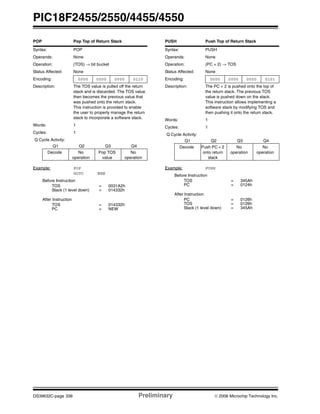
![PIC18F2455/2550/4455/4550
DS39632C-page 326 Preliminary © 2006 Microchip Technology Inc.
DAW Decimal Adjust W Register
Syntax: DAW
Operands: None
Operation: If [W<3:0> > 9] or [DC = 1] then
(W<3:0>) + 6 → W<3:0>;
else
(W<3:0>) → W<3:0>
If [W<7:4> + DC > 9] or [C = 1] then
(W<7:4>) + 6 + DC → W<7:4>;
else
(W<7:4>) + DC → W<7:4>
Status Affected: C
Encoding: 0000 0000 0000 0111
Description: DAW adjusts the eight-bit value in W,
resulting from the earlier addition of two
variables (each in packed BCD format)
and produces a correct packed BCD
result.
Words: 1
Cycles: 1
Q Cycle Activity:
Q1 Q2 Q3 Q4
Decode Read
register W
Process
Data
Write
W
Example 1: DAW
Before Instruction
W = A5h
C = 0
DC = 0
After Instruction
W = 05h
C = 1
DC = 0
Example 2:
Before Instruction
W = CEh
C = 0
DC = 0
After Instruction
W = 34h
C = 1
DC = 0
DECF Decrement f
Syntax: DECF f {,d {,a}}
Operands: 0 ≤ f ≤ 255
d ∈ [0,1]
a ∈ [0,1]
Operation: (f) – 1 → dest
Status Affected: C, DC, N, OV, Z
Encoding: 0000 01da ffff ffff
Description: Decrement register ‘f’. If ‘d’ is ‘0’, the
result is stored in W. If ‘d’ is ‘1’, the
result is stored back in register ‘f’
(default).
If ‘a’ is ‘0’, the Access Bank is selected.
If ‘a’ is ‘1’, the BSR is used to select the
GPR bank (default).
If ‘a’ is ‘0’ and the extended instruction
set is enabled, this instruction operates
in Indexed Literal Offset Addressing
mode whenever f ≤ 95 (5Fh). See
Section 26.2.3 “Byte-Oriented and
Bit-Oriented Instructions in Indexed
Literal Offset Mode” for details.
Words: 1
Cycles: 1
Q Cycle Activity:
Q1 Q2 Q3 Q4
Decode Read
register ‘f’
Process
Data
Write to
destination
Example: DECF CNT, 1, 0
Before Instruction
CNT = 01h
Z = 0
After Instruction
CNT = 00h
Z = 1](https://image.slidesharecdn.com/pic18f4550-140425123621-phpapp01/85/Pic18f4550-328-320.jpg)
![© 2006 Microchip Technology Inc. Preliminary DS39632C-page 327
PIC18F2455/2550/4455/4550
DECFSZ Decrement f, Skip if 0
Syntax: DECFSZ f {,d {,a}}
Operands: 0 ≤ f ≤ 255
d ∈ [0,1]
a ∈ [0,1]
Operation: (f) – 1 → dest,
skip if result = 0
Status Affected: None
Encoding: 0010 11da ffff ffff
Description: The contents of register ‘f’ are
decremented. If ‘d’ is ‘0’, the result is
placed in W. If ‘d’ is ‘1’, the result is
placed back in register ‘f’ (default).
If the result is ‘0’, the next instruction,
which is already fetched, is discarded
and a NOP is executed instead, making
it a two-cycle instruction.
If ‘a’ is ‘0’, the Access Bank is selected.
If ‘a’ is ‘1’, the BSR is used to select the
GPR bank (default).
If ‘a’ is ‘0’ and the extended instruction
set is enabled, this instruction operates
in Indexed Literal Offset Addressing
mode whenever f ≤ 95 (5Fh). See
Section 26.2.3 “Byte-Oriented and
Bit-Oriented Instructions in Indexed
Literal Offset Mode” for details.
Words: 1
Cycles: 1(2)
Note: 3 cycles if skip and followed
by a 2-word instruction.
Q Cycle Activity:
Q1 Q2 Q3 Q4
Decode Read
register ‘f’
Process
Data
Write to
destination
If skip:
Q1 Q2 Q3 Q4
No
operation
No
operation
No
operation
No
operation
If skip and followed by 2-word instruction:
Q1 Q2 Q3 Q4
No
operation
No
operation
No
operation
No
operation
No
operation
No
operation
No
operation
No
operation
Example: HERE DECFSZ CNT, 1, 1
GOTO LOOP
CONTINUE
Before Instruction
PC = Address (HERE)
After Instruction
CNT = CNT – 1
If CNT = 0;
PC = Address (CONTINUE)
If CNT ≠ 0;
PC = Address (HERE + 2)
DCFSNZ Decrement f, Skip if Not 0
Syntax: DCFSNZ f {,d {,a}}
Operands: 0 ≤ f ≤ 255
d ∈ [0,1]
a ∈ [0,1]
Operation: (f) – 1 → dest,
skip if result ≠ 0
Status Affected: None
Encoding: 0100 11da ffff ffff
Description: The contents of register ‘f’ are
decremented. If ‘d’ is ‘0’, the result is
placed in W. If ‘d’ is ‘1’, the result is
placed back in register ‘f’ (default).
If the result is not ‘0’, the next
instruction, which is already fetched, is
discarded and a NOP is executed
instead, making it a two-cycle
instruction.
If ‘a’ is ‘0’, the Access Bank is selected.
If ‘a’ is ‘1’, the BSR is used to select the
GPR bank (default).
If ‘a’ is ‘0’ and the extended instruction
set is enabled, this instruction operates
in Indexed Literal Offset Addressing
mode whenever f ≤ 95 (5Fh). See
Section 26.2.3 “Byte-Oriented and
Bit-Oriented Instructions in Indexed
Literal Offset Mode” for details.
Words: 1
Cycles: 1(2)
Note: 3 cycles if skip and followed
by a 2-word instruction.
Q Cycle Activity:
Q1 Q2 Q3 Q4
Decode Read
register ‘f’
Process
Data
Write to
destination
If skip:
Q1 Q2 Q3 Q4
No
operation
No
operation
No
operation
No
operation
If skip and followed by 2-word instruction:
Q1 Q2 Q3 Q4
No
operation
No
operation
No
operation
No
operation
No
operation
No
operation
No
operation
No
operation
Example: HERE DCFSNZ TEMP, 1, 0
ZERO :
NZERO :
Before Instruction
TEMP = ?
After Instruction
TEMP = TEMP – 1,
If TEMP = 0;
PC = Address (ZERO)
If TEMP ≠ 0;
PC = Address (NZERO)](https://image.slidesharecdn.com/pic18f4550-140425123621-phpapp01/85/Pic18f4550-329-320.jpg)
![PIC18F2455/2550/4455/4550
DS39632C-page 328 Preliminary © 2006 Microchip Technology Inc.
GOTO Unconditional Branch
Syntax: GOTO k
Operands: 0 ≤ k ≤ 1048575
Operation: k → PC<20:1>
Status Affected: None
Encoding:
1st word (k<7:0>)
2nd word(k<19:8>)
1110
1111
1111
k19kkk
k7kkk
kkkk
kkkk0
kkkk8
Description: GOTO allows an unconditional branch
anywhere within the entire
2-Mbyte memory range. The 20-bit
value ‘k’ is loaded into PC<20:1>. GOTO
is always a two-cycle instruction.
Words: 2
Cycles: 2
Q Cycle Activity:
Q1 Q2 Q3 Q4
Decode Read literal
‘k’<7:0>,
No
operation
Read literal
‘k’<19:8>,
Write to PC
No
operation
No
operation
No
operation
No
operation
Example: GOTO THERE
After Instruction
PC = Address (THERE)
INCF Increment f
Syntax: INCF f {,d {,a}}
Operands: 0 ≤ f ≤ 255
d ∈ [0,1]
a ∈ [0,1]
Operation: (f) + 1 → dest
Status Affected: C, DC, N, OV, Z
Encoding: 0010 10da ffff ffff
Description: The contents of register ‘f’ are
incremented. If ‘d’ is ‘0’, the result is
placed in W. If ‘d’ is ‘1’, the result is
placed back in register ‘f’ (default).
If ‘a’ is ‘0’, the Access Bank is selected.
If ‘a’ is ‘1’, the BSR is used to select the
GPR bank (default).
If ‘a’ is ‘0’ and the extended instruction
set is enabled, this instruction operates
in Indexed Literal Offset Addressing
mode whenever f ≤ 95 (5Fh). See
Section 26.2.3 “Byte-Oriented and
Bit-Oriented Instructions in Indexed
Literal Offset Mode” for details.
Words: 1
Cycles: 1
Q Cycle Activity:
Q1 Q2 Q3 Q4
Decode Read
register ‘f’
Process
Data
Write to
destination
Example: INCF CNT, 1, 0
Before Instruction
CNT = FFh
Z = 0
C = ?
DC = ?
After Instruction
CNT = 00h
Z = 1
C = 1
DC = 1](https://image.slidesharecdn.com/pic18f4550-140425123621-phpapp01/85/Pic18f4550-330-320.jpg)
![© 2006 Microchip Technology Inc. Preliminary DS39632C-page 329
PIC18F2455/2550/4455/4550
INCFSZ Increment f, Skip if 0
Syntax: INCFSZ f {,d {,a}}
Operands: 0 ≤ f ≤ 255
d ∈ [0,1]
a ∈ [0,1]
Operation: (f) + 1 → dest,
skip if result = 0
Status Affected: None
Encoding: 0011 11da ffff ffff
Description: The contents of register ‘f’ are
incremented. If ‘d’ is ‘0’, the result is
placed in W. If ‘d’ is ‘1’, the result is
placed back in register ‘f’. (default)
If the result is ‘0’, the next instruction,
which is already fetched, is discarded
and a NOP is executed instead, making
it a two-cycle instruction.
If ‘a’ is ‘0’, the Access Bank is selected.
If ‘a’ is ‘1’, the BSR is used to select the
GPR bank (default).
If ‘a’ is ‘0’ and the extended instruction
set is enabled, this instruction operates
in Indexed Literal Offset Addressing
mode whenever f ≤ 95 (5Fh). See
Section 26.2.3 “Byte-Oriented and
Bit-Oriented Instructions in Indexed
Literal Offset Mode” for details.
Words: 1
Cycles: 1(2)
Note: 3 cycles if skip and followed
by a 2-word instruction.
Q Cycle Activity:
Q1 Q2 Q3 Q4
Decode Read
register ‘f’
Process
Data
Write to
destination
If skip:
Q1 Q2 Q3 Q4
No
operation
No
operation
No
operation
No
operation
If skip and followed by 2-word instruction:
Q1 Q2 Q3 Q4
No
operation
No
operation
No
operation
No
operation
No
operation
No
operation
No
operation
No
operation
Example: HERE INCFSZ CNT, 1, 0
NZERO :
ZERO :
Before Instruction
PC = Address (HERE)
After Instruction
CNT = CNT + 1
If CNT = 0;
PC = Address (ZERO)
If CNT ≠ 0;
PC = Address (NZERO)
INFSNZ Increment f, Skip if Not 0
Syntax: INFSNZ f {,d {,a}}
Operands: 0 ≤ f ≤ 255
d ∈ [0,1]
a ∈ [0,1]
Operation: (f) + 1 → dest,
skip if result ≠ 0
Status Affected: None
Encoding: 0100 10da ffff ffff
Description: The contents of register ‘f’ are
incremented. If ‘d’ is ‘0’, the result is
placed in W. If ‘d’ is ‘1’, the result is
placed back in register ‘f’ (default).
If the result is not ‘0’, the next
instruction, which is already fetched, is
discarded and a NOP is executed
instead, making it a two-cycle
instruction.
If ‘a’ is ‘0’, the Access Bank is selected.
If ‘a’ is ‘1’, the BSR is used to select the
GPR bank (default).
If ‘a’ is ‘0’ and the extended instruction
set is enabled, this instruction operates
in Indexed Literal Offset Addressing
mode whenever f ≤ 95 (5Fh). See
Section 26.2.3 “Byte-Oriented and
Bit-Oriented Instructions in Indexed
Literal Offset Mode” for details.
Words: 1
Cycles: 1(2)
Note: 3 cycles if skip and followed
by a 2-word instruction.
Q Cycle Activity:
Q1 Q2 Q3 Q4
Decode Read
register ‘f’
Process
Data
Write to
destination
If skip:
Q1 Q2 Q3 Q4
No
operation
No
operation
No
operation
No
operation
If skip and followed by 2-word instruction:
Q1 Q2 Q3 Q4
No
operation
No
operation
No
operation
No
operation
No
operation
No
operation
No
operation
No
operation
Example: HERE INFSNZ REG, 1, 0
ZERO
NZERO
Before Instruction
PC = Address (HERE)
After Instruction
REG = REG + 1
If REG ≠ 0;
PC = Address (NZERO)
If REG = 0;
PC = Address (ZERO)](https://image.slidesharecdn.com/pic18f4550-140425123621-phpapp01/85/Pic18f4550-331-320.jpg)
![PIC18F2455/2550/4455/4550
DS39632C-page 330 Preliminary © 2006 Microchip Technology Inc.
IORLW Inclusive OR Literal with W
Syntax: IORLW k
Operands: 0 ≤ k ≤ 255
Operation: (W) .OR. k → W
Status Affected: N, Z
Encoding: 0000 1001 kkkk kkkk
Description: The contents of W are ORed with the
eight-bit literal ‘k’. The result is placed in
W.
Words: 1
Cycles: 1
Q Cycle Activity:
Q1 Q2 Q3 Q4
Decode Read
literal ‘k’
Process
Data
Write to W
Example: IORLW 35h
Before Instruction
W = 9Ah
After Instruction
W = BFh
IORWF Inclusive OR W with f
Syntax: IORWF f {,d {,a}}
Operands: 0 ≤ f ≤ 255
d ∈ [0,1]
a ∈ [0,1]
Operation: (W) .OR. (f) → dest
Status Affected: N, Z
Encoding: 0001 00da ffff ffff
Description: Inclusive OR W with register ‘f’. If ‘d’ is
‘0’, the result is placed in W. If ‘d’ is ‘1’,
the result is placed back in register ‘f’
(default).
If ‘a’ is ‘0’, the Access Bank is selected.
If ‘a’ is ‘1’, the BSR is used to select the
GPR bank (default).
If ‘a’ is ‘0’ and the extended instruction
set is enabled, this instruction operates
in Indexed Literal Offset Addressing
mode whenever f ≤ 95 (5Fh). See
Section 26.2.3 “Byte-Oriented and
Bit-Oriented Instructions in Indexed
Literal Offset Mode” for details.
Words: 1
Cycles: 1
Q Cycle Activity:
Q1 Q2 Q3 Q4
Decode Read
register ‘f’
Process
Data
Write to
destination
Example: IORWF RESULT, 0, 1
Before Instruction
RESULT = 13h
W = 91h
After Instruction
RESULT = 13h
W = 93h](https://image.slidesharecdn.com/pic18f4550-140425123621-phpapp01/85/Pic18f4550-332-320.jpg)
![© 2006 Microchip Technology Inc. Preliminary DS39632C-page 331
PIC18F2455/2550/4455/4550
LFSR Load FSR
Syntax: LFSR f, k
Operands: 0 ≤ f ≤ 2
0 ≤ k ≤ 4095
Operation: k → FSRf
Status Affected: None
Encoding: 1110
1111
1110
0000
00ff
k7kkk
k11kkk
kkkk
Description: The 12-bit literal ‘k’ is loaded into the
File Select Register pointed to by ‘f’.
Words: 2
Cycles: 2
Q Cycle Activity:
Q1 Q2 Q3 Q4
Decode Read literal
‘k’ MSB
Process
Data
Write
literal ‘k’ MSB
to FSRfH
Decode Read literal
‘k’ LSB
Process
Data
Write literal ‘k’
to FSRfL
Example: LFSR 2, 3ABh
After Instruction
FSR2H = 03h
FSR2L = ABh
MOVF Move f
Syntax: MOVF f {,d {,a}}
Operands: 0 ≤ f ≤ 255
d ∈ [0,1]
a ∈ [0,1]
Operation: f → dest
Status Affected: N, Z
Encoding: 0101 00da ffff ffff
Description: The contents of register ‘f’ are moved to
a destination dependent upon the
status of ‘d’. If ‘d’ is ‘0’, the result is
placed in W. If ‘d’ is ‘1’, the result is
placed back in register ‘f’ (default).
Location ‘f’ can be anywhere in the
256-byte bank.
If ‘a’ is ‘0’, the Access Bank is selected.
If ‘a’ is ‘1’, the BSR is used to select the
GPR bank (default).
If ‘a’ is ‘0’ and the extended instruction
set is enabled, this instruction operates
in Indexed Literal Offset Addressing
mode whenever f ≤ 95 (5Fh). See
Section 26.2.3 “Byte-Oriented and
Bit-Oriented Instructions in Indexed
Literal Offset Mode” for details.
Words: 1
Cycles: 1
Q Cycle Activity:
Q1 Q2 Q3 Q4
Decode Read
register ‘f’
Process
Data
Write W
Example: MOVF REG, 0, 0
Before Instruction
REG = 22h
W = FFh
After Instruction
REG = 22h
W = 22h](https://image.slidesharecdn.com/pic18f4550-140425123621-phpapp01/85/Pic18f4550-333-320.jpg)
![© 2006 Microchip Technology Inc. Preliminary DS39632C-page 333
PIC18F2455/2550/4455/4550
MOVLW Move Literal to W
Syntax: MOVLW k
Operands: 0 ≤ k ≤ 255
Operation: k → W
Status Affected: None
Encoding: 0000 1110 kkkk kkkk
Description: The eight-bit literal ‘k’ is loaded into W.
Words: 1
Cycles: 1
Q Cycle Activity:
Q1 Q2 Q3 Q4
Decode Read
literal ‘k’
Process
Data
Write to W
Example: MOVLW 5Ah
After Instruction
W = 5Ah
MOVWF Move W to f
Syntax: MOVWF f {,a}
Operands: 0 ≤ f ≤ 255
a ∈ [0,1]
Operation: (W) → f
Status Affected: None
Encoding: 0110 111a ffff ffff
Description: Move data from W to register ‘f’.
Location ‘f’ can be anywhere in the
256-byte bank.
If ‘a’ is ‘0’, the Access Bank is selected.
If ‘a’ is ‘1’, the BSR is used to select the
GPR bank (default).
If ‘a’ is ‘0’ and the extended instruction
set is enabled, this instruction operates
in Indexed Literal Offset Addressing
mode whenever f ≤ 95 (5Fh). See
Section 26.2.3 “Byte-Oriented and
Bit-Oriented Instructions in Indexed
Literal Offset Mode” for details.
Words: 1
Cycles: 1
Q Cycle Activity:
Q1 Q2 Q3 Q4
Decode Read
register ‘f’
Process
Data
Write
register ‘f’
Example: MOVWF REG, 0
Before Instruction
W = 4Fh
REG = FFh
After Instruction
W = 4Fh
REG = 4Fh](https://image.slidesharecdn.com/pic18f4550-140425123621-phpapp01/85/Pic18f4550-335-320.jpg)
![PIC18F2455/2550/4455/4550
DS39632C-page 334 Preliminary © 2006 Microchip Technology Inc.
MULLW Multiply Literal with W
Syntax: MULLW k
Operands: 0 ≤ k ≤ 255
Operation: (W) x k → PRODH:PRODL
Status Affected: None
Encoding: 0000 1101 kkkk kkkk
Description: An unsigned multiplication is carried
out between the contents of W and the
8-bit literal ‘k’. The 16-bit result is
placed in PRODH:PRODL register pair.
PRODH contains the high byte.
W is unchanged.
None of the Status flags are affected.
Note that neither Overflow nor Carry is
possible in this operation. A zero result
is possible but not detected.
Words: 1
Cycles: 1
Q Cycle Activity:
Q1 Q2 Q3 Q4
Decode Read
literal ‘k’
Process
Data
Write
registers
PRODH:
PRODL
Example: MULLW 0C4h
Before Instruction
W = E2h
PRODH = ?
PRODL = ?
After Instruction
W = E2h
PRODH = ADh
PRODL = 08h
MULWF Multiply W with f
Syntax: MULWF f {,a}
Operands: 0 ≤ f ≤ 255
a ∈ [0,1]
Operation: (W) x (f) → PRODH:PRODL
Status Affected: None
Encoding: 0000 001a ffff ffff
Description: An unsigned multiplication is carried
out between the contents of W and the
register file location ‘f’. The 16-bit
result is stored in the PRODH:PRODL
register pair. PRODH contains the
high byte. Both W and ‘f’ are
unchanged.
None of the Status flags are affected.
Note that neither Overflow nor Carry is
possible in this operation. A zero
result is possible but not detected.
If ‘a’ is ‘0’, the Access Bank is
selected. If ‘a’ is ‘1’, the BSR is used
to select the GPR bank (default).
If ‘a’ is ‘0’ and the extended instruction
set is enabled, this instruction
operates in Indexed Literal Offset
Addressing mode whenever
f ≤ 95 (5Fh). See Section 26.2.3
“Byte-Oriented and Bit-Oriented
Instructions in Indexed Literal Offset
Mode” for details.
Words: 1
Cycles: 1
Q Cycle Activity:
Q1 Q2 Q3 Q4
Decode Read
register ‘f’
Process
Data
Write
registers
PRODH:
PRODL
Example: MULWF REG, 1
Before Instruction
W = C4h
REG = B5h
PRODH = ?
PRODL = ?
After Instruction
W = C4h
REG = B5h
PRODH = 8Ah
PRODL = 94h](https://image.slidesharecdn.com/pic18f4550-140425123621-phpapp01/85/Pic18f4550-336-320.jpg)
![© 2006 Microchip Technology Inc. Preliminary DS39632C-page 335
PIC18F2455/2550/4455/4550
NEGF Negate f
Syntax: NEGF f {,a}
Operands: 0 ≤ f ≤ 255
a ∈ [0,1]
Operation: (f) + 1 → f
Status Affected: N, OV, C, DC, Z
Encoding: 0110 110a ffff ffff
Description: Location ‘f’ is negated using two’s
complement. The result is placed in the
data memory location ‘f’.
If ‘a’ is ‘0’, the Access Bank is selected.
If ‘a’ is ‘1’, the BSR is used to select the
GPR bank (default).
If ‘a’ is ‘0’ and the extended instruction
set is enabled, this instruction operates
in Indexed Literal Offset Addressing
mode whenever f ≤ 95 (5Fh). See
Section 26.2.3 “Byte-Oriented and
Bit-Oriented Instructions in Indexed
Literal Offset Mode” for details.
Words: 1
Cycles: 1
Q Cycle Activity:
Q1 Q2 Q3 Q4
Decode Read
register ‘f’
Process
Data
Write
register ‘f’
Example: NEGF REG, 1
Before Instruction
REG = 0011 1010 [3Ah]
After Instruction
REG = 1100 0110 [C6h]
NOP No Operation
Syntax: NOP
Operands: None
Operation: No operation
Status Affected: None
Encoding: 0000
1111
0000
xxxx
0000
xxxx
0000
xxxx
Description: No operation.
Words: 1
Cycles: 1
Q Cycle Activity:
Q1 Q2 Q3 Q4
Decode No
operation
No
operation
No
operation
Example:
None.](https://image.slidesharecdn.com/pic18f4550-140425123621-phpapp01/85/Pic18f4550-337-320.jpg)
![PIC18F2455/2550/4455/4550
DS39632C-page 338 Preliminary © 2006 Microchip Technology Inc.
RETFIE Return from Interrupt
Syntax: RETFIE {s}
Operands: s ∈ [0,1]
Operation: (TOS) → PC,
1 → GIE/GIEH or PEIE/GIEL,
if s = 1
(WS) → W,
(STATUSS) → STATUS,
(BSRS) → BSR,
PCLATU, PCLATH are unchanged
Status Affected: GIE/GIEH, PEIE/GIEL.
Encoding: 0000 0000 0001 000s
Description: Return from interrupt. Stack is popped
and Top-of-Stack (TOS) is loaded into
the PC. Interrupts are enabled by
setting either the high or low priority
global interrupt enable bit. If ‘s’ = 1, the
contents of the shadow registers WS,
STATUSS and BSRS are loaded into
their corresponding registers, W,
STATUS and BSR. If ‘s’ = 0, no update
of these registers occurs (default).
Words: 1
Cycles: 2
Q Cycle Activity:
Q1 Q2 Q3 Q4
Decode No
operation
No
operation
Pop PC from
stack
Set GIEH or
GIEL
No
operation
No
operation
No
operation
No
operation
Example: RETFIE 1
After Interrupt
PC = TOS
W = WS
BSR = BSRS
STATUS = STATUSS
GIE/GIEH, PEIE/GIEL = 1
RETLW Return Literal to W
Syntax: RETLW k
Operands: 0 ≤ k ≤ 255
Operation: k → W,
(TOS) → PC,
PCLATU, PCLATH are unchanged
Status Affected: None
Encoding: 0000 1100 kkkk kkkk
Description: W is loaded with the eight-bit literal ‘k’.
The program counter is loaded from the
top of the stack (the return address).
The high address latch (PCLATH)
remains unchanged.
Words: 1
Cycles: 2
Q Cycle Activity:
Q1 Q2 Q3 Q4
Decode Read
literal ‘k’
Process
Data
Pop PC from
stack, Write
to W
No
operation
No
operation
No
operation
No
operation
Example:
CALL TABLE ; W contains table
; offset value
; W now has
; table value
:
TABLE
ADDWF PCL ; W = offset
RETLW k0 ; Begin table
RETLW k1 ;
:
:
RETLW kn ; End of table
Before Instruction
W = 07h
After Instruction
W = value of kn](https://image.slidesharecdn.com/pic18f4550-140425123621-phpapp01/85/Pic18f4550-340-320.jpg)
![© 2006 Microchip Technology Inc. Preliminary DS39632C-page 339
PIC18F2455/2550/4455/4550
RETURN Return from Subroutine
Syntax: RETURN {s}
Operands: s ∈ [0,1]
Operation: (TOS) → PC,
if s = 1
(WS) → W,
(STATUSS) → STATUS,
(BSRS) → BSR,
PCLATU, PCLATH are unchanged
Status Affected: None
Encoding: 0000 0000 0001 001s
Description: Return from subroutine. The stack is
popped and the top of the stack (TOS)
is loaded into the program counter. If
‘s’= 1, the contents of the shadow
registers WS, STATUSS and BSRS are
loaded into their corresponding
registers, W, STATUS and BSR. If
‘s’ = 0, no update of these registers
occurs (default).
Words: 1
Cycles: 2
Q Cycle Activity:
Q1 Q2 Q3 Q4
Decode No
operation
Process
Data
Pop PC
from stack
No
operation
No
operation
No
operation
No
operation
Example: RETURN
After Instruction:
PC = TOS
RLCF Rotate Left f through Carry
Syntax: RLCF f {,d {,a}}
Operands: 0 ≤ f ≤ 255
d ∈ [0,1]
a ∈ [0,1]
Operation: (f<n>) → dest<n + 1>,
(f<7>) → C,
(C) → dest<0>
Status Affected: C, N, Z
Encoding: 0011 01da ffff ffff
Description: The contents of register ‘f’ are rotated
one bit to the left through the Carry
flag. If ‘d’ is ‘0’, the result is placed in
W. If ‘d’ is ‘1’, the result is stored back
in register ‘f’ (default).
If ‘a’ is ‘0’, the Access Bank is
selected. If ‘a’ is ‘1’, the BSR is used to
select the GPR bank (default).
If ‘a’ is ‘0’ and the extended instruction
set is enabled, this instruction
operates in Indexed Literal Offset
Addressing mode whenever
f ≤ 95 (5Fh). See Section 26.2.3
“Byte-Oriented and Bit-Oriented
Instructions in Indexed Literal Offset
Mode” for details.
Words: 1
Cycles: 1
Q Cycle Activity:
Q1 Q2 Q3 Q4
Decode Read
register ‘f’
Process
Data
Write to
destination
Example: RLCF REG, 0, 0
Before Instruction
REG = 1110 0110
C = 0
After Instruction
REG = 1110 0110
W = 1100 1100
C = 1
C register f](https://image.slidesharecdn.com/pic18f4550-140425123621-phpapp01/85/Pic18f4550-341-320.jpg)
![PIC18F2455/2550/4455/4550
DS39632C-page 340 Preliminary © 2006 Microchip Technology Inc.
RLNCF Rotate Left f (No Carry)
Syntax: RLNCF f {,d {,a}}
Operands: 0 ≤ f ≤ 255
d ∈ [0,1]
a ∈ [0,1]
Operation: (f<n>) → dest<n + 1>,
(f<7>) → dest<0>
Status Affected: N, Z
Encoding: 0100 01da ffff ffff
Description: The contents of register ‘f’ are rotated
one bit to the left. If ‘d’ is ‘0’, the result
is placed in W. If ‘d’ is ‘1’, the result is
stored back in register ‘f’ (default).
If ‘a’ is ‘0’, the Access Bank is selected.
If ‘a’ is ‘1’, the BSR is used to select the
GPR bank (default).
If ‘a’ is ‘0’ and the extended instruction
set is enabled, this instruction operates
in Indexed Literal Offset Addressing
mode whenever f ≤ 95 (5Fh). See
Section 26.2.3 “Byte-Oriented and
Bit-Oriented Instructions in Indexed
Literal Offset Mode” for details.
Words: 1
Cycles: 1
Q Cycle Activity:
Q1 Q2 Q3 Q4
Decode Read
register ‘f’
Process
Data
Write to
destination
Example: RLNCF REG, 1, 0
Before Instruction
REG = 1010 1011
After Instruction
REG = 0101 0111
register f
RRCF Rotate Right f through Carry
Syntax: RRCF f {,d {,a}}
Operands: 0 ≤ f ≤ 255
d ∈ [0,1]
a ∈ [0,1]
Operation: (f<n>) → dest<n – 1>,
(f<0>) → C,
(C) → dest<7>
Status Affected: C, N, Z
Encoding: 0011 00da ffff ffff
Description: The contents of register ‘f’ are rotated
one bit to the right through the Carry
flag. If ‘d’ is ‘0’, the result is placed in W.
If ‘d’ is ‘1’, the result is placed back in
register ‘f’ (default).
If ‘a’ is ‘0’, the Access Bank is selected.
If ‘a’ is ‘1’, the BSR is used to select the
GPR bank (default).
If ‘a’ is ‘0’ and the extended instruction
set is enabled, this instruction operates
in Indexed Literal Offset Addressing
mode whenever f ≤ 95 (5Fh). See
Section 26.2.3 “Byte-Oriented and
Bit-Oriented Instructions in Indexed
Literal Offset Mode” for details.
Words: 1
Cycles: 1
Q Cycle Activity:
Q1 Q2 Q3 Q4
Decode Read
register ‘f’
Process
Data
Write to
destination
Example: RRCF REG, 0, 0
Before Instruction
REG = 1110 0110
C = 0
After Instruction
REG = 1110 0110
W = 0111 0011
C = 0
C register f](https://image.slidesharecdn.com/pic18f4550-140425123621-phpapp01/85/Pic18f4550-342-320.jpg)
![© 2006 Microchip Technology Inc. Preliminary DS39632C-page 341
PIC18F2455/2550/4455/4550
RRNCF Rotate Right f (No Carry)
Syntax: RRNCF f {,d {,a}}
Operands: 0 ≤ f ≤ 255
d ∈ [0,1]
a ∈ [0,1]
Operation: (f<n>) → dest<n – 1>,
(f<0>) → dest<7>
Status Affected: N, Z
Encoding: 0100 00da ffff ffff
Description: The contents of register ‘f’ are rotated
one bit to the right. If ‘d’ is ‘0’, the result
is placed in W. If ‘d’ is ‘1’, the result is
placed back in register ‘f’ (default).
If ‘a’ is ‘0’, the Access Bank will be
selected, overriding the BSR value. If ‘a’
is ‘1’, then the bank will be selected as
per the BSR value (default).
If ‘a’ is ‘0’ and the extended instruction
set is enabled, this instruction operates
in Indexed Literal Offset Addressing
mode whenever f ≤ 95 (5Fh). See
Section 26.2.3 “Byte-Oriented and
Bit-Oriented Instructions in Indexed
Literal Offset Mode” for details.
Words: 1
Cycles: 1
Q Cycle Activity:
Q1 Q2 Q3 Q4
Decode Read
register ‘f’
Process
Data
Write to
destination
Example 1: RRNCF REG, 1, 0
Before Instruction
REG = 1101 0111
After Instruction
REG = 1110 1011
Example 2: RRNCF REG, 0, 0
Before Instruction
W = ?
REG = 1101 0111
After Instruction
W = 1110 1011
REG = 1101 0111
register f
SETF Set f
Syntax: SETF f {,a}
Operands: 0 ≤ f ≤ 255
a ∈ [0,1]
Operation: FFh → f
Status Affected: None
Encoding: 0110 100a ffff ffff
Description: The contents of the specified register
are set to FFh.
If ‘a’ is ‘0’, the Access Bank is selected.
If ‘a’ is ‘1’, the BSR is used to select the
GPR bank (default).
If ‘a’ is ‘0’ and the extended instruction
set is enabled, this instruction operates
in Indexed Literal Offset Addressing
mode whenever f ≤ 95 (5Fh). See
Section 26.2.3 “Byte-Oriented and
Bit-Oriented Instructions in Indexed
Literal Offset Mode” for details.
Words: 1
Cycles: 1
Q Cycle Activity:
Q1 Q2 Q3 Q4
Decode Read
register ‘f’
Process
Data
Write
register ‘f’
Example: SETF REG,1
Before Instruction
REG = 5Ah
After Instruction
REG = FFh](https://image.slidesharecdn.com/pic18f4550-140425123621-phpapp01/85/Pic18f4550-343-320.jpg)
![PIC18F2455/2550/4455/4550
DS39632C-page 342 Preliminary © 2006 Microchip Technology Inc.
SLEEP Enter Sleep mode
Syntax: SLEEP
Operands: None
Operation: 00h → WDT,
0 → WDT postscaler,
1 → TO,
0 → PD
Status Affected: TO, PD
Encoding: 0000 0000 0000 0011
Description: The Power-Down status bit (PD) is
cleared. The Time-out status bit (TO)
is set. Watchdog Timer and its
postscaler are cleared.
The processor is put into Sleep mode
with the oscillator stopped.
Words: 1
Cycles: 1
Q Cycle Activity:
Q1 Q2 Q3 Q4
Decode No
operation
Process
Data
Go to
Sleep
Example: SLEEP
Before Instruction
TO = ?
PD = ?
After Instruction
TO = 1 †
PD = 0
† If WDT causes wake-up, this bit is cleared.
SUBFWB Subtract f from W with Borrow
Syntax: SUBFWB f {,d {,a}}
Operands: 0 ≤ f ≤ 255
d ∈ [0,1]
a ∈ [0,1]
Operation: (W) – (f) – (C) → dest
Status Affected: N, OV, C, DC, Z
Encoding: 0101 01da ffff ffff
Description: Subtract register ‘f’ and Carry flag
(borrow) from W (2’s complement
method). If ‘d’ is ‘0’, the result is stored
in W. If ‘d’ is ‘1’, the result is stored in
register ‘f’ (default).
If ‘a’ is ‘0’, the Access Bank is
selected. If ‘a’ is ‘1’, the BSR is used
to select the GPR bank (default).
If ‘a’ is ‘0’ and the extended instruction
set is enabled, this instruction
operates in Indexed Literal Offset
Addressing mode whenever
f ≤ 95 (5Fh). See Section 26.2.3
“Byte-Oriented and Bit-Oriented
Instructions in Indexed Literal Offset
Mode” for details.
Words: 1
Cycles: 1
Q Cycle Activity:
Q1 Q2 Q3 Q4
Decode Read
register ‘f’
Process
Data
Write to
destination
Example 1: SUBFWB REG, 1, 0
Before Instruction
REG = 3
W = 2
C = 1
After Instruction
REG = FF
W = 2
C = 0
Z = 0
N = 1 ; result is negative
Example 2: SUBFWB REG, 0, 0
Before Instruction
REG = 2
W = 5
C = 1
After Instruction
REG = 2
W = 3
C = 1
Z = 0
N = 0 ; result is positive
Example 3: SUBFWB REG, 1, 0
Before Instruction
REG = 1
W = 2
C = 0
After Instruction
REG = 0
W = 2
C = 1
Z = 1 ; result is zero
N = 0](https://image.slidesharecdn.com/pic18f4550-140425123621-phpapp01/85/Pic18f4550-344-320.jpg)
![© 2006 Microchip Technology Inc. Preliminary DS39632C-page 343
PIC18F2455/2550/4455/4550
SUBLW Subtract W from Literal
Syntax: SUBLW k
Operands: 0 ≤ k ≤ 255
Operation: k – (W) → W
Status Affected: N, OV, C, DC, Z
Encoding: 0000 1000 kkkk kkkk
Description W is subtracted from the eight-bit
literal ‘k’. The result is placed in W.
Words: 1
Cycles: 1
Q Cycle Activity:
Q1 Q2 Q3 Q4
Decode Read
literal ‘k’
Process
Data
Write to W
Example 1: SUBLW 02h
Before Instruction
W = 01h
C = ?
After Instruction
W = 01h
C = 1 ; result is positive
Z = 0
N = 0
Example 2: SUBLW 02h
Before Instruction
W = 02h
C = ?
After Instruction
W = 00h
C = 1 ; result is zero
Z = 1
N = 0
Example 3: SUBLW 02h
Before Instruction
W = 03h
C = ?
After Instruction
W = FFh ; (2’s complement)
C = 0 ; result is negative
Z = 0
N = 1
SUBWF Subtract W from f
Syntax: SUBWF f {,d {,a}}
Operands: 0 ≤ f ≤ 255
d ∈ [0,1]
a ∈ [0,1]
Operation: (f) – (W) → dest
Status Affected: N, OV, C, DC, Z
Encoding: 0101 11da ffff ffff
Description: Subtract W from register ‘f’ (2’s
complement method). If ‘d’ is ‘0’, the
result is stored in W. If ‘d’ is ‘1’, the
result is stored back in register ‘f’
(default).
If ‘a’ is ‘0’, the Access Bank is
selected. If ‘a’ is ‘1’, the BSR is used
to select the GPR bank (default).
If ‘a’ is ‘0’ and the extended instruction
set is enabled, this instruction
operates in Indexed Literal Offset
Addressing mode whenever
f ≤ 95 (5Fh). See Section 26.2.3
“Byte-Oriented and Bit-Oriented
Instructions in Indexed Literal Offset
Mode” for details.
Words: 1
Cycles: 1
Q Cycle Activity:
Q1 Q2 Q3 Q4
Decode Read
register ‘f’
Process
Data
Write to
destination
Example 1: SUBWF REG, 1, 0
Before Instruction
REG = 3
W = 2
C = ?
After Instruction
REG = 1
W = 2
C = 1 ; result is positive
Z = 0
N = 0
Example 2: SUBWF REG, 0, 0
Before Instruction
REG = 2
W = 2
C = ?
After Instruction
REG = 2
W = 0
C = 1 ; result is zero
Z = 1
N = 0
Example 3: SUBWF REG, 1, 0
Before Instruction
REG = 1
W = 2
C = ?
After Instruction
REG = FFh ;(2’s complement)
W = 2
C = 0 ; result is negative
Z = 0
N = 1](https://image.slidesharecdn.com/pic18f4550-140425123621-phpapp01/85/Pic18f4550-345-320.jpg)
![PIC18F2455/2550/4455/4550
DS39632C-page 344 Preliminary © 2006 Microchip Technology Inc.
SUBWFB Subtract W from f with Borrow
Syntax: SUBWFB f {,d {,a}}
Operands: 0 ≤ f ≤ 255
d ∈ [0,1]
a ∈ [0,1]
Operation: (f) – (W) – (C) → dest
Status Affected: N, OV, C, DC, Z
Encoding: 0101 10da ffff ffff
Description: Subtract W and the Carry flag (borrow)
from register ‘f’ (2’s complement
method). If ‘d’ is ‘0’, the result is stored
in W. If ‘d’ is ‘1’, the result is stored back
in register ‘f’ (default).
If ‘a’ is ‘0’, the Access Bank is selected.
If ‘a’ is ‘1’, the BSR is used to select the
GPR bank (default).
If ‘a’ is ‘0’ and the extended instruction
set is enabled, this instruction operates
in Indexed Literal Offset Addressing
mode whenever f ≤ 95 (5Fh). See
Section 26.2.3 “Byte-Oriented and
Bit-Oriented Instructions in Indexed
Literal Offset Mode” for details.
Words: 1
Cycles: 1
Q Cycle Activity:
Q1 Q2 Q3 Q4
Decode Read
register ‘f’
Process
Data
Write to
destination
Example 1: SUBWFB REG, 1, 0
Before Instruction
REG = 19h (0001 1001)
W = 0Dh (0000 1101)
C = 1
After Instruction
REG = 0Ch (0000 1011)
W = 0Dh (0000 1101)
C = 1
Z = 0
N = 0 ; result is positive
Example 2: SUBWFB REG, 0, 0
Before Instruction
REG = 1Bh (0001 1011)
W = 1Ah (0001 1010)
C = 0
After Instruction
REG = 1Bh (0001 1011)
W = 00h
C = 1
Z = 1 ; result is zero
N = 0
Example 3: SUBWFB REG, 1, 0
Before Instruction
REG = 03h (0000 0011)
W = 0Eh (0000 1101)
C = 1
After Instruction
REG = F5h (1111 0100)
; [2’s comp]
W = 0Eh (0000 1101)
C = 0
Z = 0
N = 1 ; result is negative
SWAPF Swap f
Syntax: SWAPF f {,d {,a}}
Operands: 0 ≤ f ≤ 255
d ∈ [0,1]
a ∈ [0,1]
Operation: (f<3:0>) → dest<7:4>,
(f<7:4>) → dest<3:0>
Status Affected: None
Encoding: 0011 10da ffff ffff
Description: The upper and lower nibbles of register
‘f’ are exchanged. If ‘d’ is ‘0’, the result
is placed in W. If ‘d’ is ‘1’, the result is
placed in register ‘f’ (default).
If ‘a’ is ‘0’, the Access Bank is selected.
If ‘a’ is ‘1’, the BSR is used to select the
GPR bank (default).
If ‘a’ is ‘0’ and the extended instruction
set is enabled, this instruction operates
in Indexed Literal Offset Addressing
mode whenever f ≤ 95 (5Fh). See
Section 26.2.3 “Byte-Oriented and
Bit-Oriented Instructions in Indexed
Literal Offset Mode” for details.
Words: 1
Cycles: 1
Q Cycle Activity:
Q1 Q2 Q3 Q4
Decode Read
register ‘f’
Process
Data
Write to
destination
Example: SWAPF REG, 1, 0
Before Instruction
REG = 53h
After Instruction
REG = 35h](https://image.slidesharecdn.com/pic18f4550-140425123621-phpapp01/85/Pic18f4550-346-320.jpg)
![© 2006 Microchip Technology Inc. Preliminary DS39632C-page 345
PIC18F2455/2550/4455/4550
TBLRD Table Read
Syntax: TBLRD ( *; *+; *-; +*)
Operands: None
Operation: if TBLRD *
(Prog Mem (TBLPTR)) → TABLAT;
TBLPTR – No Change;
if TBLRD *+
(Prog Mem (TBLPTR)) → TABLAT;
(TBLPTR) + 1 → TBLPTR;
if TBLRD *-
(Prog Mem (TBLPTR)) → TABLAT;
(TBLPTR) – 1 → TBLPTR;
if TBLRD +*
(TBLPTR) + 1 → TBLPTR;
(Prog Mem (TBLPTR)) → TABLAT
Status Affected: None
Encoding: 0000 0000 0000 10nn
nn=0 *
=1 *+
=2 *-
=3 +*
Description: This instruction is used to read the contents
of Program Memory (P.M.). To address the
program memory, a pointer called Table
Pointer (TBLPTR) is used.
The TBLPTR (a 21-bit pointer) points to
each byte in the program memory. TBLPTR
has a 2-Mbyte address range.
TBLPTR[0] = 0: LeastSignificantByte
of Program Memory
Word
TBLPTR[0] = 1: Most Significant Byte
of Program Memory
Word
The TBLRD instruction can modify the value
of TBLPTR as follows:
• no change
• post-increment
• post-decrement
• pre-increment
Words: 1
Cycles: 2
Q Cycle Activity:
Q1 Q2 Q3 Q4
Decode No
operation
No
operation
No
operation
No
operation
No operation
(Read Program
Memory)
No
operation
No operation
(Write
TABLAT)
TBLRD Table Read (Continued)
Example 1: TBLRD *+ ;
Before Instruction
TABLAT = 55h
TBLPTR = 00A356h
MEMORY (00A356h) = 34h
After Instruction
TABLAT = 34h
TBLPTR = 00A357h
Example 2: TBLRD +* ;
Before Instruction
TABLAT = AAh
TBLPTR = 01A357h
MEMORY (01A357h) = 12h
MEMORY (01A358h) = 34h
After Instruction
TABLAT = 34h
TBLPTR = 01A358h](https://image.slidesharecdn.com/pic18f4550-140425123621-phpapp01/85/Pic18f4550-347-320.jpg)
![PIC18F2455/2550/4455/4550
DS39632C-page 346 Preliminary © 2006 Microchip Technology Inc.
TBLWT Table Write
Syntax: TBLWT ( *; *+; *-; +*)
Operands: None
Operation: if TBLWT*
(TABLAT) → Holding Register;
TBLPTR – No Change;
if TBLWT*+
(TABLAT) → Holding Register;
(TBLPTR) + 1 → TBLPTR;
if TBLWT*-
(TABLAT) → Holding Register;
(TBLPTR) – 1 → TBLPTR;
if TBLWT+*
(TBLPTR) + 1 → TBLPTR;
(TABLAT) → Holding Register
Status Affected: None
Encoding: 0000 0000 0000 11nn
nn=0 *
=1 *+
=2 *-
=3 +*
Description: This instruction uses the 3 LSBs of TBLPTR
to determine which of the
8 holding registers the TABLAT is written to.
The holding registers are used to
program the contents of Program
Memory (P.M.). (Refer to Section 6.0
“Flash Program Memory” for additional
details on programming Flash memory.)
The TBLPTR (a 21-bit pointer) points to
each byte in the program memory. TBLPTR
has a 2-Mbyte address range. The LSb of
the TBLPTR selects which byte of the
program memory location to access.
TBLPTR[0] = 0: Least Significant
Byte of Program
Memory Word
TBLPTR[0] = 1: Most Significant
Byte of Program
Memory Word
The TBLWT instruction can modify the
value of TBLPTR as follows:
• no change
• post-increment
• post-decrement
• pre-increment
Words: 1
Cycles: 2
Q Cycle Activity:
Q1 Q2 Q3 Q4
Decode No
operation
No
operation
No
operation
No
operation
No
operation
(Read
TABLAT)
No
operation
No
operation
(Write to
Holding
Register)
TBLWT Table Write (Continued)
Example 1: TBLWT *+;
Before Instruction
TABLAT = 55h
TBLPTR = 00A356h
HOLDING REGISTER
(00A356h) = FFh
After Instructions (table write completion)
TABLAT = 55h
TBLPTR = 00A357h
HOLDING REGISTER
(00A356h) = 55h
Example 2: TBLWT +*;
Before Instruction
TABLAT = 34h
TBLPTR = 01389Ah
HOLDING REGISTER
(01389Ah) = FFh
HOLDING REGISTER
(01389Bh) = FFh
After Instruction (table write completion)
TABLAT = 34h
TBLPTR = 01389Bh
HOLDING REGISTER
(01389Ah) = FFh
HOLDING REGISTER
(01389Bh) = 34h](https://image.slidesharecdn.com/pic18f4550-140425123621-phpapp01/85/Pic18f4550-348-320.jpg)
![© 2006 Microchip Technology Inc. Preliminary DS39632C-page 347
PIC18F2455/2550/4455/4550
TSTFSZ Test f, Skip if 0
Syntax: TSTFSZ f {,a}
Operands: 0 ≤ f ≤ 255
a ∈ [0,1]
Operation: skip if f = 0
Status Affected: None
Encoding: 0110 011a ffff ffff
Description: If ‘f’ = 0, the next instruction fetched
during the current instruction execution
is discarded and a NOP is executed,
making this a two-cycle instruction.
If ‘a’ is ‘0’, the Access Bank is selected.
If ‘a’ is ‘1’, the BSR is used to select the
GPR bank (default).
If ‘a’ is ‘0’ and the extended instruction
set is enabled, this instruction operates
in Indexed Literal Offset Addressing
mode whenever f ≤ 95 (5Fh). See
Section 26.2.3 “Byte-Oriented and
Bit-Oriented Instructions in Indexed
Literal Offset Mode” for details.
Words: 1
Cycles: 1(2)
Note: 3 cycles if skip and followed
by a 2-word instruction.
Q Cycle Activity:
Q1 Q2 Q3 Q4
Decode Read
register ‘f’
Process
Data
No
operation
If skip:
Q1 Q2 Q3 Q4
No
operation
No
operation
No
operation
No
operation
If skip and followed by 2-word instruction:
Q1 Q2 Q3 Q4
No
operation
No
operation
No
operation
No
operation
No
operation
No
operation
No
operation
No
operation
Example: HERE TSTFSZ CNT, 1
NZERO :
ZERO :
Before Instruction
PC = Address (HERE)
After Instruction
If CNT = 00h,
PC = Address (ZERO)
If CNT ≠ 00h,
PC = Address (NZERO)
XORLW Exclusive OR Literal with W
Syntax: XORLW k
Operands: 0 ≤ k ≤ 255
Operation: (W) .XOR. k → W
Status Affected: N, Z
Encoding: 0000 1010 kkkk kkkk
Description: The contents of W are XORed with
the 8-bit literal ‘k’. The result is placed
in W.
Words: 1
Cycles: 1
Q Cycle Activity:
Q1 Q2 Q3 Q4
Decode Read
literal ‘k’
Process
Data
Write to W
Example: XORLW 0AFh
Before Instruction
W = B5h
After Instruction
W = 1Ah](https://image.slidesharecdn.com/pic18f4550-140425123621-phpapp01/85/Pic18f4550-349-320.jpg)
![PIC18F2455/2550/4455/4550
DS39632C-page 348 Preliminary © 2006 Microchip Technology Inc.
XORWF Exclusive OR W with f
Syntax: XORWF f {,d {,a}}
Operands: 0 ≤ f ≤ 255
d ∈ [0,1]
a ∈ [0,1]
Operation: (W) .XOR. (f) → dest
Status Affected: N, Z
Encoding: 0001 10da ffff ffff
Description: Exclusive OR the contents of W with
register ‘f’. If ‘d’ is ‘0’, the result is stored
in W. If ‘d’ is ‘1’, the result is stored back
in the register ‘f’ (default).
If ‘a’ is ‘0’, the Access Bank is selected.
If ‘a’ is ‘1’, the BSR is used to select the
GPR bank (default).
If ‘a’ is ‘0’ and the extended instruction
set is enabled, this instruction operates
in Indexed Literal Offset Addressing
mode whenever f ≤ 95 (5Fh). See
Section 26.2.3 “Byte-Oriented and
Bit-Oriented Instructions in Indexed
Literal Offset Mode” for details.
Words: 1
Cycles: 1
Q Cycle Activity:
Q1 Q2 Q3 Q4
Decode Read
register ‘f’
Process
Data
Write to
destination
Example: XORWF REG, 1, 0
Before Instruction
REG = AFh
W = B5h
After Instruction
REG = 1Ah
W = B5h](https://image.slidesharecdn.com/pic18f4550-140425123621-phpapp01/85/Pic18f4550-350-320.jpg)
![© 2006 Microchip Technology Inc. Preliminary DS39632C-page 349
PIC18F2455/2550/4455/4550
26.2 Extended Instruction Set
In addition to the standard 75 instructions of the PIC18
instruction set, PIC18F2455/2550/4455/4550 devices
also provide an optional extension to the core CPU
functionality. The added features include eight addi-
tional instructions that augment Indirect and Indexed
Addressing operations and the implementation of
Indexed Literal Offset Addressing mode for many of the
standard PIC18 instructions.
The additional features of the extended instruction set
are disabled by default. To enable them, users must set
the XINST Configuration bit.
The instructions in the extended set can all be
classified as literal operations, which either manipulate
the File Select Registers, or use them for Indexed
Addressing. Two of the instructions, ADDFSR and
SUBFSR, each have an additional special instantiation
for using FSR2. These versions (ADDULNK and
SUBULNK) allow for automatic return after execution.
The extended instructions are specifically implemented
to optimize re-entrant program code (that is, code that
is recursive or that uses a software stack) written in
high-level languages, particularly C. Among other
things, they allow users working in high-level
languages to perform certain operations on data
structures more efficiently. These include:
• Dynamic allocation and deallocation of software
stack space when entering and leaving
subroutines
• Function Pointer invocation
• Software Stack Pointer manipulation
• Manipulation of variables located in a software
stack
A summary of the instructions in the extended instruc-
tion set is provided in Table 26-3. Detailed descriptions
are provided in Section 26.2.2 “Extended Instruction
Set”. The opcode field descriptions in Table 26-1
(page 308) apply to both the standard and extended
PIC18 instruction sets.
26.2.1 EXTENDED INSTRUCTION SYNTAX
Most of the extended instructions use indexed
arguments, using one of the File Select Registers and
some offset to specify a source or destination register.
When an argument for an instruction serves as part of
Indexed Addressing, it is enclosed in square brackets
(“[ ]”). This is done to indicate that the argument is used
as an index or offset. The MPASM™ Assembler will
flag an error if it determines that an index or offset value
is not bracketed.
When the extended instruction set is enabled, brackets
are also used to indicate index arguments in byte-
oriented and bit-oriented instructions. This is in addition
to other changes in their syntax. For more details, see
Section 26.2.3.1 “Extended Instruction Syntax with
Standard PIC18 Commands”.
TABLE 26-3: EXTENSIONS TO THE PIC18 INSTRUCTION SET
Note: The instruction set extension and the
Indexed Literal Offset Addressing mode
were designed for optimizing applications
written in C; the user may likely never use
these instructions directly in assembler.
The syntax for these commands is pro-
vided as a reference for users who may be
reviewing code that has been generated
by a compiler.
Note: In the past, square brackets have been
used to denote optional arguments in the
PIC18 and earlier instruction sets. In this
text and going forward, optional
arguments are denoted by braces (“{ }”).
Mnemonic,
Operands
Description Cycles
16-Bit Instruction Word Status
AffectedMSb LSb
ADDFSR
ADDULNK
CALLW
MOVSF
MOVSS
PUSHL
SUBFSR
SUBULNK
f, k
k
zs, fd
zs, zd
k
f, k
k
Add literal to FSR
Add literal to FSR2 and return
Call subroutine using WREG
Move zs (source) to 1st word
fd (destination) 2nd word
Move zs (source) to 1st word
zd (destination) 2nd word
Store literal at FSR2,
decrement FSR2
Subtract literal from FSR
Subtract literal from FSR2 and
return
1
2
2
2
2
1
1
2
1110
1110
0000
1110
1111
1110
1111
1110
1110
1110
1000
1000
0000
1011
ffff
1011
xxxx
1010
1001
1001
ffkk
11kk
0001
0zzz
ffff
1zzz
xzzz
kkkk
ffkk
11kk
kkkk
kkkk
0100
zzzz
ffff
zzzz
zzzz
kkkk
kkkk
kkkk
None
None
None
None
None
None
None
None](https://image.slidesharecdn.com/pic18f4550-140425123621-phpapp01/85/Pic18f4550-351-320.jpg)
![PIC18F2455/2550/4455/4550
DS39632C-page 350 Preliminary © 2006 Microchip Technology Inc.
26.2.2 EXTENDED INSTRUCTION SET
ADDFSR Add Literal to FSR
Syntax: ADDFSR f, k
Operands: 0 ≤ k ≤ 63
f ∈ [ 0, 1, 2 ]
Operation: FSR(f) + k → FSR(f)
Status Affected: None
Encoding: 1110 1000 ffkk kkkk
Description: The 6-bit literal ‘k’ is added to the
contents of the FSR specified by ‘f’.
Words: 1
Cycles: 1
Q Cycle Activity:
Q1 Q2 Q3 Q4
Decode Read
literal ‘k’
Process
Data
Write to
FSR
Example: ADDFSR 2, 23h
Before Instruction
FSR2 = 03FFh
After Instruction
FSR2 = 0422h
ADDULNK Add Literal to FSR2 and Return
Syntax: ADDULNK k
Operands: 0 ≤ k ≤ 63
Operation: FSR2 + k → FSR2,
(TOS) → PC
Status Affected: None
Encoding: 1110 1000 11kk kkkk
Description: The 6-bit literal ‘k’ is added to the
contents of FSR2. A RETURN is then
executed by loading the PC with the
TOS.
The instruction takes two cycles to
execute; a NOP is performed during
the second cycle.
This may be thought of as a special
case of the ADDFSR instruction,
where f = 3 (binary ‘11’); it operates
only on FSR2.
Words: 1
Cycles: 2
Q Cycle Activity:
Q1 Q2 Q3 Q4
Decode Read
literal ‘k’
Process
Data
Write to
FSR
No
Operation
No
Operation
No
Operation
No
Operation
Example: ADDULNK 23h
Before Instruction
FSR2 = 03FFh
PC = 0100h
After Instruction
FSR2 = 0422h
PC = (TOS)
Note: All PIC18 instructions may take an optional label argument preceding the instruction mnemonic for use in
symbolic addressing. If a label is used, the instruction syntax then becomes: {label} instruction argument(s).](https://image.slidesharecdn.com/pic18f4550-140425123621-phpapp01/85/Pic18f4550-352-320.jpg)
![© 2006 Microchip Technology Inc. Preliminary DS39632C-page 351
PIC18F2455/2550/4455/4550
CALLW Subroutine Call Using WREG
Syntax: CALLW
Operands: None
Operation: (PC + 2) → TOS,
(W) → PCL,
(PCLATH) → PCH,
(PCLATU) → PCU
Status Affected: None
Encoding: 0000 0000 0001 0100
Description First, the return address (PC + 2) is
pushed onto the return stack. Next, the
contents of W are written to PCL; the
existing value is discarded. Then the
contents of PCLATH and PCLATU are
latched into PCH and PCU,
respectively. The second cycle is
executed as a NOP instruction while the
new next instruction is fetched.
Unlike CALL, there is no option to
update W, STATUS or BSR.
Words: 1
Cycles: 2
Q Cycle Activity:
Q1 Q2 Q3 Q4
Decode Read
WREG
Push PC to
stack
No
operation
No
operation
No
operation
No
operation
No
operation
Example: HERE CALLW
Before Instruction
PC = address (HERE)
PCLATH = 10h
PCLATU = 00h
W = 06h
After Instruction
PC = 001006h
TOS = address (HERE + 2)
PCLATH = 10h
PCLATU = 00h
W = 06h
MOVSF Move Indexed to f
Syntax: MOVSF [zs], fd
Operands: 0 ≤ zs ≤ 127
0 ≤ fd ≤ 4095
Operation: ((FSR2) + zs) → fd
Status Affected: None
Encoding:
1st word (source)
2nd word (destin.)
1110
1111
1011
ffff
0zzz
ffff
zzzzs
ffffd
Description: The contents of the source register are
moved to destination register ‘fd’. The
actual address of the source register is
determined by adding the 7-bit literal
offset ‘zs’ in the first word to the value of
FSR2. The address of the destination
register is specified by the 12-bit literal
‘fd’ in the second word. Both addresses
can be anywhere in the 4096-byte data
space (000h to FFFh).
The MOVSF instruction cannot use the
PCL, TOSU, TOSH or TOSL as the
destination register.
If the resultant source address points to
an indirect addressing register, the
value returned will be 00h.
Words: 2
Cycles: 2
Q Cycle Activity:
Q1 Q2 Q3 Q4
Decode Determine
source addr
Determine
source addr
Read
source reg
Decode No
operation
No dummy
read
No
operation
Write
register ‘f’
(dest)
Example: MOVSF [05h], REG2
Before Instruction
FSR2 = 80h
Contents
of 85h = 33h
REG2 = 11h
After Instruction
FSR2 = 80h
Contents
of 85h = 33h
REG2 = 33h](https://image.slidesharecdn.com/pic18f4550-140425123621-phpapp01/85/Pic18f4550-353-320.jpg)
![PIC18F2455/2550/4455/4550
DS39632C-page 352 Preliminary © 2006 Microchip Technology Inc.
MOVSS Move Indexed to Indexed
Syntax: MOVSS [zs], [zd]
Operands: 0 ≤ zs ≤ 127
0 ≤ zd ≤ 127
Operation: ((FSR2) + zs) → ((FSR2) + zd)
Status Affected: None
Encoding:
1st word (source)
2nd word (dest.)
1110
1111
1011
xxxx
1zzz
xzzz
zzzzs
zzzzd
Description The contents of the source register are
moved to the destination register. The
addresses of the source and destination
registers are determined by adding the
7-bit literal offsets ‘zs’ or ‘zd’,
respectively, to the value of FSR2. Both
registers can be located anywhere in
the 4096-byte data memory space
(000h to FFFh).
The MOVSS instruction cannot use the
PCL, TOSU, TOSH or TOSL as the
destination register.
If the resultant source address points to
an indirect addressing register, the
value returned will be 00h. If the
resultant destination address points to
an indirect addressing register, the
instruction will execute as a NOP.
Words: 2
Cycles: 2
Q Cycle Activity:
Q1 Q2 Q3 Q4
Decode Determine
source addr
Determine
source addr
Read
source reg
Decode Determine
dest addr
Determine
dest addr
Write
to dest reg
Example: MOVSS [05h], [06h]
Before Instruction
FSR2 = 80h
Contents
of 85h = 33h
Contents
of 86h = 11h
After Instruction
FSR2 = 80h
Contents
of 85h = 33h
Contents
of 86h = 33h
PUSHL Store Literal at FSR2, Decrement FSR2
Syntax: PUSHL k
Operands: 0 ≤ k ≤ 255
Operation: k → (FSR2),
FSR2 – 1→ FSR2
Status Affected: None
Encoding: 1111 1010 kkkk kkkk
Description: The 8-bit literal ‘k’ is written to the data
memory address specified by FSR2. FSR2
is decremented by ‘1’ after the operation.
This instruction allows users to push values
onto a software stack.
Words: 1
Cycles: 1
Q Cycle Activity:
Q1 Q2 Q3 Q4
Decode Read ‘k’ Process
data
Write to
destination
Example: PUSHL 08h
Before Instruction
FSR2H:FSR2L = 01ECh
Memory (01ECh) = 00h
After Instruction
FSR2H:FSR2L = 01EBh
Memory (01ECh) = 08h](https://image.slidesharecdn.com/pic18f4550-140425123621-phpapp01/85/Pic18f4550-354-320.jpg)
![© 2006 Microchip Technology Inc. Preliminary DS39632C-page 353
PIC18F2455/2550/4455/4550
SUBFSR Subtract Literal from FSR
Syntax: SUBFSR f, k
Operands: 0 ≤ k ≤ 63
f ∈ [ 0, 1, 2 ]
Operation: FSRf – k → FSRf
Status Affected: None
Encoding: 1110 1001 ffkk kkkk
Description: The 6-bit literal ‘k’ is subtracted from
the contents of the FSR specified by
‘f’.
Words: 1
Cycles: 1
Q Cycle Activity:
Q1 Q2 Q3 Q4
Decode Read
register ‘f’
Process
Data
Write to
destination
Example: SUBFSR 2, 23h
Before Instruction
FSR2 = 03FFh
After Instruction
FSR2 = 03DCh
SUBULNK Subtract Literal from FSR2 and Return
Syntax: SUBULNK k
Operands: 0 ≤ k ≤ 63
Operation: FSR2 – k → FSR2
(TOS) → PC
Status Affected: None
Encoding: 1110 1001 11kk kkkk
Description: The 6-bit literal ‘k’ is subtracted from the
contents of the FSR2. A RETURN is then
executed by loading the PC with the TOS.
The instruction takes two cycles to
execute; a NOP is performed during the
second cycle.
This may be thought of as a special case of
the SUBFSR instruction, where f = 3 (binary
‘11’); it operates only on FSR2.
Words: 1
Cycles: 2
Q Cycle Activity:
Q1 Q2 Q3 Q4
Decode Read
register ‘f’
Process
Data
Write to
destination
No
Operation
No
Operation
No
Operation
No
Operation
Example: SUBULNK 23h
Before Instruction
FSR2 = 03FFh
PC = 0100h
After Instruction
FSR2 = 03DCh
PC = (TOS)](https://image.slidesharecdn.com/pic18f4550-140425123621-phpapp01/85/Pic18f4550-355-320.jpg)
![PIC18F2455/2550/4455/4550
DS39632C-page 354 Preliminary © 2006 Microchip Technology Inc.
26.2.3 BYTE-ORIENTED AND
BIT-ORIENTED INSTRUCTIONS IN
INDEXED LITERAL OFFSET MODE
In addition to eight new commands in the extended set,
enabling the extended instruction set also enables
Indexed Literal Offset Addressing mode (Section 5.6.1
“Indexed Addressing with Literal Offset”). This has
a significant impact on the way that many commands of
the standard PIC18 instruction set are interpreted.
When the extended set is disabled, addresses embed-
ded in opcodes are treated as literal memory locations:
either as a location in the Access Bank (‘a’ = 0) or in a
GPR bank designated by the BSR (‘a’ = 1). When the
extended instruction set is enabled and ‘a’ = 0,
however, a file register argument of 5Fh or less is
interpreted as an offset from the pointer value in FSR2
and not as a literal address. For practical purposes, this
means that all instructions that use the Access RAM bit
as an argument – that is, all byte-oriented and bit-
oriented instructions, or almost half of the core PIC18
instructions – may behave differently when the
extended instruction set is enabled.
When the content of FSR2 is 00h, the boundaries of the
Access RAM are essentially remapped to their original
values. This may be useful in creating backward
compatible code. If this technique is used, it may be
necessary to save the value of FSR2 and restore it
when moving back and forth between C and assembly
routines in order to preserve the Stack Pointer. Users
must also keep in mind the syntax requirements of the
extended instruction set (see Section 26.2.3.1
“Extended Instruction Syntax with Standard PIC18
Commands”).
Although the Indexed Literal Offset Addressing mode
can be very useful for dynamic stack and pointer
manipulation, it can also be very annoying if a simple
arithmetic operation is carried out on the wrong
register. Users who are accustomed to the PIC18
programming must keep in mind that, when the
extended instruction set is enabled, register addresses
of 5Fh or less are used for Indexed Literal Offset
Addressing.
Representative examples of typical byte-oriented and
bit-oriented instructions in the Indexed Literal Offset
Addressing mode are provided on the following page to
show how execution is affected. The operand
conditions shown in the examples are applicable to all
instructions of these types.
26.2.3.1 Extended Instruction Syntax with
Standard PIC18 Commands
When the extended instruction set is enabled, the file
register argument, ‘f’, in the standard byte-oriented and
bit-oriented commands is replaced with the literal offset
value, ‘k’. As already noted, this occurs only when ‘f’ is
less than or equal to 5Fh. When an offset value is used,
it must be indicated by square brackets (“[ ]”). As with
the extended instructions, the use of brackets indicates
to the compiler that the value is to be interpreted as an
index or an offset. Omitting the brackets, or using a
value greater than 5Fh within brackets, will generate an
error in the MPASM Assembler.
If the index argument is properly bracketed for Indexed
Literal Offset Addressing mode, the Access RAM
argument is never specified; it will automatically be
assumed to be ‘0’. This is in contrast to standard
operation (extended instruction set disabled) when ‘a’
is set on the basis of the target address. Declaring the
Access RAM bit in this mode will also generate an error
in the MPASM Assembler.
The destination argument, ‘d’, functions as before.
In the latest versions of the MPASM assembler,
language support for the extended instruction set must
be explicitly invoked. This is done with either the
command line option, /y, or the PE directive in the
source listing.
26.2.4 CONSIDERATIONS WHEN
ENABLING THE EXTENDED
INSTRUCTION SET
It is important to note that the extensions to the instruc-
tion set may not be beneficial to all users. In particular,
users who are not writing code that uses a software
stack may not benefit from using the extensions to the
instruction set.
Additionally, the Indexed Literal Offset Addressing
mode may create issues with legacy applications
written to the PIC18 assembler. This is because
instructions in the legacy code may attempt to address
registers in the Access Bank below 5Fh. Since these
addresses are interpreted as literal offsets to FSR2
when the instruction set extension is enabled, the
application may read or write to the wrong data
addresses.
When porting an application to the PIC18F2455/2550/
4455/4550, it is very important to consider the type of
code. A large, re-entrant application that is written in ‘C’
and would benefit from efficient compilation will do well
when using the instruction set extensions. Legacy
applications that heavily use the Access Bank will most
likely not benefit from using the extended instruction
set.
Note: Enabling the PIC18 instruction set
extension may cause legacy applications
to behave erratically or fail entirely.](https://image.slidesharecdn.com/pic18f4550-140425123621-phpapp01/85/Pic18f4550-356-320.jpg)
![© 2006 Microchip Technology Inc. Preliminary DS39632C-page 355
PIC18F2455/2550/4455/4550
ADDWF
ADD W to Indexed
(Indexed Literal Offset mode)
Syntax: ADDWF [k] {,d}
Operands: 0 ≤ k ≤ 95
d ∈ [0,1]
Operation: (W) + ((FSR2) + k) → dest
Status Affected: N, OV, C, DC, Z
Encoding: 0010 01d0 kkkk kkkk
Description: The contents of W are added to the
contents of the register indicated by
FSR2, offset by the value ‘k’.
If ‘d’ is ‘0’, the result is stored in W. If ‘d’
is ‘1’, the result is stored back in
register ‘f’ (default).
Words: 1
Cycles: 1
Q Cycle Activity:
Q1 Q2 Q3 Q4
Decode Read ‘k’ Process
Data
Write to
destination
Example: ADDWF [OFST] ,0
Before Instruction
W = 17h
OFST = 2Ch
FSR2 = 0A00h
Contents
of 0A2Ch = 20h
After Instruction
W = 37h
Contents
of 0A2Ch = 20h
BSF
Bit Set Indexed
(Indexed Literal Offset mode)
Syntax: BSF [k], b
Operands: 0 ≤ f ≤ 95
0 ≤ b ≤ 7
Operation: 1 → ((FSR2) + k)<b>
Status Affected: None
Encoding: 1000 bbb0 kkkk kkkk
Description: Bit ‘b’ of the register indicated by FSR2,
offset by the value ‘k’, is set.
Words: 1
Cycles: 1
Q Cycle Activity:
Q1 Q2 Q3 Q4
Decode Read
register ‘f’
Process
Data
Write to
destination
Example: BSF [FLAG_OFST], 7
Before Instruction
FLAG_OFST = 0Ah
FSR2 = 0A00h
Contents
of 0A0Ah = 55h
After Instruction
Contents
of 0A0Ah = D5h
SETF
Set Indexed
(Indexed Literal Offset mode)
Syntax: SETF [k]
Operands: 0 ≤ k ≤ 95
Operation: FFh → ((FSR2) + k)
Status Affected: None
Encoding: 0110 1000 kkkk kkkk
Description: The contents of the register indicated by
FSR2, offset by ‘k’, are set to FFh.
Words: 1
Cycles: 1
Q Cycle Activity:
Q1 Q2 Q3 Q4
Decode Read ‘k’ Process
Data
Write
register
Example: SETF [OFST]
Before Instruction
OFST = 2Ch
FSR2 = 0A00h
Contents
of 0A2Ch = 00h
After Instruction
Contents
of 0A2Ch = FFh](https://image.slidesharecdn.com/pic18f4550-140425123621-phpapp01/85/Pic18f4550-357-320.jpg)
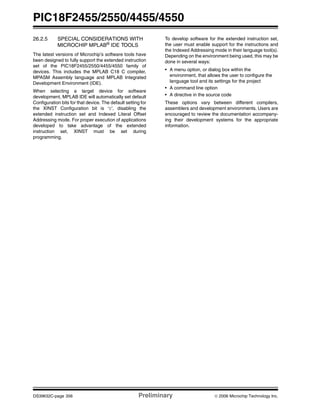
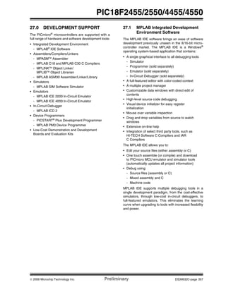
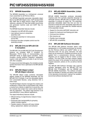
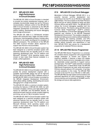
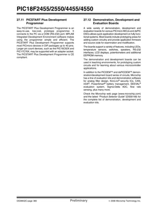
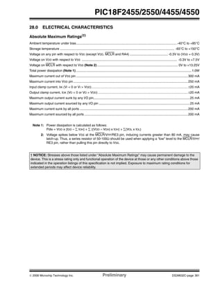
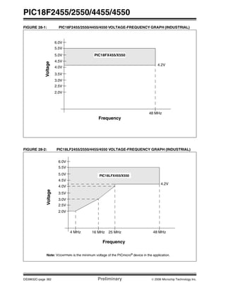
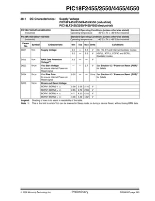
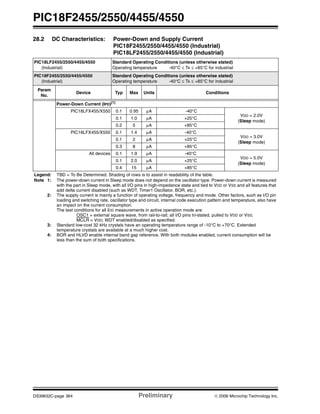
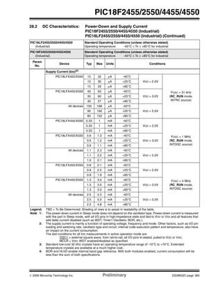
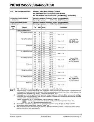
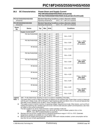
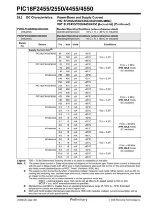
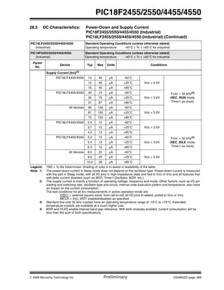
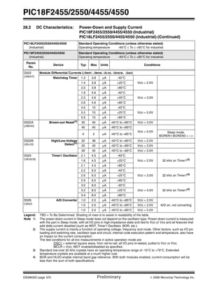
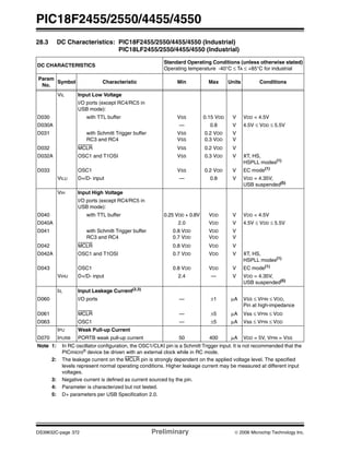
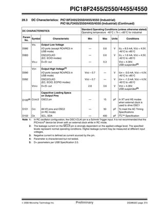
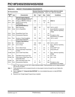
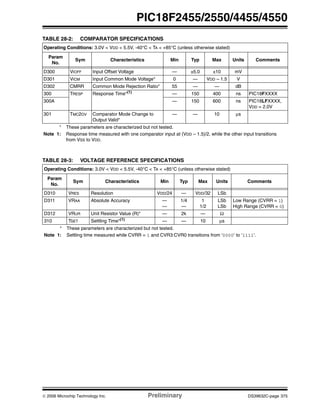
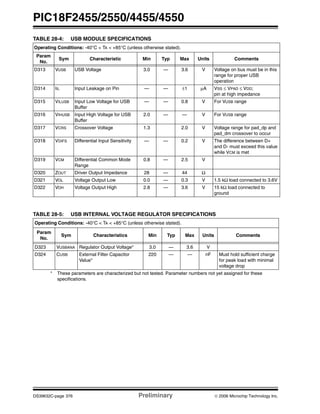
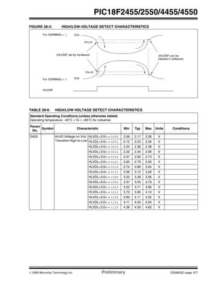
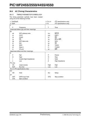
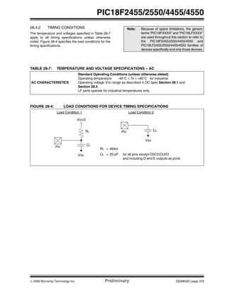
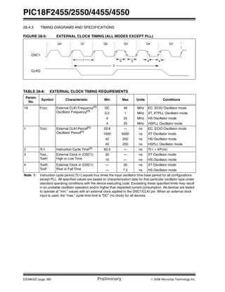
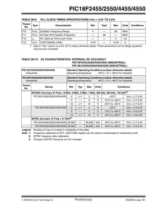
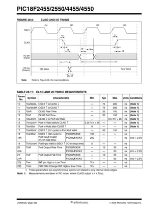
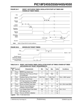
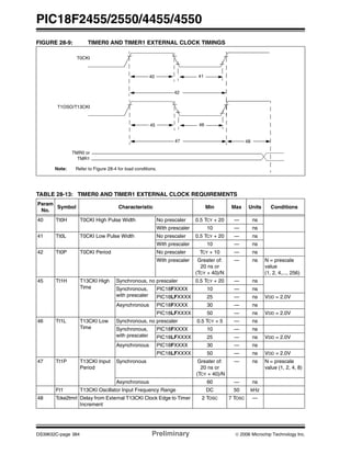
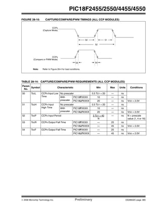
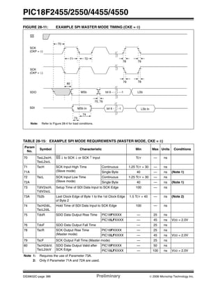
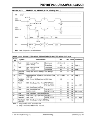
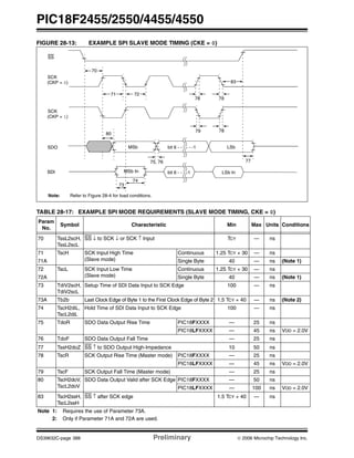
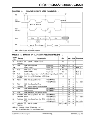
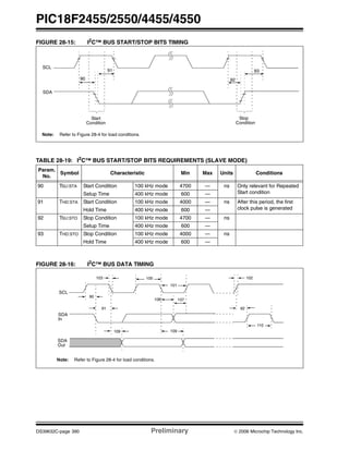
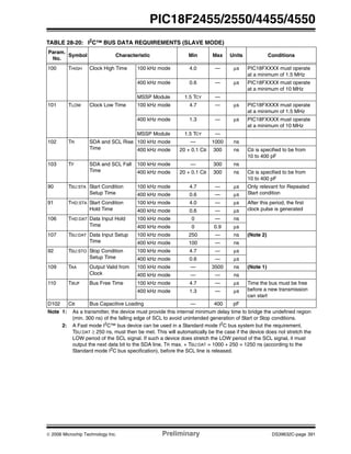
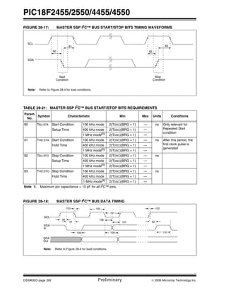
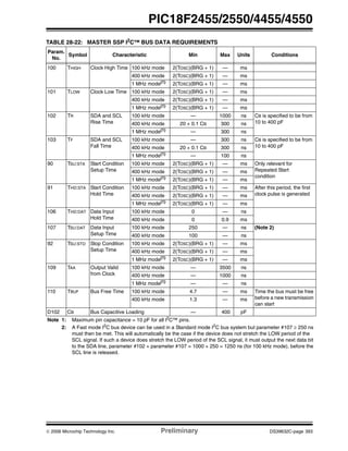
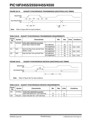
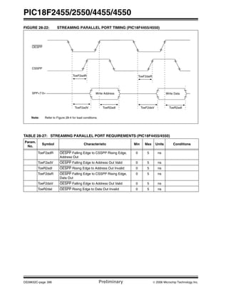
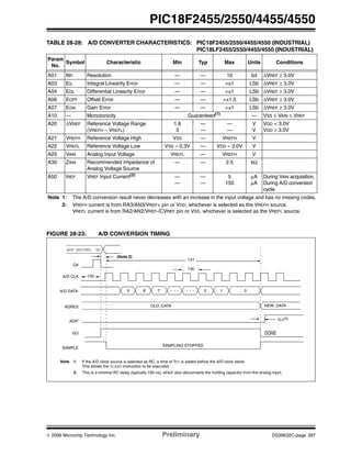
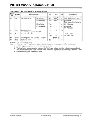


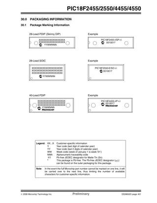

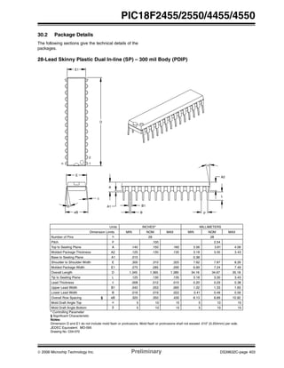
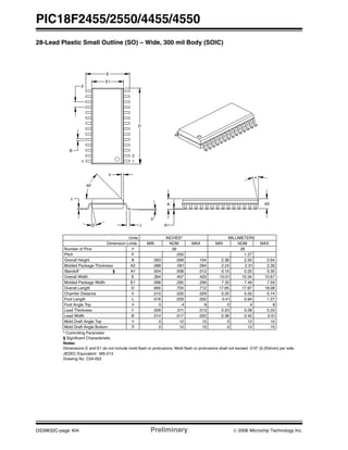
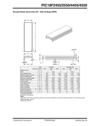
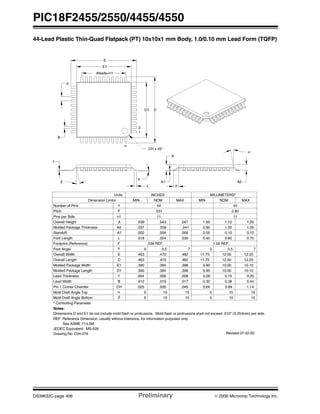


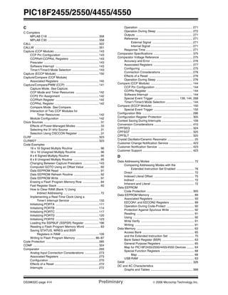
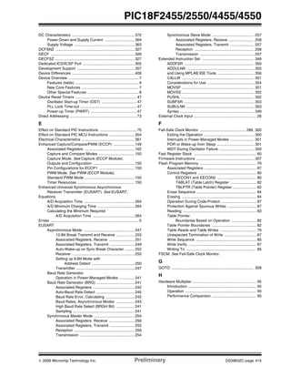
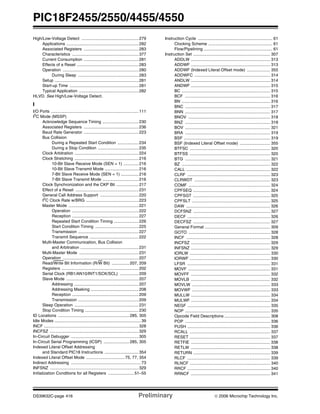
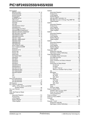
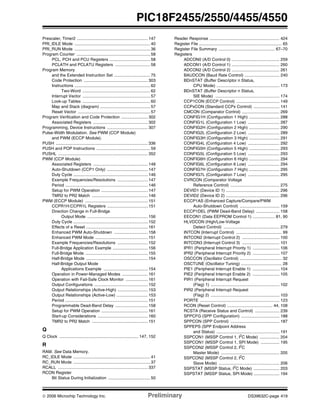
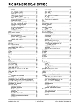
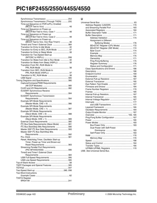
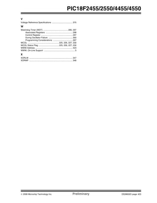

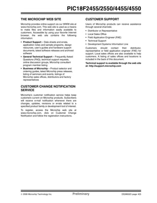


The document summarizes key features of Microchip's PIC18F2455/2550/4455/4550 microcontrollers including: - USB 2.0 support with on-chip transceiver and RAM - Low power modes down to 0.1uA typical - Flexible oscillator options including internal and external clocks - Peripherals such as timers, PWM, ADC, USART, I2C, and SPI - Flash program memory from 24K to 32K bytes and SRAM from 2048 to 4096 bytes