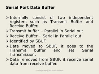
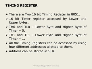
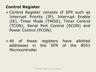
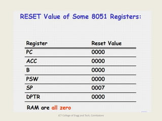
3. ACCUMULATOR
Its an operand Register.
It is referred as implicit or specified in the instruction
by its SFR address 0E0H.
Commonly used for Data Transfer and Arithmetic
Instructions.
It’s a bit addressable register.
Result stored in accumulator.
B REGISTER
Used in Multiplication and Division operations, to store
the second operand
Example: MUL AB, DIV AB
Upper 8 bits of multiplication and remainder incase if
division operation stored in B Register.
Also used as Temporary register, accessed by SFR
address 0F0H. It is a bit addressableJCT College of Engg and Tech, Coimbatore
7. STACK POINTER
8 – Bit Register
SP incremented before the data is stored onto
the stack using PUSH/CALL instruction
During PUSH , First increment SP and the copy
the data.
In a POP operation , initially copy data and then
decrement SP.
8 – bit address of the stack top is stored in this
register.
Stack located anywhere in the on chip 128 byte
RAM.
JCT College of Engg and Tech, Coimbatore
8. DATA POINTER
It is a 16 bit register.
Consist of Higher byte and Lower byte (DPH,DPL)
of a 16 bit external data RAM address.
Accessed by two 8 bit register or a 16 bit register.
DPTR has been given two address in the SFR.
Specially used for String operations and lookup
table operations.
With 16 bit DPTR, a maximum of 64K of off chip
data memory and a maximum of 64K of off chip
program memory can be addressed.
For this a 16 bit memory location address will be
stored in DPTR through MOV DPTR,#XXXX
JCT College of Engg and Tech, Coimbatore
9. PORT 0, 1, 2, 3 LATCHES AND DRIVERS
Each latch and corresponding driver of Ports 0 –
3 is allotted to the corresponding on chip I/O
port.
All the Ports are Bi – directional I/O ports of 8
bits each..
The addresses of Ports are stored in SFR.
Port 0 – I/O Lines and Multiplexed Address
(Lower Order) Data Lines.
Port 1 – Only I/O Lines
Port 2 - I/O Lines and Higher order Address
Lines
Port 3 – I/O Lines and Alternate functions
JCT College of Engg and Tech, Coimbatore
10. Serial Port Data Buffer
Internally consist of two independent
registers such as Transmit Buffer and
Receive Buffer.
Transmit buffer – Parallel in Serial out
Receive Buffer – Serial in Parallel out
Identified by SBUF.
Data moved to SBUF, it goes to the
Transmit buffer and set Serial
Transmission.
Data removed from SBUF, it receive serial
data from receive buffer.
JCT College of Engg and Tech, Coimbatore
11. TIMING REGISTER
There are Two 16 bit Timing Register in 8051.
16 bit Timer register accessed by Lower and
Upper bytes.
TH0 and TL0 – Lower Byte and Higher Byte of
Timer – 0.
TH1 and TL1 - Lower Byte and Higher Byte of
Timer – 1.
All the Timing Registers can be accessed by using
four different addresses allotted to them.
Address can be stored in SFR
JCT College of Engg and Tech, Coimbatore
12. Control Register
Control Register consists of SFR such as
Interrupt Priority (IP), Interrupt Enable
(IE), Timer Mode (TMOD), Timer Control
(TCON), Serial Port Control (SCON) and
Power Control (PCON).
All of these registers have allotted
addresses in the SFR of the 8051
Microcontroller
JCT College of Engg and Tech, Coimbatore