History Class XII Ch. 3 Kinship, Caste and Class (1).pptx
timing_diagram_of_8085.pptx
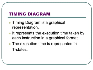
1. TIMING DIAGRAM
Timing Diagram is a graphical
representation.
It represents the execution time taken by
each instruction in a graphical format.
The execution time is represented in
T-states.
4. MACHINE CYCLE
The time required to access the memory
or input/output devices is called machine
cycle.
5. T-STATE
The machine cycle and instruction cycle
takes multiple clock periods.
A portion of an operation carried out in
one system clock period is called as T-
state.
6. MACHINE CYCLES OF 8085
The 8085 microprocessor has 5 basic machine
cycles.
They are
1. Opcode fetch cycle (4T)
2. Memory read cycle (3 T)
3. Memory write cycle (3 T)
4. I/O read cycle (3 T)
5. I/O write cycle (3 T)
7. MACHINE CYCLES OF 8085
The processor takes a definite time to
execute the machine cycles. The time
taken by the processor to execute a
machine cycle is expressed in T-states.
One T-state is equal to the time period of
the internal clock signal of the processor.
The T-state starts at the falling edge of a
clock.
8. OPCODE FETCH MACHINE
CYCLE OF 8085
Each instruction of the processor has one byte opcode.
The opcodes are stored in memory. So, the processor
executes the opcode fetch machine cycle to fetch the
opcode from memory.
Hence, every instruction starts with opcode fetch machine
cycle.
The time taken by the processor to execute the opcode
fetch cycle is 4T.
In this time, the first, 3 T-states are used for fetching the
opcode from memory and the remaining T-states are
used for internal operations by the processor.
10. MEMORY READ MACHINE
CYCLE OF 8085
The memory read machine cycle is executed
by the processor to read a data byte from
memory.
The processor takes 3T states to execute this
cycle
The instructions which have more than one
byte word size will use the machine cycle after
the opcode fetch machine cycle.
12. MEMORY WRITE MACHINE
CYCLE OF 8085
The memory write machine cycle is
executed by the processor to write a
data byte in a memory location.
The processor takes, 3T states to
execute this machine cycle
14. I/O READ CYCLE OF 8085
The I/O Read cycle is executed by the
processor to read a data byte from I/O
port or from the peripheral.
The processor takes 3T states to
execute this machine cycle.
The IN instruction uses this machine
cycle during the execution.
17. I/O WRITE CYCLE OF 8085
The I/O write machine cycle is executed
by the processor to write a data byte in
the I/O port or to a peripheral, which is
I/O, mapped in the system.
The processor takes, 3T states to
execute this machine cycle.
18. Timing diagram
Problem – Draw the timing diagram of
the given instruction in 8085
MOV B, C
Given instruction copy the contents of
the source register into the destination
register and the contents of the source
register are not altered.
19. Timing diagram
MOV B, C
Opcode: MOV
Operand: B and C
Here the destination register and C is the
source register whose contents need to be
transferred to the destination register.
Algorithm – The instruction MOV B, C is of 1
byte; therefore the complete instruction will
be stored in a single memory address
20. Timing diagram
2000: MOV B, C
Only opcode fetching is required for this
instruction and thus we need 4 T states
for the timing diagram. For the opcode
fetch the IO/M (low active) = 0, S1 = 1
and S0 = 1
22. Explanation of diagram
00 – lower bit of address where the opcode is stored, i.e., 00.
20 – higher bit of address where the opcode is stored, i.e., 20.
ALE – provides signal for multiplexed address and data bus. Only in t1
is it used as an address bus to fetch a lower bit of address otherwise it
will be used as the data bus.
RD (low active) – signal is 1 in t1 & t4 as no data is read by the
microprocessor. Signal is 0 in t2 & t3 because here the data is read by
a microprocessor.
WR (low active) – signal is 1 throughout, no data is written by a
microprocessor.
IO/M (low active) – signal is 1 throughout because the operation is
performing on memory.
S0 and S1 – both are 1 in case of opcode fetching.
23. Draw the timing diagram of the following
code,
MVI B, 43
24. Explanation of the command
It stores the immediate 8 bit data to a
register or memory location.
Example: MVI B, 43
Opcode: MVI
Operand: B is the destination register and 43
is the source data which needs to be
transferred to the register.
’43’ data will be stored in the B register.
25. Explanation of the command
Assume the memory address of the opcode and the data. For
example:
MVI B, 43
2000: Opcode
2001: 43
The opcode fetch will be same in all the instructions.
Only the read instruction of the opcode needs to be added in
the successive T states.
For the opcode fetch the IO/M (low active) = 0, S1 = 1 and S0 =
1. Also, 4 T states will be required to fetch the opcode from
memory.
For the opcode read the IO/M (low active) = 0, S1 = 1 and S0 =
0. Also, only 3 T states will be required to read data from
memory.
27. In Opcode fetch ( t1-t4 T states )
00 – lower bit of address where opcode is stored.
20 – higher bit of address where opcode is stored.
ALE – Provides signal for multiplexed address and data bus. Only in t1
it used as address bus to fetch lower bit of address otherwise it will be
used as data bus.
RD (low active) – Signal is 1 in t1 & t4, no data is read by
microprocessor. Signal is 0 in t2 & t3, data is read by microprocessor.
WR (low active) – Signal is 1 throughout, no data is written by
microprocessor.
IO/M (low active) – Signal is 0 in throughout, operation is performing
on memory.
S0 and S1 – Signal is 1 in t1 to t4 states, as to fetch the opcode from
the memory.
28. In Opcode read ( t5-t7 T states )
01 – lower bit of address where data is stored.
20 – higher bit of address where data is stored.
ALE – Provides signal for multiplexed address and data bus. Only in t5 it used
as address bus to fetch lower bit of address otherwise it will be used as data
bus.
RD (low active) – Signal is 1 in t5 as no data is read by microprocessor. Signal
is 0 in t6 & t7 as data is read by microprocessor.
WR (low active) – Signal is 1 throughout, no data is written by microprocessor.
IO/M (low active) – Signal is 0 in throughout, operation is performing on
memory.
S0 – Signal is 0 in throughout, operation is performing on memory to read data
43.
S1 – Signal is 1 throughout, operation is performing on memory to read data
43.
30. Timing Diagram for STA 526AH
STA means Store Accumulator -The content of the accumulator is
stored in the specified address (526A). this instruction SDA 4050H
requires 3-Bytes, 4-Machine Cycles (Opcode Fetch, Memory Read,
Memory Read, Memory Write) and 13 T-States for execution
The op-code of the STA instruction is said to be 32H. It is fetched from
the memory 41FFH (see fig). - OF machine cycle
Then the lower order memory address is read (6A). – Memory Read
Machine Cycle
Read the higher order memory address (52).- Memory Read Machine
Cycle
The combination of both the addresses is considered and the content
from accumulator is written in 526A. – Memory Write Machine Cycle
Assume the memory address for the instruction and let the content of
accumulator is C7H. So, C7H from accumulator is now stored in 526A
31. Explanation of the command
Address Memories Hex-code
41FFH STA 32H
4200H 6AH 6AH
4201H 52H 52H
526AH C7H C7H
33. OUT a8 instruction in 8085
Microprocessor
OUT is a mnemonic that stands for
OUTput Accumulator contents to an
output port whose8-bit address is
indicated in the instruction . It occupies 2
Bytes in the memory. First Byte specifies
the opcode, and the next Byte provides
the 8-bit port address.
34. Explanation of the command
Mnemonics, Operand Opcode(in HEX) Bytes
OUT Port-Address D3 2
35. Explanation of the command
OUT instruction is the only instruction using
which Accumulator contents can be sent out
to an output port. A possible chip select
circuit to connect an output port with an
address as F0H.
So this instruction OUT requires 2-Bytes, 3-
Machine Cycles (Opcode Fetch, Memory
Read, I/O write) and 10 T-States
36. Explanation of the command
Addr
ess
Hex
Code
s
Mnemo
nic
Comment
200
0
D3 OUT
F0H
Accumulator content will be sent to
port addressF0H
201 F0 F0H as port address