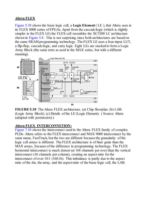
SlideShare a Scribd company logo
1 of 10
Altera FLEX
Figure 5.10 shows the basic logic cell, a Logic Element ( LE ), that Altera uses in
its FLEX 8000 series of FPGAs. Apart from the cascadelogic (which is slightly
simpler in the FLEX LE) the FLEX cell resembles the XC5200 LC architecture
shown in Figure 5.8 . This is not surprising since both architectures are based on
the same SRAM programming technology. The FLEX LE uses a four-input LUT,
a flip-flop, cascadelogic, and carry logic. Eight LEs are stacked to form a Logic
Array Block (the same term as used in the MAX series, but with a different
meaning).
FIGURE 5.10 The Altera FLEX architecture. (a) Chip floorplan. (b) LAB
(Logic Array Block). (c) Details of the LE (Logic Element). ( Source: Altera
(adapted with permission).)
Altera FLEX INTERCONNETION:
Figure 7.10 shows the interconnect used in the Altera FLEX family of complex
PLDs. Altera refers to the FLEX interconnect and MAX 9000 interconnect by the
same name, FastTrack, but the two are different because the granularity of the
logic cell arrays is different. The FLEX architecture is of finer grain than the
MAX arrays_because of the difference in programming technology. The FLEX
horizontal interconnect is much denser (at 168 channels per row) than the vertical
interconnect (16 channels per column), creating an aspectratio for the
interconnect of over 10:1 (168:16). This imbalance is partly due to the aspect
ratio of the die, the array, and the aspectratio of the basic logic cell, the LAB.
FIGURE 7.10 The Altera FLEX interconnect scheme. (a) The row and column
FastTrackinterconnect. The chip shown, with 4 rows ¥ 21 columns, is the same
size as the EPF8820. (b) A simplified diagram of the interconnect architecture
showing the connections between the FastTrack buses and a LAB. Boxes A, B,
and C represent the bus-to-bus connections.
As an example, the EPF8820 has 4 rows and 21 columns of LABs ( Figure 7.10
a). Ignoring, for simplicity’s sake, what happens at the edge of the die we can
total the routing channels as follows:
 Horizontal channels = 4 rows x 168 channels/row = 672 channels.
 Vertical channels = 21 rows x 16 channels/row = 336 channels.
It appears that there is still approximately twice (672:336) as much interconnect
capacity in the horizontal direction as the vertical. If we look inside the boxes A,
B, and C in Figure 7.10 (b) we see that for individual lines on each bus:
 Box A connects an LE to two row channels.
 Box B connects two column channels to a row channel.
 Box C connects an LE to two column channels.
There is some dependence between boxes A and B since they contain MUXes
rather than direct connections, but essentially there are twice as many
connections to the column FastTrack as the row FastTrack, thus restoring the
balance in interconnect capacity.
Altera FLEX 8000 Block Diagram:
The FLEX 8000 device family is ideal for a variety of applications because it combines
the fine-grained architecture and high register count characteristics of FPGAs with the
high speed and predictable interconnect delays of EPLDs. Logic is implemented in
LEs that include compact4-input look-up tables (LUTs) and programmable registers.
FLEX 8000 chip contains 26–162 LABs.
● Each LAB contains 8 Logic Elements (LEs), so a chip contains 208–1296 LEs,
totaling 2,500–16,000 usable gates.
● LABs arranged in rows and columns, connected by FastTrackInterconnect, with I/O
elements (IOEs) at the edges.
`
 LAB = 8 LEs, plus local interconnect,control signals, carry & cascade
chains.
Altera FLEX 8000 Logic Array Block:
Altera FLEX 8000 Logic Element:
Each Logic Element (LE) contains:
● 4-input Look-Up Table (LUT)
Can produceany function of 4 variables
● Programmable flip-flop
Can configure as D, T, JR, SR, or bypass
Has clock, clear, and preset signals that can come from dedicated
inputs, I/O pins, or other LEs
● Carrychain provides very fast (< 1ns)
carry-forward between LEs
● Feeds both LUT and next part of chain
● Good forhigh-speed adders & counters
 Cascade chain provides wide fan-in.
● Adjacent LE’s LUTs can compute parts of the function in parallel;
cascadechain then serially connects intermediate values.
● Can use either a logical AND or a logical OR (using DeMorgan’s
theorem) to connectoutputs of adjacent LEs.
● Each additional LE provides 4 more inputs to the width of the function
Altera FLEX 8000 Configuration:
Loading the FLEX 8000’s SRAM with programming information is
called configuration, and takes about 100ms
● After configuration, the device initializes itself (resets its registers,
enables its I/O pins, and begins normal operation)
● Configuration & initialization = command mode, normal operation =
user mode
Six configuration schemes are available:
● Active serial — FLEX gives configuration EPROM clock signals (not
addresses), keeps getting new values in sequence
● Active parallel up, active parallel down — FLEX 8000 gives
configuration EPROMsequence of addresses to read data from some
host.
● Passive parallel synchronous, passiveparallel asynchronous, passive
serial — passively receives data from some host.
Altera FLEX 8000 LE Operating Modes
Normal mode
● Used for general logic applications, and wide decoding functions that
can benefit from the cascade chain.
Arithmetic mode
● Provides two 3-input LUTs to implement adders, accumulators, and
comparators.
One LUT provides a 3-bit function.
Other LUT generates a carry bit.
7 Fall 2004, Lecture21
Up/down counter mode
● Provides counter enable, synchronous up / down control, and data
loading options.
● Uses two 3-input LUTs
One LUT generates counter data.
Other LUT generates fast carry bit.
Use 2-to-1 multiplexer for synchronous data loading, clear and preset
for asynchronousdata loading.
Altera FLEX 10K Block Diagram:
FLEX 10K chip contains 72–1520 LABs
● Each LAB contains 8 Logic Elements (LEs), so a chip contains 576–12,160
LEs, totaling 10,000–250,000 usable gates.
Each chip also contains 3–20 Embedded Array Blocks (EABs),
which can provide 6,164–40,960 bits of RAM.
Altera FLEX 10K Embedded Array Blocks (EABs):
Each chip contains 3–20 EABs, each of which can be used to implement either
logic or memory.
When used to implement logic, an EAB can provide 100 to 600 gate
equivalents (in contrast, a LAB provides 96 g.e.’s)
● Provides a very large LUT.
Very fast — faster than general logic, since it’s only a
single level of logic.
Delay is predictable — each RAM block is not scattered
throughout the chip as in some FPGAs.
● Can be used to create complex logic functions such as multipliers (e.g.,
a 4x4 multiplier with 8 inputs and 8 outputs), microcontrollers, large
state machines, and DSPs.
● Each EAB can be used independently, or combined to implement larger
functions.
Using EABs to implement memory, a chip can have 6K–40K bits of
RAM.
● Each EAB provides 2,048 bits of RAM, plus input and output
registers.
● Can be used to implement synchronous RAM, ROM, dual-port
RAM, or FIFO.
● Each EAB can be configured in the following sizes:
256x8, 512x4, 1024x2, or 2048x1
● To get larger blocks, combine multiple EABs:
Example: combine two 256x8 RAM blocks to form a
256x16 RAM block.
Can combine so as to form blocks up to 2048 words without
impacting timing and EAB gets input from a row channel, and can
output to up to 2 row channels and 2 column channels.
Input and output buffers are available.
Altera FLEX 10K Embedded Array Blocks :

More Related Content

What's hot

Introduction to Embedded System I: Chapter 2 (5th portion)
Introduction to Embedded System I: Chapter 2 (5th portion)Introduction to Embedded System I: Chapter 2 (5th portion)
Introduction to Embedded System I: Chapter 2 (5th portion)Moe Moe Myint
 
Fpga(field programmable gate array)
Fpga(field programmable gate array) Fpga(field programmable gate array)
Fpga(field programmable gate array) Iffat Anjum
 
Seminar on field programmable gate array
Seminar on field programmable gate arraySeminar on field programmable gate array
Seminar on field programmable gate arraySaransh Choudhary
 
System On Chip
System On ChipSystem On Chip
System On Chipanishgoel
 
Level sensitive scan design(LSSD) and Boundry scan(BS)
Level sensitive scan design(LSSD) and Boundry scan(BS)Level sensitive scan design(LSSD) and Boundry scan(BS)
Level sensitive scan design(LSSD) and Boundry scan(BS)Praveen Kumar
 
VLSI Testing Techniques
VLSI Testing TechniquesVLSI Testing Techniques
VLSI Testing TechniquesA B Shinde
 
Complex Programmable Logic Device (CPLD) Architecture and Its Applications
Complex Programmable Logic Device (CPLD) Architecture and Its ApplicationsComplex Programmable Logic Device (CPLD) Architecture and Its Applications
Complex Programmable Logic Device (CPLD) Architecture and Its Applicationselprocus
 
Overview of digital design with Verilog HDL
Overview of digital design with Verilog HDLOverview of digital design with Verilog HDL
Overview of digital design with Verilog HDLanand hd
 
Hardware Software Codesign
Hardware Software CodesignHardware Software Codesign
Hardware Software Codesigndestruck
 
vlsi design flow
vlsi design flowvlsi design flow
vlsi design flowAnish Gupta
 
Design and development of carry select adder
Design and development of carry select adderDesign and development of carry select adder
Design and development of carry select adderABIN THOMAS
 
ASIC DESIGN : PLACEMENT
ASIC DESIGN : PLACEMENTASIC DESIGN : PLACEMENT
ASIC DESIGN : PLACEMENThelloactiva
 
VLSI subsystem design processes and illustration
VLSI subsystem design processes and illustrationVLSI subsystem design processes and illustration
VLSI subsystem design processes and illustrationVishal kakade
 

What's hot (20)

Introduction to Embedded System I: Chapter 2 (5th portion)
Introduction to Embedded System I: Chapter 2 (5th portion)Introduction to Embedded System I: Chapter 2 (5th portion)
Introduction to Embedded System I: Chapter 2 (5th portion)
 
SRAM
SRAMSRAM
SRAM
 
Fpga(field programmable gate array)
Fpga(field programmable gate array) Fpga(field programmable gate array)
Fpga(field programmable gate array)
 
FPGA
FPGAFPGA
FPGA
 
Seminar on field programmable gate array
Seminar on field programmable gate arraySeminar on field programmable gate array
Seminar on field programmable gate array
 
System On Chip
System On ChipSystem On Chip
System On Chip
 
Level sensitive scan design(LSSD) and Boundry scan(BS)
Level sensitive scan design(LSSD) and Boundry scan(BS)Level sensitive scan design(LSSD) and Boundry scan(BS)
Level sensitive scan design(LSSD) and Boundry scan(BS)
 
Fpga
FpgaFpga
Fpga
 
VLSI Testing Techniques
VLSI Testing TechniquesVLSI Testing Techniques
VLSI Testing Techniques
 
ARM CORTEX M3 PPT
ARM CORTEX M3 PPTARM CORTEX M3 PPT
ARM CORTEX M3 PPT
 
Complex Programmable Logic Device (CPLD) Architecture and Its Applications
Complex Programmable Logic Device (CPLD) Architecture and Its ApplicationsComplex Programmable Logic Device (CPLD) Architecture and Its Applications
Complex Programmable Logic Device (CPLD) Architecture and Its Applications
 
Introduction to FPGAs
Introduction to FPGAsIntroduction to FPGAs
Introduction to FPGAs
 
Overview of digital design with Verilog HDL
Overview of digital design with Verilog HDLOverview of digital design with Verilog HDL
Overview of digital design with Verilog HDL
 
Hardware Software Codesign
Hardware Software CodesignHardware Software Codesign
Hardware Software Codesign
 
vlsi design flow
vlsi design flowvlsi design flow
vlsi design flow
 
Design and development of carry select adder
Design and development of carry select adderDesign and development of carry select adder
Design and development of carry select adder
 
Unit 3 mpmc
Unit 3 mpmcUnit 3 mpmc
Unit 3 mpmc
 
ASIC DESIGN : PLACEMENT
ASIC DESIGN : PLACEMENTASIC DESIGN : PLACEMENT
ASIC DESIGN : PLACEMENT
 
Vlsi stick daigram (JCE)
Vlsi stick daigram (JCE)Vlsi stick daigram (JCE)
Vlsi stick daigram (JCE)
 
VLSI subsystem design processes and illustration
VLSI subsystem design processes and illustrationVLSI subsystem design processes and illustration
VLSI subsystem design processes and illustration
 

Similar to Altera flex

Microprocessor questions converted
Microprocessor questions convertedMicroprocessor questions converted
Microprocessor questions convertedArghodeepPaul
 
Specialist officer it study material on organization of intel 8085 microproce...
Specialist officer it study material on organization of intel 8085 microproce...Specialist officer it study material on organization of intel 8085 microproce...
Specialist officer it study material on organization of intel 8085 microproce...Tamal Kumar Das
 
5 unit.pdf vlsi unit 2 important notes for ece department
5 unit.pdf vlsi unit 2 important notes for ece department5 unit.pdf vlsi unit 2 important notes for ece department
5 unit.pdf vlsi unit 2 important notes for ece departmentnitcse
 
System designing and modelling using fpga
System designing and modelling using fpgaSystem designing and modelling using fpga
System designing and modelling using fpgaIAEME Publication
 
Spartan-II FPGA (xc2s30)
Spartan-II FPGA (xc2s30)Spartan-II FPGA (xc2s30)
Spartan-II FPGA (xc2s30)A B Shinde
 
Microprocessor and Microcontroller.pdf
Microprocessor and Microcontroller.pdfMicroprocessor and Microcontroller.pdf
Microprocessor and Microcontroller.pdfLatif Khan
 
EEE- BEE603 - Microprocessor and Microcontroller- Mr K Dwarakesh_220819_18121...
EEE- BEE603 - Microprocessor and Microcontroller- Mr K Dwarakesh_220819_18121...EEE- BEE603 - Microprocessor and Microcontroller- Mr K Dwarakesh_220819_18121...
EEE- BEE603 - Microprocessor and Microcontroller- Mr K Dwarakesh_220819_18121...NaWinNK
 
VLSI design Dr B.jagadeesh UNIT-5.pptx
VLSI design Dr B.jagadeesh   UNIT-5.pptxVLSI design Dr B.jagadeesh   UNIT-5.pptx
VLSI design Dr B.jagadeesh UNIT-5.pptxjagadeesh276791
 
etherlink plus developers guide
etherlink plus developers guideetherlink plus developers guide
etherlink plus developers guidepanamjayait
 
8051 final word
8051 final word8051 final word
8051 final wordhandson28
 
Microprocessor 8085
Microprocessor 8085Microprocessor 8085
Microprocessor 8085Dhaval Barot
 
Ece 8085-microprocessor-ppt
Ece 8085-microprocessor-pptEce 8085-microprocessor-ppt
Ece 8085-microprocessor-pptsatyamshra
 
INTEL 8086 MICROPROCESSOR
INTEL 8086 MICROPROCESSORINTEL 8086 MICROPROCESSOR
INTEL 8086 MICROPROCESSORSagar Kuntumal
 

Similar to Altera flex (20)

Microprocessor questions converted
Microprocessor questions convertedMicroprocessor questions converted
Microprocessor questions converted
 
Specialist officer it study material on organization of intel 8085 microproce...
Specialist officer it study material on organization of intel 8085 microproce...Specialist officer it study material on organization of intel 8085 microproce...
Specialist officer it study material on organization of intel 8085 microproce...
 
5 unit.pdf vlsi unit 2 important notes for ece department
5 unit.pdf vlsi unit 2 important notes for ece department5 unit.pdf vlsi unit 2 important notes for ece department
5 unit.pdf vlsi unit 2 important notes for ece department
 
System designing and modelling using fpga
System designing and modelling using fpgaSystem designing and modelling using fpga
System designing and modelling using fpga
 
4_BIT_ALU
4_BIT_ALU4_BIT_ALU
4_BIT_ALU
 
Intermediate Fabrics
Intermediate FabricsIntermediate Fabrics
Intermediate Fabrics
 
Fpga 03-cpld-and-fpga
Fpga 03-cpld-and-fpgaFpga 03-cpld-and-fpga
Fpga 03-cpld-and-fpga
 
Spartan-II FPGA (xc2s30)
Spartan-II FPGA (xc2s30)Spartan-II FPGA (xc2s30)
Spartan-II FPGA (xc2s30)
 
Eec503, mp 30 questions
Eec503, mp 30 questionsEec503, mp 30 questions
Eec503, mp 30 questions
 
Eec503, mp 30 questions
Eec503, mp 30 questionsEec503, mp 30 questions
Eec503, mp 30 questions
 
Microprocessor and Microcontroller.pdf
Microprocessor and Microcontroller.pdfMicroprocessor and Microcontroller.pdf
Microprocessor and Microcontroller.pdf
 
EEE- BEE603 - Microprocessor and Microcontroller- Mr K Dwarakesh_220819_18121...
EEE- BEE603 - Microprocessor and Microcontroller- Mr K Dwarakesh_220819_18121...EEE- BEE603 - Microprocessor and Microcontroller- Mr K Dwarakesh_220819_18121...
EEE- BEE603 - Microprocessor and Microcontroller- Mr K Dwarakesh_220819_18121...
 
VLSI design Dr B.jagadeesh UNIT-5.pptx
VLSI design Dr B.jagadeesh   UNIT-5.pptxVLSI design Dr B.jagadeesh   UNIT-5.pptx
VLSI design Dr B.jagadeesh UNIT-5.pptx
 
8086 microprocessor
8086 microprocessor8086 microprocessor
8086 microprocessor
 
etherlink plus developers guide
etherlink plus developers guideetherlink plus developers guide
etherlink plus developers guide
 
8051 final word
8051 final word8051 final word
8051 final word
 
Microprocessor 8085
Microprocessor 8085Microprocessor 8085
Microprocessor 8085
 
8086
80868086
8086
 
Ece 8085-microprocessor-ppt
Ece 8085-microprocessor-pptEce 8085-microprocessor-ppt
Ece 8085-microprocessor-ppt
 
INTEL 8086 MICROPROCESSOR
INTEL 8086 MICROPROCESSORINTEL 8086 MICROPROCESSOR
INTEL 8086 MICROPROCESSOR
 

Recently uploaded

Gfe Mayur Vihar Call Girls Service WhatsApp -> 9999965857 Available 24x7 ^ De...
Gfe Mayur Vihar Call Girls Service WhatsApp -> 9999965857 Available 24x7 ^ De...Gfe Mayur Vihar Call Girls Service WhatsApp -> 9999965857 Available 24x7 ^ De...
Gfe Mayur Vihar Call Girls Service WhatsApp -> 9999965857 Available 24x7 ^ De...srsj9000
 
Internship report on mechanical engineering
Internship report on mechanical engineeringInternship report on mechanical engineering
Internship report on mechanical engineeringmalavadedarshan25
 
HARMONY IN THE NATURE AND EXISTENCE - Unit-IV
HARMONY IN THE NATURE AND EXISTENCE - Unit-IVHARMONY IN THE NATURE AND EXISTENCE - Unit-IV
HARMONY IN THE NATURE AND EXISTENCE - Unit-IVRajaP95
 
main PPT.pptx of girls hostel security using rfid
main PPT.pptx of girls hostel security using rfidmain PPT.pptx of girls hostel security using rfid
main PPT.pptx of girls hostel security using rfidNikhilNagaraju
 
College Call Girls Nashik Nehal 7001305949 Independent Escort Service Nashik
College Call Girls Nashik Nehal 7001305949 Independent Escort Service NashikCollege Call Girls Nashik Nehal 7001305949 Independent Escort Service Nashik
College Call Girls Nashik Nehal 7001305949 Independent Escort Service NashikCall Girls in Nagpur High Profile
 
Oxy acetylene welding presentation note.
Oxy acetylene welding presentation note.Oxy acetylene welding presentation note.
Oxy acetylene welding presentation note.eptoze12
 
Call Girls Delhi {Jodhpur} 9711199012 high profile service
Call Girls Delhi {Jodhpur} 9711199012 high profile serviceCall Girls Delhi {Jodhpur} 9711199012 high profile service
Call Girls Delhi {Jodhpur} 9711199012 high profile servicerehmti665
 
(ANVI) Koregaon Park Call Girls Just Call 7001035870 [ Cash on Delivery ] Pun...
(ANVI) Koregaon Park Call Girls Just Call 7001035870 [ Cash on Delivery ] Pun...(ANVI) Koregaon Park Call Girls Just Call 7001035870 [ Cash on Delivery ] Pun...
(ANVI) Koregaon Park Call Girls Just Call 7001035870 [ Cash on Delivery ] Pun...ranjana rawat
 
Sheet Pile Wall Design and Construction: A Practical Guide for Civil Engineer...
Sheet Pile Wall Design and Construction: A Practical Guide for Civil Engineer...Sheet Pile Wall Design and Construction: A Practical Guide for Civil Engineer...
Sheet Pile Wall Design and Construction: A Practical Guide for Civil Engineer...Dr.Costas Sachpazis
 
Heart Disease Prediction using machine learning.pptx
Heart Disease Prediction using machine learning.pptxHeart Disease Prediction using machine learning.pptx
Heart Disease Prediction using machine learning.pptxPoojaBan
 
HARMONY IN THE HUMAN BEING - Unit-II UHV-2
HARMONY IN THE HUMAN BEING - Unit-II UHV-2HARMONY IN THE HUMAN BEING - Unit-II UHV-2
HARMONY IN THE HUMAN BEING - Unit-II UHV-2RajaP95
 
High Profile Call Girls Nagpur Meera Call 7001035870 Meet With Nagpur Escorts
High Profile Call Girls Nagpur Meera Call 7001035870 Meet With Nagpur EscortsHigh Profile Call Girls Nagpur Meera Call 7001035870 Meet With Nagpur Escorts
High Profile Call Girls Nagpur Meera Call 7001035870 Meet With Nagpur EscortsCall Girls in Nagpur High Profile
 
SPICE PARK APR2024 ( 6,793 SPICE Models )
SPICE PARK APR2024 ( 6,793 SPICE Models )SPICE PARK APR2024 ( 6,793 SPICE Models )
SPICE PARK APR2024 ( 6,793 SPICE Models )Tsuyoshi Horigome
 
Architect Hassan Khalil Portfolio for 2024
Architect Hassan Khalil Portfolio for 2024Architect Hassan Khalil Portfolio for 2024
Architect Hassan Khalil Portfolio for 2024hassan khalil
 
High Profile Call Girls Nagpur Isha Call 7001035870 Meet With Nagpur Escorts
High Profile Call Girls Nagpur Isha Call 7001035870 Meet With Nagpur EscortsHigh Profile Call Girls Nagpur Isha Call 7001035870 Meet With Nagpur Escorts
High Profile Call Girls Nagpur Isha Call 7001035870 Meet With Nagpur Escortsranjana rawat
 
VIP Call Girls Service Kondapur Hyderabad Call +91-8250192130
VIP Call Girls Service Kondapur Hyderabad Call +91-8250192130VIP Call Girls Service Kondapur Hyderabad Call +91-8250192130
VIP Call Girls Service Kondapur Hyderabad Call +91-8250192130Suhani Kapoor
 
VICTOR MAESTRE RAMIREZ - Planetary Defender on NASA's Double Asteroid Redirec...
VICTOR MAESTRE RAMIREZ - Planetary Defender on NASA's Double Asteroid Redirec...VICTOR MAESTRE RAMIREZ - Planetary Defender on NASA's Double Asteroid Redirec...
VICTOR MAESTRE RAMIREZ - Planetary Defender on NASA's Double Asteroid Redirec...VICTOR MAESTRE RAMIREZ
 
APPLICATIONS-AC/DC DRIVES-OPERATING CHARACTERISTICS
APPLICATIONS-AC/DC DRIVES-OPERATING CHARACTERISTICSAPPLICATIONS-AC/DC DRIVES-OPERATING CHARACTERISTICS
APPLICATIONS-AC/DC DRIVES-OPERATING CHARACTERISTICSKurinjimalarL3
 

Recently uploaded (20)

Gfe Mayur Vihar Call Girls Service WhatsApp -> 9999965857 Available 24x7 ^ De...
Gfe Mayur Vihar Call Girls Service WhatsApp -> 9999965857 Available 24x7 ^ De...Gfe Mayur Vihar Call Girls Service WhatsApp -> 9999965857 Available 24x7 ^ De...
Gfe Mayur Vihar Call Girls Service WhatsApp -> 9999965857 Available 24x7 ^ De...
 
Internship report on mechanical engineering
Internship report on mechanical engineeringInternship report on mechanical engineering
Internship report on mechanical engineering
 
HARMONY IN THE NATURE AND EXISTENCE - Unit-IV
HARMONY IN THE NATURE AND EXISTENCE - Unit-IVHARMONY IN THE NATURE AND EXISTENCE - Unit-IV
HARMONY IN THE NATURE AND EXISTENCE - Unit-IV
 
main PPT.pptx of girls hostel security using rfid
main PPT.pptx of girls hostel security using rfidmain PPT.pptx of girls hostel security using rfid
main PPT.pptx of girls hostel security using rfid
 
🔝9953056974🔝!!-YOUNG call girls in Rajendra Nagar Escort rvice Shot 2000 nigh...
🔝9953056974🔝!!-YOUNG call girls in Rajendra Nagar Escort rvice Shot 2000 nigh...🔝9953056974🔝!!-YOUNG call girls in Rajendra Nagar Escort rvice Shot 2000 nigh...
🔝9953056974🔝!!-YOUNG call girls in Rajendra Nagar Escort rvice Shot 2000 nigh...
 
College Call Girls Nashik Nehal 7001305949 Independent Escort Service Nashik
College Call Girls Nashik Nehal 7001305949 Independent Escort Service NashikCollege Call Girls Nashik Nehal 7001305949 Independent Escort Service Nashik
College Call Girls Nashik Nehal 7001305949 Independent Escort Service Nashik
 
Oxy acetylene welding presentation note.
Oxy acetylene welding presentation note.Oxy acetylene welding presentation note.
Oxy acetylene welding presentation note.
 
Exploring_Network_Security_with_JA3_by_Rakesh Seal.pptx
Exploring_Network_Security_with_JA3_by_Rakesh Seal.pptxExploring_Network_Security_with_JA3_by_Rakesh Seal.pptx
Exploring_Network_Security_with_JA3_by_Rakesh Seal.pptx
 
Call Girls Delhi {Jodhpur} 9711199012 high profile service
Call Girls Delhi {Jodhpur} 9711199012 high profile serviceCall Girls Delhi {Jodhpur} 9711199012 high profile service
Call Girls Delhi {Jodhpur} 9711199012 high profile service
 
(ANVI) Koregaon Park Call Girls Just Call 7001035870 [ Cash on Delivery ] Pun...
(ANVI) Koregaon Park Call Girls Just Call 7001035870 [ Cash on Delivery ] Pun...(ANVI) Koregaon Park Call Girls Just Call 7001035870 [ Cash on Delivery ] Pun...
(ANVI) Koregaon Park Call Girls Just Call 7001035870 [ Cash on Delivery ] Pun...
 
Sheet Pile Wall Design and Construction: A Practical Guide for Civil Engineer...
Sheet Pile Wall Design and Construction: A Practical Guide for Civil Engineer...Sheet Pile Wall Design and Construction: A Practical Guide for Civil Engineer...
Sheet Pile Wall Design and Construction: A Practical Guide for Civil Engineer...
 
Heart Disease Prediction using machine learning.pptx
Heart Disease Prediction using machine learning.pptxHeart Disease Prediction using machine learning.pptx
Heart Disease Prediction using machine learning.pptx
 
HARMONY IN THE HUMAN BEING - Unit-II UHV-2
HARMONY IN THE HUMAN BEING - Unit-II UHV-2HARMONY IN THE HUMAN BEING - Unit-II UHV-2
HARMONY IN THE HUMAN BEING - Unit-II UHV-2
 
High Profile Call Girls Nagpur Meera Call 7001035870 Meet With Nagpur Escorts
High Profile Call Girls Nagpur Meera Call 7001035870 Meet With Nagpur EscortsHigh Profile Call Girls Nagpur Meera Call 7001035870 Meet With Nagpur Escorts
High Profile Call Girls Nagpur Meera Call 7001035870 Meet With Nagpur Escorts
 
SPICE PARK APR2024 ( 6,793 SPICE Models )
SPICE PARK APR2024 ( 6,793 SPICE Models )SPICE PARK APR2024 ( 6,793 SPICE Models )
SPICE PARK APR2024 ( 6,793 SPICE Models )
 
Architect Hassan Khalil Portfolio for 2024
Architect Hassan Khalil Portfolio for 2024Architect Hassan Khalil Portfolio for 2024
Architect Hassan Khalil Portfolio for 2024
 
High Profile Call Girls Nagpur Isha Call 7001035870 Meet With Nagpur Escorts
High Profile Call Girls Nagpur Isha Call 7001035870 Meet With Nagpur EscortsHigh Profile Call Girls Nagpur Isha Call 7001035870 Meet With Nagpur Escorts
High Profile Call Girls Nagpur Isha Call 7001035870 Meet With Nagpur Escorts
 
VIP Call Girls Service Kondapur Hyderabad Call +91-8250192130
VIP Call Girls Service Kondapur Hyderabad Call +91-8250192130VIP Call Girls Service Kondapur Hyderabad Call +91-8250192130
VIP Call Girls Service Kondapur Hyderabad Call +91-8250192130
 
VICTOR MAESTRE RAMIREZ - Planetary Defender on NASA's Double Asteroid Redirec...
VICTOR MAESTRE RAMIREZ - Planetary Defender on NASA's Double Asteroid Redirec...VICTOR MAESTRE RAMIREZ - Planetary Defender on NASA's Double Asteroid Redirec...
VICTOR MAESTRE RAMIREZ - Planetary Defender on NASA's Double Asteroid Redirec...
 
APPLICATIONS-AC/DC DRIVES-OPERATING CHARACTERISTICS
APPLICATIONS-AC/DC DRIVES-OPERATING CHARACTERISTICSAPPLICATIONS-AC/DC DRIVES-OPERATING CHARACTERISTICS
APPLICATIONS-AC/DC DRIVES-OPERATING CHARACTERISTICS
 

Altera flex

  • 1. Altera FLEX Figure 5.10 shows the basic logic cell, a Logic Element ( LE ), that Altera uses in its FLEX 8000 series of FPGAs. Apart from the cascadelogic (which is slightly simpler in the FLEX LE) the FLEX cell resembles the XC5200 LC architecture shown in Figure 5.8 . This is not surprising since both architectures are based on the same SRAM programming technology. The FLEX LE uses a four-input LUT, a flip-flop, cascadelogic, and carry logic. Eight LEs are stacked to form a Logic Array Block (the same term as used in the MAX series, but with a different meaning). FIGURE 5.10 The Altera FLEX architecture. (a) Chip floorplan. (b) LAB (Logic Array Block). (c) Details of the LE (Logic Element). ( Source: Altera (adapted with permission).) Altera FLEX INTERCONNETION: Figure 7.10 shows the interconnect used in the Altera FLEX family of complex PLDs. Altera refers to the FLEX interconnect and MAX 9000 interconnect by the same name, FastTrack, but the two are different because the granularity of the logic cell arrays is different. The FLEX architecture is of finer grain than the MAX arrays_because of the difference in programming technology. The FLEX horizontal interconnect is much denser (at 168 channels per row) than the vertical interconnect (16 channels per column), creating an aspectratio for the interconnect of over 10:1 (168:16). This imbalance is partly due to the aspect ratio of the die, the array, and the aspectratio of the basic logic cell, the LAB.
  • 2. FIGURE 7.10 The Altera FLEX interconnect scheme. (a) The row and column FastTrackinterconnect. The chip shown, with 4 rows ¥ 21 columns, is the same size as the EPF8820. (b) A simplified diagram of the interconnect architecture showing the connections between the FastTrack buses and a LAB. Boxes A, B, and C represent the bus-to-bus connections. As an example, the EPF8820 has 4 rows and 21 columns of LABs ( Figure 7.10 a). Ignoring, for simplicity’s sake, what happens at the edge of the die we can total the routing channels as follows:  Horizontal channels = 4 rows x 168 channels/row = 672 channels.  Vertical channels = 21 rows x 16 channels/row = 336 channels. It appears that there is still approximately twice (672:336) as much interconnect capacity in the horizontal direction as the vertical. If we look inside the boxes A, B, and C in Figure 7.10 (b) we see that for individual lines on each bus:  Box A connects an LE to two row channels.  Box B connects two column channels to a row channel.  Box C connects an LE to two column channels. There is some dependence between boxes A and B since they contain MUXes rather than direct connections, but essentially there are twice as many connections to the column FastTrack as the row FastTrack, thus restoring the balance in interconnect capacity. Altera FLEX 8000 Block Diagram: The FLEX 8000 device family is ideal for a variety of applications because it combines the fine-grained architecture and high register count characteristics of FPGAs with the high speed and predictable interconnect delays of EPLDs. Logic is implemented in LEs that include compact4-input look-up tables (LUTs) and programmable registers. FLEX 8000 chip contains 26–162 LABs. ● Each LAB contains 8 Logic Elements (LEs), so a chip contains 208–1296 LEs, totaling 2,500–16,000 usable gates.
  • 3. ● LABs arranged in rows and columns, connected by FastTrackInterconnect, with I/O elements (IOEs) at the edges. `  LAB = 8 LEs, plus local interconnect,control signals, carry & cascade chains.
  • 4. Altera FLEX 8000 Logic Array Block:
  • 5. Altera FLEX 8000 Logic Element: Each Logic Element (LE) contains: ● 4-input Look-Up Table (LUT) Can produceany function of 4 variables ● Programmable flip-flop Can configure as D, T, JR, SR, or bypass Has clock, clear, and preset signals that can come from dedicated inputs, I/O pins, or other LEs ● Carrychain provides very fast (< 1ns) carry-forward between LEs ● Feeds both LUT and next part of chain ● Good forhigh-speed adders & counters  Cascade chain provides wide fan-in. ● Adjacent LE’s LUTs can compute parts of the function in parallel; cascadechain then serially connects intermediate values.
  • 6. ● Can use either a logical AND or a logical OR (using DeMorgan’s theorem) to connectoutputs of adjacent LEs. ● Each additional LE provides 4 more inputs to the width of the function Altera FLEX 8000 Configuration: Loading the FLEX 8000’s SRAM with programming information is called configuration, and takes about 100ms ● After configuration, the device initializes itself (resets its registers, enables its I/O pins, and begins normal operation) ● Configuration & initialization = command mode, normal operation = user mode Six configuration schemes are available: ● Active serial — FLEX gives configuration EPROM clock signals (not addresses), keeps getting new values in sequence ● Active parallel up, active parallel down — FLEX 8000 gives configuration EPROMsequence of addresses to read data from some host. ● Passive parallel synchronous, passiveparallel asynchronous, passive serial — passively receives data from some host. Altera FLEX 8000 LE Operating Modes Normal mode ● Used for general logic applications, and wide decoding functions that can benefit from the cascade chain. Arithmetic mode ● Provides two 3-input LUTs to implement adders, accumulators, and comparators. One LUT provides a 3-bit function. Other LUT generates a carry bit.
  • 7. 7 Fall 2004, Lecture21 Up/down counter mode ● Provides counter enable, synchronous up / down control, and data loading options. ● Uses two 3-input LUTs One LUT generates counter data. Other LUT generates fast carry bit. Use 2-to-1 multiplexer for synchronous data loading, clear and preset for asynchronousdata loading.
  • 8. Altera FLEX 10K Block Diagram: FLEX 10K chip contains 72–1520 LABs ● Each LAB contains 8 Logic Elements (LEs), so a chip contains 576–12,160 LEs, totaling 10,000–250,000 usable gates. Each chip also contains 3–20 Embedded Array Blocks (EABs), which can provide 6,164–40,960 bits of RAM. Altera FLEX 10K Embedded Array Blocks (EABs): Each chip contains 3–20 EABs, each of which can be used to implement either logic or memory. When used to implement logic, an EAB can provide 100 to 600 gate equivalents (in contrast, a LAB provides 96 g.e.’s) ● Provides a very large LUT. Very fast — faster than general logic, since it’s only a single level of logic. Delay is predictable — each RAM block is not scattered throughout the chip as in some FPGAs.
  • 9. ● Can be used to create complex logic functions such as multipliers (e.g., a 4x4 multiplier with 8 inputs and 8 outputs), microcontrollers, large state machines, and DSPs. ● Each EAB can be used independently, or combined to implement larger functions. Using EABs to implement memory, a chip can have 6K–40K bits of RAM. ● Each EAB provides 2,048 bits of RAM, plus input and output registers. ● Can be used to implement synchronous RAM, ROM, dual-port RAM, or FIFO. ● Each EAB can be configured in the following sizes: 256x8, 512x4, 1024x2, or 2048x1 ● To get larger blocks, combine multiple EABs: Example: combine two 256x8 RAM blocks to form a 256x16 RAM block. Can combine so as to form blocks up to 2048 words without impacting timing and EAB gets input from a row channel, and can output to up to 2 row channels and 2 column channels. Input and output buffers are available.
  • 10. Altera FLEX 10K Embedded Array Blocks :