Recommended

Recommended
More Related Content
What's hot
What's hot (19)
Viewers also liked
Viewers also liked (16)
Similar to Design 3.4GHz High Power Amplifier for Ranging Transponder
Similar to Design 3.4GHz High Power Amplifier for Ranging Transponder (20)
Design 3.4GHz High Power Amplifier for Ranging Transponder
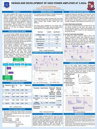
- 1. DESIGN AND DEVELOPMENT OF HIGH POWER AMPLIFIER AT 3.4GHz Neel Patel (140320705506) Guided by: Asst. Prof. Nimesh M Prabhakar L.J. Institute of Engineering and Technology INTRODUCTION OF IRNSS MATCHING NETWORK DESIGN REFERENCES HARMONIC BALANCE IN ADS • Due to this output signal contains fundamental frequency components and some undesired frequency components, which are integral multiple of input signal frequency. These additional frequency components are called harmonics. Hence the output is said to be distorted, this is called harmonic distortion. 1st Order Harmonic f1=3GHz f2=4GHz 3rd Order Harmonic 2f1-f2=2GHz 2f2-f1=5GHz 5th Order harmonic 3f1-2f2=100 MHz 3f2-2f1=6GHz CONCLUTION • In a communication satellite serving the earth, the transponder transforms the received signals into forms appropriate for the transmission from space to earth. The transponder may be simply a repeater that amplifies and frequency signals. In this paper, the technologies of the major transponder elements are presented and amplifying devices. • The transmitter is required to amplify the wanted signal without distortions and without other impairments which would decrease the usefulness of the signal. Two types of amplifiers (transmitters) are in common use, electron beam devices (commonly TWTAs) and solid state power amplifiers (SSPAs). For the TWTAs, the electrical power supply is often required to supply a number of high voltages , which presents a series of technology and design challenges. show in fig 1. The Power Amplifier presented here does meet many of the required specifications. The transistor is Stable for design specifications.The choice of transistor in this power amplifier has influenced the design specifications in an unexpected manner. To make a power amplifier utilizing this device, a wide variety of matching networks should be explored along with an appropriate device modelling in ADS. Also Complete the Impedance Matching , Biasing Network , Harmonics Balance. RANGING TRANSPONDER MASTER CONTROL STATION DIPLEXER RECEIVER BPF TRANSMITER (PA) ANTENNA CDMA 6.7 GHz 3.4 GHz Fig 1: Indian Regional Navigational Satellite System DESIGN APPROACH • The wireless communications in satellite transponder increasing demands on systems designs. • A critical element in Radio Frequency (RF) front ends is the Power Amplifier (PA). Main specifications for PA design include high linearity, better gain and efficiency. • The active device specified for this design was a Rfmd SZA3044Z BJT. Table I shows the performance specifications for the designed Power amplifier.. Parameter Symbol Specification Frequency range fo 2.5-4.5 GHz Gain S21 ≥15dB Input return loss S11 ≤ -10dB Output return loss S22 ≤ -10dB Input/output Impedance Z0 50Ω Output power P0 1W Table 2 : Target Specification • Impedance matching is required to maximize the power transfer and minimize the reflections. Smith chart is used for impedance matching. According to maximum power transfer theorem, maximum power delivered to the load when the impedance of load is equal to the complex conjugate of the impedance of source (ZS=ZL*). A. INPUT MATCHING NETWORK • The first set of measurements we are taken for S11 with the device mounted on the board and biased, but without matching networks. These measurements were de-embedded in ADS to obtain the input impedance at the device terminal. B. OUTPUT MATCHING NETWORK • To design the output matching network, S22 of the biased, unmatched system was measured and de- embedded back to the device terminals. Simulations were then performed to determine the impedance presented to the drain that would maximize small signal gain. The matching network was designed in the same fashion as the input matching network. Fig 2: Input & Output Matching Network Circuit In ADS DC I/V CHARACTRISTICS • We have to define the Output Power and Power Efficiency of the Amplifier with the help of the DC IV Characteristics. • The Biasing condition Vce = 5V , Idc = 240 mA • Result: RF Output Power: 1.33W DC Power Output: 2.47W Efficiency= 𝑅𝐹𝑂𝑢𝑡𝑝𝑢𝑡 𝑃𝑜𝑤𝑒𝑟 𝐷𝐶 𝑜𝑢𝑡𝑝𝑢𝑡 𝑃𝑜𝑤𝑒𝑟 ∗ 100% = 1.33𝑊 2.47𝑊 *100% =54% Fig 5: Stability Factor Fig 6 : Harmonic balance Fig 9 : Harmonic Balance Fig 7 : OrdersFig 8 : 1st & 3rd Order Output RESULTS Parameter Specification Measured results After Impedance Matching Measure d results After Biasing Network Gain S21 ≥15dB 26.412dB 27.064dB Input return loss S11 ≤ -10dB -39.873dB - 15.440dB Output return loss S22 ≤ -10dB -49.342dB - 15.725dB Input/output Impedance Z0 50Ω 50Ω 50Ω Table 3 : Measurement Results BIASING NETWORK OF POWER AMPLIFIER Fig 4 : Gain Of Power Amplifier Fig 3 : After Biasing Network Of Power Amplifier Fig 5: Stability Factor • The power amplifier (PA), being one of the most important blocks of the wireless communication system, is no exception. Therefore, this document presents a detailed study of the single-ended class- A power amplifier, which is the configuration that has good efficiency and easier integration, making it one of the strongest candidates for a practical implementation. The aim of this work is to provide the study that guides the design of a high power amplifier at 3.4 GHz for Ranging Transponder applications. ABSTRACT LITERATURE SURVEY Rf No Frequency Gain (S21) S11 S22 Efficiency 1 3.5GHz 33dB -10dB -10dB 30% 2 0.2 – 8GHz 13.2d B -9.1dB -12dB 39% 3 3.4GHz 14dB -10dB -10dB 25% 4 3.5GHz 16dB -30dB -31dB 45% 5 5.8GHz 9dB -19dB -19dB 50% Table 1 : Literature Survey 1. Tomohiro Senju, Takashi Asano, Hiroshi Ishimura Microwave Solid-state Department “A VERY SMALL 3.5 GHz 1 W MMIC POWER AMPLIFIER WITH DIE SIZE REDUCTION TECHNOLOGIES” Komukai Operations Toshiba Corporation, Toshiba-cho, Saiwai-ku, Kawasaki 2 12-858 1, Japan-2001 IEEE, pp. 070-073 ,ISBN:0-7803-7161-5/01. 2. Kevin W. Kobayashi, YaoChung Chen, Ioulia Smorchkova, Roger Tsai,Mike Wojtowicz, and Aaron Oki “A 2 Watt, Sub-dB Noise Figure GaN MMIC LNA-PA Amplifier with Multi- octave Bandwidth from 0.2-8 GHz” 2007 IEEE - SIRENZA MICRODEVICES, pp.619 - 622,ISBN:1-4244-0688-9/07. 3. Paul saad, christian fager, hossein mashad nemati, haiying cao, herbert zirath and kristoffer andersson ” A highly efficient 3.5 GHz inverse class-F GaN HEMT power amplifier” European Microwave Association International Journal of Microwave and Wireless Technologies, 2010, 2(3-4), pp.317–332,DOI:10.1017.