This document provides information about a Digital Electronics and Logic Design (DELD) course. It includes:
- The course name, code, semester, credits, and faculty member.
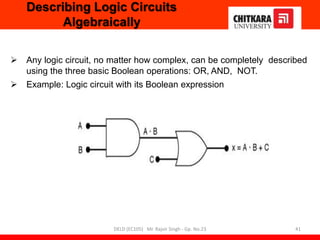
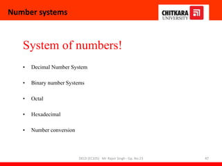
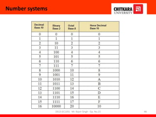
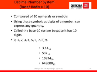
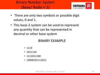
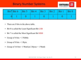
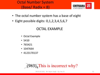
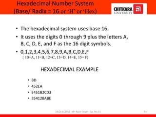
- An overview of the course content which teaches fundamentals of digital logic design, number systems, logic elements, circuit design and optimization.
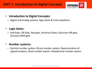
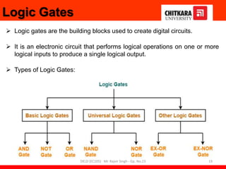
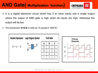
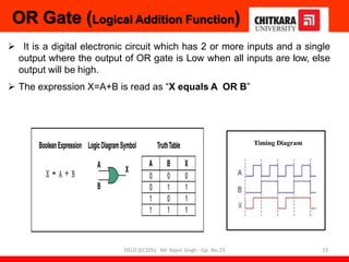
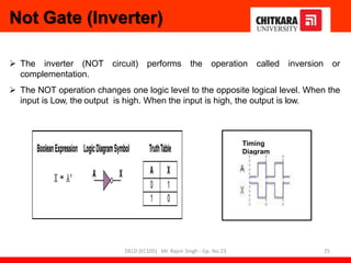
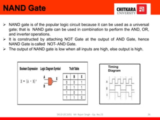
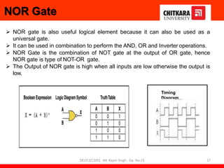
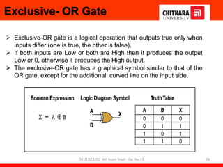
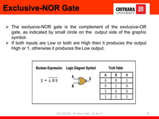
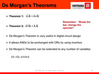
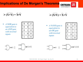
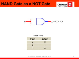
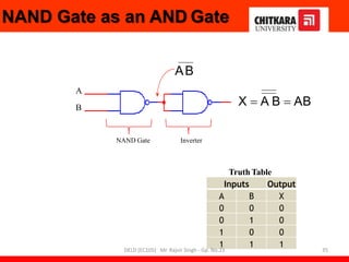
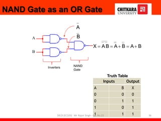
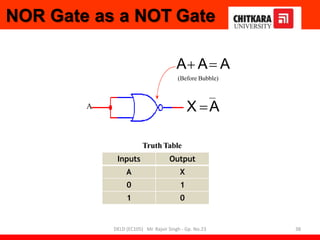
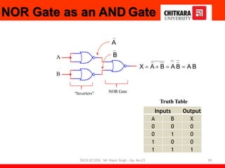
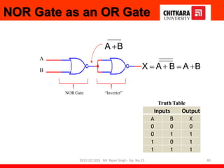
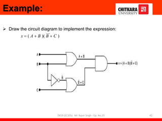
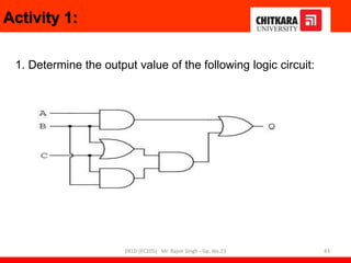
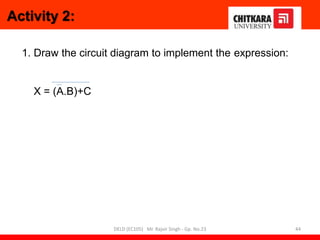
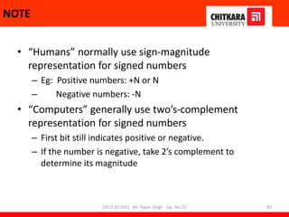
- Descriptions of logic gates like AND, OR, NOT, NAND and NOR gates along with their truth tables and diagrams.
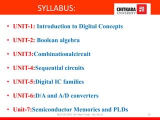
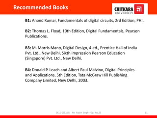
- Details about the syllabus, course outcomes, recommended books and the content of the first unit on digital concepts and logic gates.