
Recommended
Recommended
More Related Content
What's hot
What's hot (20)
Similar to Microstrip Transmission line On HFSS , all reports S parameters , impedance , electric vector field
Similar to Microstrip Transmission line On HFSS , all reports S parameters , impedance , electric vector field (20)
Recently uploaded
Recently uploaded (20)
Microstrip Transmission line On HFSS , all reports S parameters , impedance , electric vector field
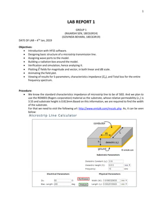
- 1. 1 LAB REPORT 1 GROUP 1 (RAJARSHI SEN, 18EC63R14) (GOVINDA BEHARA, 18EC63R19) DATE OF LAB – 4TH Jan, 2019 Objectives: • Introduction with HFSS software. • Designing basic structure of a microstrip transmission line. • Assigning wave ports to the model. • Building a radiation box around the model. • Verification and simulation, hence analyzing it. • Plotting 𝐸⃗ fields for magnitude and vector, in both linear and dB scale. • Animating the field plot. • Viewing of results for S-parameters, characteristics impedance (𝑍0), and Total loss for the entire frequency spectrum. Procedure: • We know the standard characteristics impedance of microstrip line to be of 50Ω. And we plan to use the RO4003 (Rogers corporation) material as the substrate, whose relative permeability (𝜖 𝑟) is 3.55 and substrate height is 0.813mm.Based on this information, we are required to find the width of the substrate. For that we need to visit the following url: http://www.emtalk.com/mscalc.php. As, it can be seen below:
- 2. 2 • There, all the values are put up. Frequency was taken as 10GHz, and the electrical length is of not much importance, as its contribution to the width calculation is minimal. Then we get the synthesized value of the width to be 1.81865mm. The second synthesized parameter, the Length is again of less importance to us, so we ignored it. • To start our design, we are needed to open up the HFSS software, which looks like: • At first we designed the substrate, and for that we are needed to plot an arbitrary 3d box . The reference grid is XY plane. To design the 3d box, two approaches can be taken: o Drawing through the shortcut button: If we look carefully at the top, we will see a 3d box icon which looks like: Clicking it, will let us draw the 3d box. o Alternatively, we can take up the original procedure of going through Draw > box. It can be seen below:
- 3. 3 • Once we do that, then we get the markings on the grid that assists in drawing up the 3d box: • Once, we are satisfied with the arbitrary box, we finalized it and the selected structure built up: • Next, we are required to change the box dimensions, so that we can make it up as the substrate and it was suggested that we keep the origin of the space at the center of the bottom of the substrate. We assumed the dimensions of the substrate to be the variables a,b and h such that a=20mm, b=40mm and h=0.813mm(h was known earlier as the property of RO4003c material). Variables assignment is deemed advantageous over direct values, as it gives the flexibility to change the model dimensions without changing the physical structure altogether. The box that we created was arbitrarily named box1 and we can see it in the left side tab:
- 4. 4 • Then the following operations are performed: Right click on “CreateBox” > Properties • In HFSS, while defining the position, we need to refer to the starting position. So, for our model of the substrate of dimension (a,b,h), the starting position would be (-a/2,-b/2 and 0) and the size would be X axis – a, Y axis – b and Z axis – h. These valued have to be entered at the following pop up window. It can be seen below:
- 5. 5 Following the variables declaration and position assignment, there opens successive popup for variables definition, as seen above. • Following that, we could see the final substrate dimension shaped up: • Next, we changed the property of the substrate from vacuum to RO4003C and also changed the name of the material for convenience. The procedure for it is: Right click on “Box1” > Properties
- 6. 6 • In the popup window, we changed the name, and from the materials tab, we get the edit options, where we searched for the desired material (RO4003C). The color of the substrate was also changed to brown.
- 7. 7 • The ground plane is of same dimension as that of the substrate in x and y axis. The only difference arises in the material type (copper) and thickness. So, the substrate was selected and copied (selecting the substrate then ctrl + c and ctrl +v). A new material under RO4003C named substrate1 was made. • Following procedure is undertaken: Right click on substrate 1 > Properties • The material was edited from the tab and copper was selected. Also name was changed and the color was changed to saffron. • Then to change the physical location of the ground plane: Right click on CreateBox > properties
- 8. 8 • The starting location of the ground plane is same as that of the substrate (-a/2,-b/2,0), and the size of the ground plane a,b,-t. the thickness t is taken as negative (-t) because the thickness of the ground plane will exist from Z=0 to z= -t. The thickness of the ground sheet was selected as 17𝜇𝑚 (0.017mm). • Then we visually verified the formation of ground plane below the substrate.
- 9. 9 • Next task was designing the microstrip. As its width was different from that of the substrate and ground sheet, it was simpler to design the microstrip from beginning. For that we created an arbitrary 3d box as before and then edited the physical dimension. The starting location of the microstrip was –w/2,-b/2,h and the region was –w/2<X<w/2, -b/2<Y<b/2 and h<Z<h+t. Then the size was X = w, Y = b and z = t. It was observed that the t is taken positive as the z region starts from h and grows upward toward h+t. The width was earlier calculated to be 1.81865mm.
- 10. 10 • The name of the microstrip was changed from Box1 to “microstrip”, material changed to copper and color changed to saffron. • The finalized model was visible:
- 11. 11 • Next task was assigning of wave ports. For that we first changed the grid reference plane from XY to XZ plane. First we searched for an icon resembling the following figure: Then we get the dropdown menu and we select the desired plane. • The change of grid plane was visible • The ports are drawn as rectangular figures. For this again two approaches could have been followed: o Searching for the rectangular figure icon and selecting it. It looked like below: o Draw > Rectangle • Its physical starting dimensions are -3*w,-b/2,-t. It is known that the optimized value of the wave port is six times the width of microstrip and 6 times the height of the substrate. It is defined as below:
- 12. 12 • This was copied to form the next wave port and physical starting location was altered by changing starting y location from –b/2 to b/2: • The wave ports are visualized. • Next we assigned wave port to the rectangular box that was just drawn. For that: Right click on Rectangle1 > Assign Excitation > Wave port
- 13. 13 • Name was kept as 1:
- 14. 14 • Then an integration line was drawn: • While drawing the line, we would get triangle symbols when cursor is at the exact center: • If the previous procedure was done correctly, then it would show that the line was defined:
- 15. 15 • We can see that one of the sheets are classified as wave port: • Then, similarly we will define the other sheet as wave port. After that, we can see that both the sheets are under the category of wave port.
- 16. 16 • The next task was to verify the excitation of the wave port. For that, under the project manager tab, we need to click on the excitation and then the respective port. • Then we can see some regular geometry over the wave port, confirming the excitation
- 17. 17 • Next we were tasked with the design of a radiation box cover the microstrip transmission line. For that, again, arbitrarily a 3d box was designed and, its material was selected as vacuum and given the name of Rad_Box, also, color was set to light blue and transparency value was set to 0.9, allowing us to see the contents inside the radiation box. • Then the physical dimensions were to be set. Generally the dimensions are such that, the radiation box exceeds the substrate by the length of 𝜆0/4. In our case, it was a simple model, so for convenience, we took the radiation box dimension as (a+20mm,b,h+20mm), and the starting position was ((-a/2)-10mm,-b/2,0mm-10mm).
- 18. 18 • We could visualize the radiation box, and also the contents inside due to the assigned transparency. • Then, we have to assign the property of the radiation boundary to the radiation box. For that Right click on Rad_Box > Assign Boundary > Radiation
- 19. 19 • The name was left as Rad1 • Then, to check for the boundary assignment we can click on the boundary option on the left hand pane and then select Rad1.
- 20. 20 • Then we can view the regular geometry over the radiation box and be satisfied with the boundary application. • The radiation box was made invisible. For that, we open the active view visibility, and for that we look for the icon with eye shape as given below: Then, clicking it will open up the checkbox list for all the objects. We uncheck the Rad_Box.
- 21. 21 • The next step came for the simulation of the arrangement. For that we were needed to add a solution setup. Right click on Analysis > Add Solution Setup • In the following popup window, the solution setup was set to 10GHz, as it is an broadband structure, so center frequency was selected as the Solution Frequency (In narrowband structures, the upper frequency is generally set as the solution frequency). The numbers of passes (number of iterations) are selected as 20 (this parameter depends upon the processing capability of the device).
- 22. 22 • Then, we defined the frequency sweep Right click on Setup1 > Add Frequency Sweep • The sweep type was selected as Fast sweep. • Start frequency and stop frequency were taken up as 5GHz and 15GHz respectively. Step size was selected as 0.02.
- 23. 23 • Then we need to verify the validity of the model. For this we looked up for a green icon resembling a tick symbol as shown below. • Clicking it shows whether all is done properly or otherwise. • Once validation is verified, simulation had to begin. For this again another green icon next to the previous one, resembling exclamation sign was clicked, which looked like the following: • Following that, another popup opened up for saving the project and we named it as “Microstrip report”.
- 24. 24 • Then simulation began, and we understood by some red progressive bars in the bottom right corner • Once the simulation ends, we will get the notification and also the red bars will not be there. • We checked the fields on the wave port, by selecting Port field display, then 1 and then Port 1. • Then appeared the field view.
- 25. 25 • We were interested in the region consisting of the microstrip, so we zoomed over to it. The red arrows are strongest in the domain of magnitude. This result was reasonable. • Next we checked the S-parameters, for this we needed to open the rectangular plot window Right click on Results > Create Modal Solution Data Report > Rectangular Plot
- 26. 26 • From the following window, S Parameters were selected from the drop down menu. Both the S(1,1) and S(2,1) were selected and the scale selected was dB. • The S(2,1) should ideally be 1 in linear scale and 0 in dB, and S(1,1) should ideally be 0 in linear scale and -∞ dB (in practical scenario, it would be some large negative value). The results we obtained were:
- 27. 27 • We checked the magnitude of Electric field Right click on substrate > Plot fields > E > Mag_E • Frequency was selected as 10GHz and solution type was selected as sweep
- 28. 28 • To view the field, field overlays was selected, then E field and finally Mag_E1. • We could see the plot of the radiation fields within the substrate.
- 29. 29 • The fields were concentrated mostly on the center. To see it more clearly, it was desired to view this in log scale. For this we right clicked on the plot scale and selected the option “Modify”. • Then, in the following window, under the “scale” tab log was selected.
- 30. 30 • We could then see the fields more spread out, due to the log scale view. • Next we went for the Vector electric fields. Right click on substrate > Plot fields > E > Vector_E
- 31. 31 • Following the popup, again we selected the frequency to be 10Hz. • We could visualize the Vector Electric fields.
- 32. 32 • We then performed the animation of the radiation over the substrate. Right click on Mag_E1 > Animate • Swept variable was kept as “Phase” The animation was then visible.
- 33. 33 • As we went by the standard characteristics impedance of 50Ω, next we verified the port impedance. Right click on Results > Create Modal Solution Data Report > Rectangular Plot • In the following window under the port Zo category, both Zo(1) and Zo(2) were selected and scale was selected as Magnitude.
- 34. 34 • The characteristics impedance (𝑍0) for both the ports under entire frequency range was visible. • Then we checked the total loss through port 1. The following steps were taken: Right click on Results > Create Modal Solution Data Report > Rectangular Plot
- 35. 35 • As the total loss is not a predefined variable, so we were needed to define it. From the popup window, “output variables” is clicked upon. • We know the total loss for port1 can be given as: 𝑇𝑜𝑡𝑎𝑙 𝐿𝑜𝑠𝑠 = 1 − |𝑆(1,1)|2 − |𝑆(2,1)|2 This equation was then written upon the expression space and added • We had to confirm the addition of this new variable.
- 36. 36 • We followed through, selecting the new output variable we created • We could see the plot representing total loss for entire frequency range. Results: • We gained familiarity with HFSS software. • We successfully designed and tested the microstrip transmission line. • The objectives were fulfilled.