8051 microcontroller training (2) (sahil gupta 9068557926)
•Download as PPT, PDF•
2 likes•1,189 views

Training PPT on 8051 microcontroller

Recommended
Recommended
More Related Content
What's hot
What's hot (20)
Viewers also liked
Similar to 8051 microcontroller training (2) (sahil gupta 9068557926)
Similar to 8051 microcontroller training (2) (sahil gupta 9068557926) (20)
More from Sahil Gupta
More from Sahil Gupta (6)
Recently uploaded
Recently uploaded (20)
8051 microcontroller training (2) (sahil gupta 9068557926)
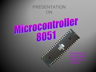
- 1. PRESENTATION ON Submitted by : RUPAL KAUL ECE Final yr 2110021
- 2. The microprocessor is the core of computer systems. Nowadays many communication, digital entertainment, portable devices, are controlled by them. A designer should know what types of components he needs, ways to reduce production costs and product reliable.
- 3. CPU: Central Processing Unit I/O: Input /Output Bus: Address bus & Data bus Memory: RAM & ROM Timer Interrupt Serial Port Parallel Port
- 4. CPU General- Purpose Micro- processor RAM ROM I/O Port Timer Serial COM Port Data Bus Address Bus General-Purpose Microprocessor System CPU for Computers No RAM, ROM, I/O on CPU chip itself Example : Intel’s x86, Motorola’s 680x0 Many chips on mother’s board General-purpose microprocessor
- 5. RAM ROM I/O Port Timer Serial COM Port Microcontroller CPU A smaller computer On-chip RAM, ROM, I/O ports... Example : Motorola’s 6811, Intel’s 8051, Zilog’s Z8 and PIC 16X A single chip Microcontroller :
- 6. Microprocessor CPU is stand-alone, RAM, ROM, I/O, timer are separate designer can decide on the amount of ROM, RAM and I/O ports. expansive versatility general-purpose Microcontroller • CPU, RAM, ROM, I/O and timer are all on a single chip • fix amount of on-chip ROM, RAM, I/O ports • for applications in which cost, power and space are critical • single-purpose Microprocessor vs. Microcontroller
- 7. 1. meeting the computing needs of the task efficiently and cost effectively • speed, the amount of ROM and RAM, the number of I/O ports and timers, size, packaging, power consumption • easy to upgrade • cost per unit 1. availability of software development tools • assemblers, debuggers, C compilers, emulator, simulator, technical support 1. wide availability and reliable sources of the microcontrollers. Three criteria in Choosing a Microcontroller
- 8. CPU On-chip RAM On-chip ROM for program code 4 I/O Ports Timer 0 Serial PortOSC Interrupt Control External interrupts Timer 1 Timer/Counter Bus Control TxD RxDP0 P1 P2 P3 Address/Data Counter Inputs
- 9. Pin Description of the 8051Pin Description of the 8051 1 2 3 4 5 6 7 8 9 10 11 12 13 14 15 16 17 18 19 20 40 39 38 37 36 35 34 33 32 31 30 29 28 27 26 25 24 23 22 21 P1.0 P1.1 P1.2 P1.3 P1.4 P1.5 P1.6 P1.7 RST (RXD)P3.0 (TXD)P3.1 (T0)P3.4 (T1)P3.5 XTAL2 XTAL1 GND (INT0)P3.2 (INT1)P3.3 (RD)P3.7 (WR)P3.6 Vcc P0.0(AD0 )P0.1(AD1) P0.2(AD2 )P0.3(AD3) P0.4(AD4) P0.5(AD5) P0.6(AD6) P0.7(AD7) EA/VPP ALE/PROG PSEN P2.7(A15) P2.6(A14 )P2.5(A13 )P2.4(A12 )P2.3(A11 )P2.2(A10) P2.1(A9) P2.0(A8) 8051 (8031)
- 10. The 8051 has four I/O ports ◦ Port 0 ( pins 32-39 ): P0 ( P0.0 ~ P0.7 ) ◦ Port 1 ( pins 1-8 ) : P1 ( P1.0 ~ P1.7 ) ◦ Port 2 ( pins 21-28 ): P2 ( P2.0 ~ P2.7 ) ◦ Port 3 ( pins 10-17 ): P3 ( P3.0 ~ P3.7 ) ◦ Each port has 8 pins. Named P0.X ( X=0,1,...,7 ) , P1.X, P2.X, P3.X Ex : P0.0 is the bit 0 ( LSB ) of P0 Ex : P0.7 is the bit 7 ( MSB ) of P0 These 8 bits form a byte. Each port can be used as input or output (bi-direction).
- 12. RAM memory space allocation in the 8051 7FH 30H 2FH 20H 1FH 17H 10H 0FH 07H 08H 18H 00H Register Bank 0 )Stack) Register Bank 1 Register Bank 2 Register Bank 3 Bit-Addressable RAM Scratch pad RAM
- 13. The register used to access the stack is called SP (stack pointer) register. The stack pointer in the 8051 is only 8 bits wide, which means that it can take value 00 to FFH. When 8051 powered up, the SP register contains value 07. 7FH 30H 2FH 20H 1FH 17H 10H 0FH 07H 08H 18H 00H Register Bank 0 )Stack) Register Bank 1 Register Bank 2 Register Bank 3 Bit-Addressable RAM Scratch pad RAM
- 14. Interrupt is an internal or external event that suspends a program and transfers the control to an event handler or ISR to handle the event. After the service is over the control is back to the suspended program to resume the execution, The microcontroller in a embedded system connects many devices and need to handle service requests from devices all the time.
- 16. EA : Global enable/disable. --- : Undefined. ET2 :Enable Timer 2 interrupt. ES :Enable Serial port interrupt. ET1 :Enable Timer 1 interrupt. EX1 :Enable External 1 interrupt. ET0 : Enable Timer 0 interrupt. EX0 : Enable External 0 interrupt.
- 17. The seven elements of the display can be lit in different combinations to represent the Arabic numerals. In a simple LED package, typically all of the cathodes )negative terminals) or all of the anodes )positive terminals) of the segment LEDs are connected and brought out to a common pin; this is referred to as a "common cathode" or "common anode" device. Multiple-digit LED displays as used in pocket calculators and similar devices used multiplexed displays to reduce the number of I/O pins required to control the display. . .
- 18. ..
- 19. A liquid crystal display (LCD) is a flat panel display, electronic visual display, or video display that uses the light modulating properties of liquid crystals. Liquid crystals do not emit light directly. Each pixel of an LCD typically consists of a layer of molecules aligned between two transparent electrodes, and two polarizing filters, the axes of transmission of which are (in most of the cases) perpendicular to each other. ..
- 21. Telecom Automotive applications Domestic applications Robotics Aerospace applications Medical equipment Defense systems Sunday, September 29, 2013Mahdi Hassanpour
- 22. THANKYOU Sunday, September 29, 2013Mahdi Hassanpour
Editor's Notes
- Intel’s x86: 8086,8088,80386,80486, Pentium Motorola’s 680x0: 68000, 68010, 68020,68030,6040
- versatility 多用途的 : any number of applications for PC
- Program is to read data from P0 and then send data to P1