1. A Differential-Mode Wideband Bandpass Filter on Microstrip Line for UWB Application TeckBeng Lim and Lei Zhu, Senior Member, IEEEIEEE MICROWAVE AND WIRELESS COMPONENTS LETTERS, VOL. 19, NO. 10, OCTOBER 2009 Presenters: Kate Momsen Sean Morgan
2. Introduction Ultra Wideband (UWB) Filters used in wideband communication systems Most of previous work has created non-differential-mode (DM) wideband filters Previous DM filters do not have good common-mode (CM) suppression CM suppression necessary for circuitry with common grounds (e.g. amplifiers)
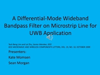
3. Transmission Line Implementation of UWB Filter Port 1 Port 1 Port 2 Port 2 T-Line System DM Setup T-Line System CM Setup Term Term Port 1’ Port 1’ Port 2’ Port 2’ Term Term
4. Varying Design Parameter of T-Line Implementation System Specs: Z1 = 30.1 Ω Z2 = 24.1 Ω Z12 = 49 Ω ZA = 100 Ω Line Length: λg/4
7. Relative Dielectric: 10.8Fullwave simulation results closely match those for the simulated transmission line implementation
8.
9. 20 dB common-mode rejection shown with simulations and through experimentationComparison of fullwave simulation and experimental results using fabricated design over frequency range of 1 to 8 GHz
10. Conclusions Wideband DM bandpass filter designed and fabricated on microstrip 65% DM fractional bandwidth while maintaining 20 dB rejection in CM Theory of model developed using simulations on ideal transmission lines Final microstrip design tested and optimized using fullwave simulator
Editor's Notes
I now introduce the transmission line representation of the filter that this group designed using transmission line theory. Initially, the circuit shown here was designed to have an ultra wide band bandpass filter response in differential mode. The group then added to their design by including two open circuited stubs labeled LA on this plot. In differential mode, there is an effective electrical wall along the horizontal line of symmetry. This electrical wall creates virtual short circuits along this line which results in the figure shown here where the added open circuited stubs are electrically shorted. As you can see, this circuit becomes a simple short circuited bandpass filter design in differential mode. When connected in common mode, the circuit effectively becomes a variable length open circuited stub filter, which results in a bandstop response.
Now that the circuit was designed using transmission line theory, this group simulated their design using an ADS tool. Using this tool, parameters of the open circuited stubs were varied to find how the common mode bandstop response would be affected. The system specifications for the other transmission lines are given here where all the lengths are equal to lambda g over four where lambda g is the guided wavelength of the relevant microstrip line. To start off, this group varied the lengths of the open circuited stubs to find how those lengths affected the bandstop response in common mode. As described in the last slide, the differential mode response in unaffected by any variations to the open circuited stubs. This figure shows that as the length LA is increased, the fractional bandwidth of the common mode bandstop response also increases and at the same time, the rejection skirts become sharper. Now if you look at this figure shown here, the fractional bandwidth of the bandstop response decreases as the impedances of the open circuited stubs increases. The main idea is that using these open circuited stubs, the characteristics of the common mode bandstop response can be controlled.
After simulating the design using ideal transmission lines the group then modeled the filter using microstrip. The open circuited stubs marked La were equally divided folded in to save space. The microstrip design was then simulated using a fullwave simulator. As you can see from the figure, the response is very similar to that of the ideal t-line implementation, with a passband response for the differential mode and a bandreject for the common mode. There is a common mode suppression of a little more than 20 decibels.
After making final modifications to the microstrip design using the fullwave simulator, the UWB bandpass filter was then fabricated as shown here. Experimental data for the fabricated design was collected and compared to the fullwave simulation data shown on the last slide. As you can see, the experimental data for the common and differential modes closely match the responses from the fullwave simulation. The passband ranges from 2.7 to 5.3 GHz with a fractional bandwidth of 65%. There is also more than a 20 decibel common mode rejection which was desired.
To conclude, a wideband differential mode bandpass filter was designed for ultra wide band applications and fabricated on microstrip. The bandpass filter has a 65% fraction bandwidth for the differential mode while maintaining a 20 decibel rejection in the common mode. The theory for this model was first implemented with ideal transmission lines; once the theory was confirmed for this design, it was then implemented in microstrip and tested with a fullwave simulator to optimize the final design.