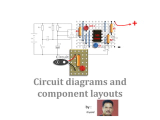
SlideShare a Scribd company logo
1 of 82
+ LED 1 + R1 R3 R2 - + C1 555 timer Circuit diagrams and component layouts by : Krysaid
Circuit Symbols
Circuit Symbols Wires and connections Wire Wires not joined Wires joined Copyright All Right Reserved 2009 : kry... Studio
Circuit Symbols Power Supplies Battery - + Cell DC supply Copyright All Right Reserved 2009 : kry... Studio
Circuit Symbols Power Supplies AC supply ~ Fuse Earth(Ground) Copyright All Right Reserved 2009 : kry... Studio
Circuit Symbols Switches Push Switch(push-to-make) Push-to-Break Switch On-Off Switch(SPST) 2-way Switch/On-on(SPDT) Copyright All Right Reserved 2009 : kry... Studio
Circuit Symbols 2-way Switch/On-on(SPDT) Switches NC COM NO Copyright All Right Reserved 2009 : kry... Studio
Circuit Symbols Resistors Resistor Rheostat Potentiometer Preset Copyright All Right Reserved 2009 : kry... Studio
Circuit Symbols Capacitors Capacitor Capacitor, polarised Variable  Capacitor Trimmer Capacitor + Copyright All Right Reserved 2009 : kry... Studio
Circuit Symbols Diodes LEDLight Emitting Diode Photodiode Zener Diode Diode Copyright All Right Reserved 2009 : kry... Studio
Circuit Symbols Meters Digital Multimeter Analogue Multimeter Voltmeter Galvanometer Ammeter Ohmmeter V A Ω Copyright All Right Reserved 2009 : kry... Studio
Circuit Symbols Output Devices Lamp  (indicator) Lamp  (lighting) Buzzer Motor M Copyright All Right Reserved 2009 : kry... Studio
Circuit Symbols Audio Microphone Earphone Loudspeaker Amplifier(general symbol) Copyright All Right Reserved 2009 : kry... Studio
Circuit Symbols Transistors Transistor NPN Transistor PNP Phototransistor Copyright All Right Reserved 2009 : kry... Studio
Circuit Symbols Sensors (input devices) LDR  Light Dependent Resistor Thermistor Copyright All Right Reserved 2009 : kry... Studio
Circuit Symbols Integrated Circuits (Chips) IC M66T Melody IC IC 555 Timer IC IC 741 Operational Amplifier  8  4  7  7  2  2  6  1  3  6  3  4  3  5  1  2 Copyright All Right Reserved 2009 : kry... Studio
Circuit Diagrams
Examples of Circuit symbols Cell Switch Resistor LED Capacitor Wires Not Joined Wires Joined
+ + 6V 6V Drawing circuit diagrams  The electronics way ( + at the top )  The science way ( battery at the top )
S1 LED 1 1M 33k 8 4 2 555 timer 100k 9V 3 6 7 1 470Ω 220µF LED 2 0.1µF Circuit Diagram + S1 1M LED 1 X + + 33k LED 2 555 100k X 1 8 X 2 7 X 9V 3 6 470Ω Bleeper 0.1µF X 4 5 + 220µF - Component Layout
Verobod
Placing components on Verobod
component verobod Copper tracks
Copper tracks verobod component
Designing a Verobod Layout
LUKISAN BERGAMBAR [litarverobod] Tips: ,[object Object]
Putuskan track diantara pin IC dantandakan [ X ] padagambarajah IC.
Gunakansaiz grid sebenarveroboddisebelahkiriuntukmemeriksajarakkomponen.
Sentiasautamakankeselamatan.Saiz grid sebenarverobod.  Jaraklubang 0.1" (2.54mm) Arusbergeraksecaramendatar 1 2 3 4 5 6 7 8 9 10 11 12 13 14 15 16 17 18 19 20 21 22 23 24 25 26 27 28 29 30 31 32 33 34 35 36 37 38 39 40 41 42 43 44 22 22 21 21 20 20 19 19 18 18 17 17 16 16 15 15 14 14 13 13 12 12 11 11 10 10 9 9 8 8 7 7 6 6 5 5 4 4 3 3 2 2 1 1 1 2 3 4 5 6 7 8 9 10 11 12 13 14 15 16 17 18 19 20 21 22 23 24 25 26 27 28 29 30 31 32 33 34 35 36 37 38 39 40 41 42 43 44  [78/02]   2009 © Hakcipta Krysaid@yahoo.com.my
Planning the Layout 1
R1 9V LED 1 Circuit Diagram
Tips: ,[object Object]
Putuskan track diantara pin IC dantandakan [ X ] padagambarajah IC.
Gunakansaiz grid sebenarveroboddisebelahkiriuntukmemeriksajarakkomponen.
Sentiasautamakankeselamatan.Saiz grid sebenarverobod.  Jaraklubang 0.1" (2.54mm) Arusbergeraksecaramendatar 22 21 20 19 18 1 2 3 4 5 6 7 8 9 10 11 12 13 14 15 16 17 18 19 20 21 22 23 24 25 26 27 28 29 30 31 32 33 34 35 36 37 38 39 40 41 42 43 44 17 22 16 21 15 20 14 19 + 13 18 12 17 11 16 R1 470Ω 10 15 9 14 + 8 LED 13 7 12 BC 6 11 _ 5 10 4 9 3 8 2 7 1 6 5 4 3 2 1 1 2 3 4 5 6 7 8 9 10 11 12 13 14 15 16 17 18 19 20 21 22 23 24 25 26 27 28 29 30 31 32 33 34 35 36 37 38 39 40 41 42 43 44  [78/02]   2009 © Hakcipta Krysaid@yahoo.com.my
Planning the Layout Improve your plan Copyright All Right Reserved 2009 : kry... Studio
Tips: ,[object Object]
Putuskan track diantara pin IC dantandakan [ X ] padagambarajah IC.
Gunakansaiz grid sebenarveroboddisebelahkiriuntukmemeriksajarakkomponen.
Sentiasautamakankeselamatan.Saiz grid sebenarverobod.  Jaraklubang 0.1" (2.54mm) Arusbergeraksecaramendatar 22 21 20 19 18 1 2 3 4 5 6 7 8 9 10 11 12 13 14 15 16 17 18 19 20 21 22 23 24 25 26 27 28 29 30 31 32 33 34 35 36 37 38 39 40 41 42 43 44 17 22 16 21 15 20 14 19 + 13 18 12 17 11 16 R1 470Ω 10 15 9 14 + 8 LED 13 7 12 BC 6 11 _ 5 10 4 9 3 8 2 7 1 6 5 4 3 2 1 1 2 3 4 5 6 7 8 9 10 11 12 13 14 15 16 17 18 19 20 21 22 23 24 25 26 27 28 29 30 31 32 33 34 35 36 37 38 39 40 41 42 43 44  [78/02]   2009 © Hakcipta Krysaid@yahoo.com.my
Planning the Layout Check your plan Copyright All Right Reserved 2009 : kry... Studio
R1 470Ω 9V R1 470Ω LED 1 Circuit Diagram + BC LED
Planning the Layout 2
R 1 S1 LED 1 c 9V b TR 1 R 2 e Circuit Diagram
+ R1 S1 + R2 c LED 1 b e TR 1 _ Tips: ,[object Object]
Putuskan track diantara pin IC dantandakan [ X ] padagambarajah IC.
Gunakansaiz grid sebenarveroboddisebelahkiriuntukmemeriksajarakkomponen.
Sentiasautamakankeselamatan.Saiz grid sebenarverobod.  Jarak lubang 0.1" (2.54mm) Arus bergerak secara mendatar 1 2 3 4 5 6 7 8 9 10 11 12 13 14 15 16 17 18 19 20 21 22 23 24 25 26 27 28 29 30 31 32 33 34 35 36 37 38 39 40 41 42 43 44 22 22 21 21 20 20 19 19 18 18 17 17 16 16 15 15 14 14 13 13 12 12 11 11 10 10 9 9 8 8 7 7 6 6 5 5 4 4 3 3 2 2 1 1 1 2 3 4 5 6 7 8 9 10 11 12 13 14 15 16 17 18 19 20 21 22 23 24 25 26 27 28 29 30 31 32 33 34 35 36 37 38 39 40 41 42 43 44  [78/02]   2009 © Hakcipta Krysaid@yahoo.com.my
Planning the Layout Improve your plan Copyright All Right Reserved 2009 : kry... Studio
+ R1 S1 + R2 c LED 1 b e TR 1 _ Tips: ,[object Object]
Putuskan track diantara pin IC dantandakan [ X ] padagambarajah IC.
Gunakansaiz grid sebenarveroboddisebelahkiriuntukmemeriksajarakkomponen.
Sentiasautamakankeselamatan.Saiz grid sebenarverobod.  Jarak lubang 0.1" (2.54mm) Arus bergerak secara mendatar 1 2 3 4 5 6 7 8 9 10 11 12 13 14 15 16 17 18 19 20 21 22 23 24 25 26 27 28 29 30 31 32 33 34 35 36 37 38 39 40 41 42 43 44 22 22 21 21 20 20 19 19 18 18 17 17 16 16 15 15 14 14 13 13 12 12 11 11 10 10 9 9 8 8 7 7 6 6 5 5 4 4 3 3 2 2 1 1 1 2 3 4 5 6 7 8 9 10 11 12 13 14 15 16 17 18 19 20 21 22 23 24 25 26 27 28 29 30 31 32 33 34 35 36 37 38 39 40 41 42 43 44  [78/02]   2009 © Hakcipta Krysaid@yahoo.com.my
Planning the Layout Check your plan Copyright All Right Reserved 2009 : kry... Studio
R 1 S1 LED 1 c 9V b TR 1 R 2 e R1 Circuit Diagram S1 R2 LED 1 c BC b e TR 1
Planning the Layout 3
R 1 S1 LED 1 R 2 c b TR 2 9V e c b TR 1 e Circuit Diagram
Tips: ,[object Object]
Putuskan track diantara pin IC dantandakan [ X ] padagambarajah IC.
Gunakansaiz grid sebenarveroboddisebelahkiriuntukmemeriksajarakkomponen.
Sentiasautamakankeselamatan.Saiz grid sebenarverobod.  Jarak lubang 0.1" (2.54mm) Arus bergerak secara mendatar + R1 S1 R2 + e b c c LED 1 TR 2 b BC e TR 1 _  [78/02]   2009 © Hakcipta Krysaid@yahoo.com.my     1 2 3 4 5 6 7 8 9 10 11 12 13 14 15 16 17 18 19 20 21 22 23 24 25 26 27 28 29 30 31 32 33 34 35 36 37 38 39 40 41 42 43 44 22 22 21 21 20 20 19 19 18 18 17 17 16 16 15 15 14 14 13 13 12 12 11 11 10 10 9 9 8 8 7 7 6 6 5 5 4 4 3 3 2 2 1 1 1 2 3 4 5 6 7 8 9 10 11 12 13 14 15 16 17 18 19 20 21 22 23 24 25 26 27 28 29 30 31 32 33 34 35 36 37 38 39 40 41 42 43 44
Planning the Layout Improve your plan Copyright All Right Reserved 2009 : kry... Studio
Tips: ,[object Object]
Putuskan track diantara pin IC dantandakan [ X ] padagambarajah IC.
Gunakansaiz grid sebenarveroboddisebelahkiriuntukmemeriksajarakkomponen.
Sentiasautamakankeselamatan.Saiz grid sebenarverobod.  Jarak lubang 0.1" (2.54mm) Arus bergerak secara mendatar + R1 S1 R2 + e b c c LED 1 TR 2 b BC e TR 1 _  [78/02]   2009 © Hakcipta Krysaid@yahoo.com.my     1 2 3 4 5 6 7 8 9 10 11 12 13 14 15 16 17 18 19 20 21 22 23 24 25 26 27 28 29 30 31 32 33 34 35 36 37 38 39 40 41 42 43 44 22 22 21 21 20 20 19 19 18 18 17 17 16 16 15 15 14 14 13 13 12 12 11 11 10 10 9 9 8 8 7 7 6 6 5 5 4 4 3 3 2 2 1 1 1 2 3 4 5 6 7 8 9 10 11 12 13 14 15 16 17 18 19 20 21 22 23 24 25 26 27 28 29 30 31 32 33 34 35 36 37 38 39 40 41 42 43 44
Planning the Layout Check your plan Copyright All Right Reserved 2009 : kry... Studio
R 1 S1 LED 1 R 2 c b TR 2 9V R1 e c S1 b R2 TR 1 + e b e c LED 1 Circuit Diagram TR 2 c b BC e TR 1
Planning the Layout 4
R1 680k 8 4 7 555 timer 9V 6 3 R2 10k R3 1k 2 1 + + C1 10µF LED Circuit Diagram
Tips: ,[object Object]
Putuskan track diantara pin IC dantandakan [ X ] padagambarajah IC.
Gunakansaiz grid sebenarveroboddisebelahkiriuntukmemeriksajarakkomponen.
Sentiasautamakankeselamatan.Saiz grid sebenarverobod.  Jaraklubang 0.1" (2.54mm) Arusbergeraksecaramendatar 22 21 20 19 18 1 2 3 4 5 6 7 8 9 10 11 12 13 14 15 16 17 18 19 20 21 22 23 24 25 26 27 28 29 30 31 32 33 34 35 36 37 38 39 40 41 42 43 44 17 22 16 21 15 20 14 19 + 13 18 12 17 11 16 R1 680k + 10 LED 1 15 R3 1k 9 14 X 1 8 8 13 X 2 7 7 12 X 3 6 6 11 R2 10k X 4 5 5 10 IC 555 4 9 _ 3 C1 10µF 8 + 2 7 1 6 5 4 3 2 1 1 2 3 4 5 6 7 8 9 10 11 12 13 14 15 16 17 18 19 20 21 22 23 24 25 26 27 287 29 30 31 32 33 34 35 36 37 38 39 40 41 42 43 44  [78/02]   2009 © Hakcipta Krysaid@yahoo.com.my
Planning the Layout Improve your plan Copyright All Right Reserved 2009 : kry... Studio
Tips: ,[object Object]
Putuskan track diantara pin IC dantandakan [ X ] padagambarajah IC.
Gunakansaiz grid sebenarveroboddisebelahkiriuntukmemeriksajarakkomponen.
Sentiasautamakankeselamatan.Saiz grid sebenarverobod.  Jaraklubang 0.1" (2.54mm) Arusbergeraksecaramendatar 22 21 20 19 18 1 2 3 4 5 6 7 8 9 10 11 12 13 14 15 16 17 18 19 20 21 22 23 24 25 26 27 28 29 30 31 32 33 34 35 36 37 38 39 40 41 42 43 44 17 22 16 21 15 20 14 19 + 13 18 12 17 11 16 R1 680k + 10 LED 1 15 9 14 R3 1k X 1 8 8 13 X 2 7 7 12 X 3 6 6 11 R2 10k X 4 5 5 10 IC 555 4 9 _ 3 8 C1 10µF + 2 7 1 6 5 4 3 2 1 1 2 3 4 5 6 7 8 9 10 11 12 13 14 15 16 17 18 19 20 21 22 23 24 25 26 27 287 29 30 31 32 33 34 35 36 37 38 39 40 41 42 43 44  [78/02]   2009 © Hakcipta Krysaid@yahoo.com.my
Planning the Layout Check your plan Copyright All Right Reserved 2009 : kry... Studio
R1 680k 8 4 7 555 timer 9V 6 3 R2 10k 555 timer R1 680k + R3 1k 2 LED 1 1 R3 1k X 1 8 + + X 2 7 C1 10µF LED X 3 6 R2 10k X 4 5 IC 555 Circuit Diagram C1 10µF +

More Related Content

Viewers also liked

Wednesday - A Wild Encounter - God Is Unpredictable
Wednesday -  A  Wild  Encounter - God Is  UnpredictableWednesday -  A  Wild  Encounter - God Is  Unpredictable
Wednesday - A Wild Encounter - God Is Unpredictable
Jason Loveless
 
Amazingbeautifullandscapes 090611232859 Phpapp02
Amazingbeautifullandscapes 090611232859 Phpapp02Amazingbeautifullandscapes 090611232859 Phpapp02
Amazingbeautifullandscapes 090611232859 Phpapp02
fauzanmuslim
 
Como escribir un plan de mercado
Como escribir  un plan de mercadoComo escribir  un plan de mercado
Como escribir un plan de mercado
campir
 
The ABC's of Dad and Me
The ABC's of Dad and MeThe ABC's of Dad and Me
The ABC's of Dad and Me
sunnymel20
 
Introduction To Axialent
Introduction To AxialentIntroduction To Axialent
Introduction To Axialent
markburrell
 

Viewers also liked (20)

Wednesday - A Wild Encounter - God Is Unpredictable
Wednesday -  A  Wild  Encounter - God Is  UnpredictableWednesday -  A  Wild  Encounter - God Is  Unpredictable
Wednesday - A Wild Encounter - God Is Unpredictable
 
Social media let's party
Social media let's partySocial media let's party
Social media let's party
 
PPT母版_简约_v0.1
PPT母版_简约_v0.1PPT母版_简约_v0.1
PPT母版_简约_v0.1
 
Amazingbeautifullandscapes 090611232859 Phpapp02
Amazingbeautifullandscapes 090611232859 Phpapp02Amazingbeautifullandscapes 090611232859 Phpapp02
Amazingbeautifullandscapes 090611232859 Phpapp02
 
Facebook Dorkbot
Facebook DorkbotFacebook Dorkbot
Facebook Dorkbot
 
Digital Native
Digital NativeDigital Native
Digital Native
 
normativa minedu
normativa minedu normativa minedu
normativa minedu
 
Thrift
ThriftThrift
Thrift
 
Como escribir un plan de mercado
Como escribir  un plan de mercadoComo escribir  un plan de mercado
Como escribir un plan de mercado
 
The Scientific Method on the Semantic Web
The Scientific Method on the Semantic WebThe Scientific Method on the Semantic Web
The Scientific Method on the Semantic Web
 
Intro
IntroIntro
Intro
 
Crew documents 020549 - 020563
Crew documents 020549 - 020563Crew documents 020549 - 020563
Crew documents 020549 - 020563
 
SEMINARIO 2008
SEMINARIO 2008SEMINARIO 2008
SEMINARIO 2008
 
Why Choose My Sensei
Why Choose My SenseiWhy Choose My Sensei
Why Choose My Sensei
 
The ABC's of Dad and Me
The ABC's of Dad and MeThe ABC's of Dad and Me
The ABC's of Dad and Me
 
BDM Brochure
BDM BrochureBDM Brochure
BDM Brochure
 
Bluebeauty 2
Bluebeauty 2Bluebeauty 2
Bluebeauty 2
 
Social Story Roshen
Social Story   RoshenSocial Story   Roshen
Social Story Roshen
 
Introduction To Axialent
Introduction To AxialentIntroduction To Axialent
Introduction To Axialent
 
Chase Oaks VBX - Tuesday - The Trials Of The Journey
Chase Oaks VBX - Tuesday - The  Trials Of The JourneyChase Oaks VBX - Tuesday - The  Trials Of The Journey
Chase Oaks VBX - Tuesday - The Trials Of The Journey
 

Similar to Circuit Diagrams And Component Layouts

MICROPROCESSOR BASED SUN TRACKING SOLAR PANEL SYSTEM TO MAXIMIZE ENERGY GENER...
MICROPROCESSOR BASED SUN TRACKING SOLAR PANEL SYSTEM TO MAXIMIZE ENERGY GENER...MICROPROCESSOR BASED SUN TRACKING SOLAR PANEL SYSTEM TO MAXIMIZE ENERGY GENER...
MICROPROCESSOR BASED SUN TRACKING SOLAR PANEL SYSTEM TO MAXIMIZE ENERGY GENER...
moiz89
 
2013 06 tdr measurement and simulation of rg58 coaxial cable s-parameters_final
2013 06 tdr measurement and simulation  of rg58 coaxial cable s-parameters_final2013 06 tdr measurement and simulation  of rg58 coaxial cable s-parameters_final
2013 06 tdr measurement and simulation of rg58 coaxial cable s-parameters_final
Piero Belforte
 
Menterjemah Lukisan Skematik
Menterjemah Lukisan SkematikMenterjemah Lukisan Skematik
Menterjemah Lukisan Skematik
Kry Said
 

Similar to Circuit Diagrams And Component Layouts (20)

Receiving card mrv300 specifications v2.1.1
Receiving card mrv300 specifications v2.1.1Receiving card mrv300 specifications v2.1.1
Receiving card mrv300 specifications v2.1.1
 
Understanding panel drive, gamma, mlg
Understanding panel drive, gamma, mlgUnderstanding panel drive, gamma, mlg
Understanding panel drive, gamma, mlg
 
8 x8m guide
8 x8m guide8 x8m guide
8 x8m guide
 
ET&T 5th sem. diploma in eing. Cadd file 2-10 experimants opsahu
 ET&T 5th sem. diploma in eing. Cadd file  2-10 experimants opsahu ET&T 5th sem. diploma in eing. Cadd file  2-10 experimants opsahu
ET&T 5th sem. diploma in eing. Cadd file 2-10 experimants opsahu
 
CSEduino - Build your Arduino from scratch
CSEduino - Build your Arduino from scratchCSEduino - Build your Arduino from scratch
CSEduino - Build your Arduino from scratch
 
Three dimensional integrated circuit
Three dimensional integrated circuitThree dimensional integrated circuit
Three dimensional integrated circuit
 
TE Connectivity: Card Edge Interconnects
TE Connectivity: Card Edge InterconnectsTE Connectivity: Card Edge Interconnects
TE Connectivity: Card Edge Interconnects
 
LG CRT TV MODEL Ct 21q92ke
LG CRT TV MODEL Ct 21q92keLG CRT TV MODEL Ct 21q92ke
LG CRT TV MODEL Ct 21q92ke
 
Hp dv6 7000 goya balen 11254-3
Hp dv6 7000 goya balen 11254-3Hp dv6 7000 goya balen 11254-3
Hp dv6 7000 goya balen 11254-3
 
OpenIot & ELC Europe 2016 Berlin - How to develop the ARM 64bit board, Samsun...
OpenIot & ELC Europe 2016 Berlin - How to develop the ARM 64bit board, Samsun...OpenIot & ELC Europe 2016 Berlin - How to develop the ARM 64bit board, Samsun...
OpenIot & ELC Europe 2016 Berlin - How to develop the ARM 64bit board, Samsun...
 
Netzer ds 247-128-specsheet
Netzer ds 247-128-specsheetNetzer ds 247-128-specsheet
Netzer ds 247-128-specsheet
 
snake game
snake gamesnake game
snake game
 
Netzer ds 58-specsheet
Netzer ds 58-specsheetNetzer ds 58-specsheet
Netzer ds 58-specsheet
 
Netzer ds 25-specsheet
Netzer ds 25-specsheetNetzer ds 25-specsheet
Netzer ds 25-specsheet
 
Simulation-Iss4
Simulation-Iss4Simulation-Iss4
Simulation-Iss4
 
MICROPROCESSOR BASED SUN TRACKING SOLAR PANEL SYSTEM TO MAXIMIZE ENERGY GENER...
MICROPROCESSOR BASED SUN TRACKING SOLAR PANEL SYSTEM TO MAXIMIZE ENERGY GENER...MICROPROCESSOR BASED SUN TRACKING SOLAR PANEL SYSTEM TO MAXIMIZE ENERGY GENER...
MICROPROCESSOR BASED SUN TRACKING SOLAR PANEL SYSTEM TO MAXIMIZE ENERGY GENER...
 
2013 06 tdr measurement and simulation of rg58 coaxial cable s-parameters_final
2013 06 tdr measurement and simulation  of rg58 coaxial cable s-parameters_final2013 06 tdr measurement and simulation  of rg58 coaxial cable s-parameters_final
2013 06 tdr measurement and simulation of rg58 coaxial cable s-parameters_final
 
Menterjemah Lukisan Skematik
Menterjemah Lukisan SkematikMenterjemah Lukisan Skematik
Menterjemah Lukisan Skematik
 
Arduino esc2.0
Arduino esc2.0Arduino esc2.0
Arduino esc2.0
 
Circuitos Digitales - Circuito Digital Sumador
Circuitos Digitales - Circuito Digital SumadorCircuitos Digitales - Circuito Digital Sumador
Circuitos Digitales - Circuito Digital Sumador
 

Recently uploaded

Artificial Intelligence: Facts and Myths
Artificial Intelligence: Facts and MythsArtificial Intelligence: Facts and Myths
Artificial Intelligence: Facts and Myths
Joaquim Jorge
 

Recently uploaded (20)

Bajaj Allianz Life Insurance Company - Insurer Innovation Award 2024
Bajaj Allianz Life Insurance Company - Insurer Innovation Award 2024Bajaj Allianz Life Insurance Company - Insurer Innovation Award 2024
Bajaj Allianz Life Insurance Company - Insurer Innovation Award 2024
 
Artificial Intelligence: Facts and Myths
Artificial Intelligence: Facts and MythsArtificial Intelligence: Facts and Myths
Artificial Intelligence: Facts and Myths
 
Driving Behavioral Change for Information Management through Data-Driven Gree...
Driving Behavioral Change for Information Management through Data-Driven Gree...Driving Behavioral Change for Information Management through Data-Driven Gree...
Driving Behavioral Change for Information Management through Data-Driven Gree...
 
Advantages of Hiring UIUX Design Service Providers for Your Business
Advantages of Hiring UIUX Design Service Providers for Your BusinessAdvantages of Hiring UIUX Design Service Providers for Your Business
Advantages of Hiring UIUX Design Service Providers for Your Business
 
How to convert PDF to text with Nanonets
How to convert PDF to text with NanonetsHow to convert PDF to text with Nanonets
How to convert PDF to text with Nanonets
 
08448380779 Call Girls In Diplomatic Enclave Women Seeking Men
08448380779 Call Girls In Diplomatic Enclave Women Seeking Men08448380779 Call Girls In Diplomatic Enclave Women Seeking Men
08448380779 Call Girls In Diplomatic Enclave Women Seeking Men
 
From Event to Action: Accelerate Your Decision Making with Real-Time Automation
From Event to Action: Accelerate Your Decision Making with Real-Time AutomationFrom Event to Action: Accelerate Your Decision Making with Real-Time Automation
From Event to Action: Accelerate Your Decision Making with Real-Time Automation
 
Real Time Object Detection Using Open CV
Real Time Object Detection Using Open CVReal Time Object Detection Using Open CV
Real Time Object Detection Using Open CV
 
GenCyber Cyber Security Day Presentation
GenCyber Cyber Security Day PresentationGenCyber Cyber Security Day Presentation
GenCyber Cyber Security Day Presentation
 
Handwritten Text Recognition for manuscripts and early printed texts
Handwritten Text Recognition for manuscripts and early printed textsHandwritten Text Recognition for manuscripts and early printed texts
Handwritten Text Recognition for manuscripts and early printed texts
 
Mastering MySQL Database Architecture: Deep Dive into MySQL Shell and MySQL R...
Mastering MySQL Database Architecture: Deep Dive into MySQL Shell and MySQL R...Mastering MySQL Database Architecture: Deep Dive into MySQL Shell and MySQL R...
Mastering MySQL Database Architecture: Deep Dive into MySQL Shell and MySQL R...
 
Exploring the Future Potential of AI-Enabled Smartphone Processors
Exploring the Future Potential of AI-Enabled Smartphone ProcessorsExploring the Future Potential of AI-Enabled Smartphone Processors
Exploring the Future Potential of AI-Enabled Smartphone Processors
 
Presentation on how to chat with PDF using ChatGPT code interpreter
Presentation on how to chat with PDF using ChatGPT code interpreterPresentation on how to chat with PDF using ChatGPT code interpreter
Presentation on how to chat with PDF using ChatGPT code interpreter
 
Understanding Discord NSFW Servers A Guide for Responsible Users.pdf
Understanding Discord NSFW Servers A Guide for Responsible Users.pdfUnderstanding Discord NSFW Servers A Guide for Responsible Users.pdf
Understanding Discord NSFW Servers A Guide for Responsible Users.pdf
 
The 7 Things I Know About Cyber Security After 25 Years | April 2024
The 7 Things I Know About Cyber Security After 25 Years | April 2024The 7 Things I Know About Cyber Security After 25 Years | April 2024
The 7 Things I Know About Cyber Security After 25 Years | April 2024
 
The Role of Taxonomy and Ontology in Semantic Layers - Heather Hedden.pdf
The Role of Taxonomy and Ontology in Semantic Layers - Heather Hedden.pdfThe Role of Taxonomy and Ontology in Semantic Layers - Heather Hedden.pdf
The Role of Taxonomy and Ontology in Semantic Layers - Heather Hedden.pdf
 
Slack Application Development 101 Slides
Slack Application Development 101 SlidesSlack Application Development 101 Slides
Slack Application Development 101 Slides
 
Workshop - Best of Both Worlds_ Combine KG and Vector search for enhanced R...
Workshop - Best of Both Worlds_ Combine  KG and Vector search for  enhanced R...Workshop - Best of Both Worlds_ Combine  KG and Vector search for  enhanced R...
Workshop - Best of Both Worlds_ Combine KG and Vector search for enhanced R...
 
A Year of the Servo Reboot: Where Are We Now?
A Year of the Servo Reboot: Where Are We Now?A Year of the Servo Reboot: Where Are We Now?
A Year of the Servo Reboot: Where Are We Now?
 
Breaking the Kubernetes Kill Chain: Host Path Mount
Breaking the Kubernetes Kill Chain: Host Path MountBreaking the Kubernetes Kill Chain: Host Path Mount
Breaking the Kubernetes Kill Chain: Host Path Mount
 

Circuit Diagrams And Component Layouts

  • 1. + LED 1 + R1 R3 R2 - + C1 555 timer Circuit diagrams and component layouts by : Krysaid
  • 3. Circuit Symbols Wires and connections Wire Wires not joined Wires joined Copyright All Right Reserved 2009 : kry... Studio
  • 4. Circuit Symbols Power Supplies Battery - + Cell DC supply Copyright All Right Reserved 2009 : kry... Studio
  • 5. Circuit Symbols Power Supplies AC supply ~ Fuse Earth(Ground) Copyright All Right Reserved 2009 : kry... Studio
  • 6. Circuit Symbols Switches Push Switch(push-to-make) Push-to-Break Switch On-Off Switch(SPST) 2-way Switch/On-on(SPDT) Copyright All Right Reserved 2009 : kry... Studio
  • 7. Circuit Symbols 2-way Switch/On-on(SPDT) Switches NC COM NO Copyright All Right Reserved 2009 : kry... Studio
  • 8. Circuit Symbols Resistors Resistor Rheostat Potentiometer Preset Copyright All Right Reserved 2009 : kry... Studio
  • 9. Circuit Symbols Capacitors Capacitor Capacitor, polarised Variable  Capacitor Trimmer Capacitor + Copyright All Right Reserved 2009 : kry... Studio
  • 10. Circuit Symbols Diodes LEDLight Emitting Diode Photodiode Zener Diode Diode Copyright All Right Reserved 2009 : kry... Studio
  • 11. Circuit Symbols Meters Digital Multimeter Analogue Multimeter Voltmeter Galvanometer Ammeter Ohmmeter V A Ω Copyright All Right Reserved 2009 : kry... Studio
  • 12. Circuit Symbols Output Devices Lamp  (indicator) Lamp  (lighting) Buzzer Motor M Copyright All Right Reserved 2009 : kry... Studio
  • 13. Circuit Symbols Audio Microphone Earphone Loudspeaker Amplifier(general symbol) Copyright All Right Reserved 2009 : kry... Studio
  • 14. Circuit Symbols Transistors Transistor NPN Transistor PNP Phototransistor Copyright All Right Reserved 2009 : kry... Studio
  • 15. Circuit Symbols Sensors (input devices) LDR Light Dependent Resistor Thermistor Copyright All Right Reserved 2009 : kry... Studio
  • 16. Circuit Symbols Integrated Circuits (Chips) IC M66T Melody IC IC 555 Timer IC IC 741 Operational Amplifier 8 4 7 7 2 2 6 1 3 6 3 4 3 5 1 2 Copyright All Right Reserved 2009 : kry... Studio
  • 18. Examples of Circuit symbols Cell Switch Resistor LED Capacitor Wires Not Joined Wires Joined
  • 19. + + 6V 6V Drawing circuit diagrams The electronics way ( + at the top ) The science way ( battery at the top )
  • 20. S1 LED 1 1M 33k 8 4 2 555 timer 100k 9V 3 6 7 1 470Ω 220µF LED 2 0.1µF Circuit Diagram + S1 1M LED 1 X + + 33k LED 2 555 100k X 1 8 X 2 7 X 9V 3 6 470Ω Bleeper 0.1µF X 4 5 + 220µF - Component Layout
  • 26.
  • 27. Putuskan track diantara pin IC dantandakan [ X ] padagambarajah IC.
  • 29. Sentiasautamakankeselamatan.Saiz grid sebenarverobod. Jaraklubang 0.1" (2.54mm) Arusbergeraksecaramendatar 1 2 3 4 5 6 7 8 9 10 11 12 13 14 15 16 17 18 19 20 21 22 23 24 25 26 27 28 29 30 31 32 33 34 35 36 37 38 39 40 41 42 43 44 22 22 21 21 20 20 19 19 18 18 17 17 16 16 15 15 14 14 13 13 12 12 11 11 10 10 9 9 8 8 7 7 6 6 5 5 4 4 3 3 2 2 1 1 1 2 3 4 5 6 7 8 9 10 11 12 13 14 15 16 17 18 19 20 21 22 23 24 25 26 27 28 29 30 31 32 33 34 35 36 37 38 39 40 41 42 43 44 [78/02] 2009 © Hakcipta Krysaid@yahoo.com.my
  • 31. R1 9V LED 1 Circuit Diagram
  • 32.
  • 33. Putuskan track diantara pin IC dantandakan [ X ] padagambarajah IC.
  • 35. Sentiasautamakankeselamatan.Saiz grid sebenarverobod. Jaraklubang 0.1" (2.54mm) Arusbergeraksecaramendatar 22 21 20 19 18 1 2 3 4 5 6 7 8 9 10 11 12 13 14 15 16 17 18 19 20 21 22 23 24 25 26 27 28 29 30 31 32 33 34 35 36 37 38 39 40 41 42 43 44 17 22 16 21 15 20 14 19 + 13 18 12 17 11 16 R1 470Ω 10 15 9 14 + 8 LED 13 7 12 BC 6 11 _ 5 10 4 9 3 8 2 7 1 6 5 4 3 2 1 1 2 3 4 5 6 7 8 9 10 11 12 13 14 15 16 17 18 19 20 21 22 23 24 25 26 27 28 29 30 31 32 33 34 35 36 37 38 39 40 41 42 43 44 [78/02] 2009 © Hakcipta Krysaid@yahoo.com.my
  • 36. Planning the Layout Improve your plan Copyright All Right Reserved 2009 : kry... Studio
  • 37.
  • 38. Putuskan track diantara pin IC dantandakan [ X ] padagambarajah IC.
  • 40. Sentiasautamakankeselamatan.Saiz grid sebenarverobod. Jaraklubang 0.1" (2.54mm) Arusbergeraksecaramendatar 22 21 20 19 18 1 2 3 4 5 6 7 8 9 10 11 12 13 14 15 16 17 18 19 20 21 22 23 24 25 26 27 28 29 30 31 32 33 34 35 36 37 38 39 40 41 42 43 44 17 22 16 21 15 20 14 19 + 13 18 12 17 11 16 R1 470Ω 10 15 9 14 + 8 LED 13 7 12 BC 6 11 _ 5 10 4 9 3 8 2 7 1 6 5 4 3 2 1 1 2 3 4 5 6 7 8 9 10 11 12 13 14 15 16 17 18 19 20 21 22 23 24 25 26 27 28 29 30 31 32 33 34 35 36 37 38 39 40 41 42 43 44 [78/02] 2009 © Hakcipta Krysaid@yahoo.com.my
  • 41. Planning the Layout Check your plan Copyright All Right Reserved 2009 : kry... Studio
  • 42. R1 470Ω 9V R1 470Ω LED 1 Circuit Diagram + BC LED
  • 44. R 1 S1 LED 1 c 9V b TR 1 R 2 e Circuit Diagram
  • 45.
  • 46. Putuskan track diantara pin IC dantandakan [ X ] padagambarajah IC.
  • 48. Sentiasautamakankeselamatan.Saiz grid sebenarverobod. Jarak lubang 0.1" (2.54mm) Arus bergerak secara mendatar 1 2 3 4 5 6 7 8 9 10 11 12 13 14 15 16 17 18 19 20 21 22 23 24 25 26 27 28 29 30 31 32 33 34 35 36 37 38 39 40 41 42 43 44 22 22 21 21 20 20 19 19 18 18 17 17 16 16 15 15 14 14 13 13 12 12 11 11 10 10 9 9 8 8 7 7 6 6 5 5 4 4 3 3 2 2 1 1 1 2 3 4 5 6 7 8 9 10 11 12 13 14 15 16 17 18 19 20 21 22 23 24 25 26 27 28 29 30 31 32 33 34 35 36 37 38 39 40 41 42 43 44 [78/02] 2009 © Hakcipta Krysaid@yahoo.com.my
  • 49. Planning the Layout Improve your plan Copyright All Right Reserved 2009 : kry... Studio
  • 50.
  • 51. Putuskan track diantara pin IC dantandakan [ X ] padagambarajah IC.
  • 53. Sentiasautamakankeselamatan.Saiz grid sebenarverobod. Jarak lubang 0.1" (2.54mm) Arus bergerak secara mendatar 1 2 3 4 5 6 7 8 9 10 11 12 13 14 15 16 17 18 19 20 21 22 23 24 25 26 27 28 29 30 31 32 33 34 35 36 37 38 39 40 41 42 43 44 22 22 21 21 20 20 19 19 18 18 17 17 16 16 15 15 14 14 13 13 12 12 11 11 10 10 9 9 8 8 7 7 6 6 5 5 4 4 3 3 2 2 1 1 1 2 3 4 5 6 7 8 9 10 11 12 13 14 15 16 17 18 19 20 21 22 23 24 25 26 27 28 29 30 31 32 33 34 35 36 37 38 39 40 41 42 43 44 [78/02] 2009 © Hakcipta Krysaid@yahoo.com.my
  • 54. Planning the Layout Check your plan Copyright All Right Reserved 2009 : kry... Studio
  • 55. R 1 S1 LED 1 c 9V b TR 1 R 2 e R1 Circuit Diagram S1 R2 LED 1 c BC b e TR 1
  • 57. R 1 S1 LED 1 R 2 c b TR 2 9V e c b TR 1 e Circuit Diagram
  • 58.
  • 59. Putuskan track diantara pin IC dantandakan [ X ] padagambarajah IC.
  • 61. Sentiasautamakankeselamatan.Saiz grid sebenarverobod. Jarak lubang 0.1" (2.54mm) Arus bergerak secara mendatar + R1 S1 R2 + e b c c LED 1 TR 2 b BC e TR 1 _ [78/02] 2009 © Hakcipta Krysaid@yahoo.com.my 1 2 3 4 5 6 7 8 9 10 11 12 13 14 15 16 17 18 19 20 21 22 23 24 25 26 27 28 29 30 31 32 33 34 35 36 37 38 39 40 41 42 43 44 22 22 21 21 20 20 19 19 18 18 17 17 16 16 15 15 14 14 13 13 12 12 11 11 10 10 9 9 8 8 7 7 6 6 5 5 4 4 3 3 2 2 1 1 1 2 3 4 5 6 7 8 9 10 11 12 13 14 15 16 17 18 19 20 21 22 23 24 25 26 27 28 29 30 31 32 33 34 35 36 37 38 39 40 41 42 43 44
  • 62. Planning the Layout Improve your plan Copyright All Right Reserved 2009 : kry... Studio
  • 63.
  • 64. Putuskan track diantara pin IC dantandakan [ X ] padagambarajah IC.
  • 66. Sentiasautamakankeselamatan.Saiz grid sebenarverobod. Jarak lubang 0.1" (2.54mm) Arus bergerak secara mendatar + R1 S1 R2 + e b c c LED 1 TR 2 b BC e TR 1 _ [78/02] 2009 © Hakcipta Krysaid@yahoo.com.my 1 2 3 4 5 6 7 8 9 10 11 12 13 14 15 16 17 18 19 20 21 22 23 24 25 26 27 28 29 30 31 32 33 34 35 36 37 38 39 40 41 42 43 44 22 22 21 21 20 20 19 19 18 18 17 17 16 16 15 15 14 14 13 13 12 12 11 11 10 10 9 9 8 8 7 7 6 6 5 5 4 4 3 3 2 2 1 1 1 2 3 4 5 6 7 8 9 10 11 12 13 14 15 16 17 18 19 20 21 22 23 24 25 26 27 28 29 30 31 32 33 34 35 36 37 38 39 40 41 42 43 44
  • 67. Planning the Layout Check your plan Copyright All Right Reserved 2009 : kry... Studio
  • 68. R 1 S1 LED 1 R 2 c b TR 2 9V R1 e c S1 b R2 TR 1 + e b e c LED 1 Circuit Diagram TR 2 c b BC e TR 1
  • 70. R1 680k 8 4 7 555 timer 9V 6 3 R2 10k R3 1k 2 1 + + C1 10µF LED Circuit Diagram
  • 71.
  • 72. Putuskan track diantara pin IC dantandakan [ X ] padagambarajah IC.
  • 74. Sentiasautamakankeselamatan.Saiz grid sebenarverobod. Jaraklubang 0.1" (2.54mm) Arusbergeraksecaramendatar 22 21 20 19 18 1 2 3 4 5 6 7 8 9 10 11 12 13 14 15 16 17 18 19 20 21 22 23 24 25 26 27 28 29 30 31 32 33 34 35 36 37 38 39 40 41 42 43 44 17 22 16 21 15 20 14 19 + 13 18 12 17 11 16 R1 680k + 10 LED 1 15 R3 1k 9 14 X 1 8 8 13 X 2 7 7 12 X 3 6 6 11 R2 10k X 4 5 5 10 IC 555 4 9 _ 3 C1 10µF 8 + 2 7 1 6 5 4 3 2 1 1 2 3 4 5 6 7 8 9 10 11 12 13 14 15 16 17 18 19 20 21 22 23 24 25 26 27 287 29 30 31 32 33 34 35 36 37 38 39 40 41 42 43 44 [78/02] 2009 © Hakcipta Krysaid@yahoo.com.my
  • 75. Planning the Layout Improve your plan Copyright All Right Reserved 2009 : kry... Studio
  • 76.
  • 77. Putuskan track diantara pin IC dantandakan [ X ] padagambarajah IC.
  • 79. Sentiasautamakankeselamatan.Saiz grid sebenarverobod. Jaraklubang 0.1" (2.54mm) Arusbergeraksecaramendatar 22 21 20 19 18 1 2 3 4 5 6 7 8 9 10 11 12 13 14 15 16 17 18 19 20 21 22 23 24 25 26 27 28 29 30 31 32 33 34 35 36 37 38 39 40 41 42 43 44 17 22 16 21 15 20 14 19 + 13 18 12 17 11 16 R1 680k + 10 LED 1 15 9 14 R3 1k X 1 8 8 13 X 2 7 7 12 X 3 6 6 11 R2 10k X 4 5 5 10 IC 555 4 9 _ 3 8 C1 10µF + 2 7 1 6 5 4 3 2 1 1 2 3 4 5 6 7 8 9 10 11 12 13 14 15 16 17 18 19 20 21 22 23 24 25 26 27 287 29 30 31 32 33 34 35 36 37 38 39 40 41 42 43 44 [78/02] 2009 © Hakcipta Krysaid@yahoo.com.my
  • 80. Planning the Layout Check your plan Copyright All Right Reserved 2009 : kry... Studio
  • 81. R1 680k 8 4 7 555 timer 9V 6 3 R2 10k 555 timer R1 680k + R3 1k 2 LED 1 1 R3 1k X 1 8 + + X 2 7 C1 10µF LED X 3 6 R2 10k X 4 5 IC 555 Circuit Diagram C1 10µF +
  • 82.
  • 84. + 9V LED 1 R1 R2 8 4 6 R3 IC 555 7 3 R4 2 1 + C1 LED 2 S1 - 0V Circuit Diagram
  • 85.
  • 86. Putuskan track diantara pin IC dantandakan [ X ] padagambarajah IC.
  • 88. Sentiasautamakankeselamatan.Saiz grid sebenarverobod. Jaraklubang 0.1" (2.54mm) Arusbergeraksecaramendatar 1 2 3 4 5 6 7 8 9 10 11 12 13 14 15 16 17 18 19 20 21 22 23 24 25 26 27 28 29 30 31 32 33 34 35 36 37 38 39 40 41 42 43 44 22 22 21 21 20 20 19 19 18 18 17 17 16 16 15 15 14 14 LED 1 LED 2 13 13 12 + 12 + 11 11 10 10 R1 R2 9 9 8 8 X 1 8 7 7 X S1 2 7 6 6 X BC + 3 6 5 5 X R4 R3 4 5 4 C1 4 IC 555 3 3 2 2 + 1 1 1 2 3 4 5 6 7 8 9 10 11 12 13 14 15 16 17 18 19 20 21 22 23 24 25 26 27 28 29 30 31 32 33 34 35 36 37 38 39 40 41 42 43 44 _ [78/02] 2009 © Hakcipta Krysaid@yahoo.com.my
  • 89. Planning the Layout Improve your plan Copyright All Right Reserved 2009 : kry... Studio
  • 90.
  • 91. Putuskan track diantara pin IC dantandakan [ X ] padagambarajah IC.
  • 93. Sentiasautamakankeselamatan.Saiz grid sebenarverobod. Jaraklubang 0.1" (2.54mm) Arusbergeraksecaramendatar 1 2 3 4 5 6 7 8 9 10 11 12 13 14 15 16 17 18 19 20 21 22 23 24 25 26 27 28 29 30 31 32 33 34 35 36 37 38 39 40 41 42 43 44 22 22 21 21 20 20 19 19 18 18 17 17 16 16 15 15 14 14 LED 1 13 13 12 + 12 LED 2 + 11 11 10 10 R1 R2 9 9 8 8 X 1 8 7 7 X S1 2 7 6 6 X BC + 3 6 5 5 X R4 4 5 4 C1 4 IC 555 3 3 R3 2 2 + 1 1 1 2 3 4 5 6 7 8 9 10 11 12 13 14 15 16 17 18 19 20 21 22 23 24 25 26 27 28 29 30 31 32 33 34 35 36 37 38 39 40 41 42 43 44 _ [78/02] 2009 © Hakcipta Krysaid@yahoo.com.my
  • 94. Planning the Layout Check your plan Copyright All Right Reserved 2009 : kry... Studio
  • 95. + 9V LED 1 R1 R2 8 4 6 R3 LED 1 IC 555 7 3 + LED 2 + 555 timer R4 2 R1 1 R5 X + 1 8 X S1 2 7 C1 LED 2 S1 X BC 3 6 X R4 4 5 - 0V C1 Circuit Diagram IC 555 R3 +
  • 97. S1 LED 1 R1 33k 1M 8 4 2 R3 100k 555 timer 9V 3 6 R2 470Ω 7 1 C1 220µF C2 0.1µF LED 2 Circuit Diagram
  • 98. Saiz grid sebenarverobod. Jaraklubang 0.1" (2.54mm) Arusbergeraksecaramendatar 1 2 3 4 5 6 7 8 9 10 11 12 13 14 15 16 17 18 19 20 21 22 23 24 25 26 27 28 29 30 31 32 33 34 35 36 37 38 39 40 41 42 43 44 22 22 21 21 20 20 19 19 18 18 17 17 16 16 S1 15 15 1M 14 14 + LED 1 LED 2 13 13 X 12 + 12 11 + 11 10 10 R1 33k 9 9 IC 555 8 R3 100k 8 X 1 8 7 7 X 2 7 6 6 X 9V 3 6 BZ 5 5 X 4 5 + C2 0.1µF 4 C1 220µF 4 _ 3 3 R2 470Ω 2 2 1 1 1 2 3 4 5 6 7 8 9 10 11 12 13 14 15 16 17 18 19 20 21 22 23 24 25 26 27 28 29 30 31 32 33 34 35 36 37 38 39 40 41 42 43 44 [78/02] 2009 © Hakcipta Krysaid@yahoo.com.my
  • 99. Planning the Layout Improve your plan Copyright All Right Reserved 2009 : kry... Studio
  • 100. Saiz grid sebenarverobod. Jaraklubang 0.1" (2.54mm) Arusbergeraksecaramendatar 1 2 3 4 5 6 7 8 9 10 11 12 13 14 15 16 17 18 19 20 21 22 23 24 25 26 27 28 29 30 31 32 33 34 35 36 37 38 39 40 41 42 43 44 22 22 21 21 20 20 19 19 18 18 17 17 16 16 S1 15 15 1M 14 14 + LED 1 LED 2 13 13 X 12 + 12 11 + 11 10 10 R1 33k 9 9 IC 555 8 R3 100k 8 X 1 8 7 7 X 2 7 6 6 X 9V 3 6 BZ 5 5 X 4 5 + C2 0.1µF 4 C1 220µF 4 _ 3 3 R2 470Ω 2 2 1 1 1 2 3 4 5 6 7 8 9 10 11 12 13 14 15 16 17 18 19 20 21 22 23 24 25 26 27 28 29 30 31 32 33 34 35 36 37 38 39 40 41 42 43 44 [78/02] 2009 © Hakcipta Krysaid@yahoo.com.my
  • 101. Planning the Layout Check your plan Copyright All Right Reserved 2009 : kry... Studio
  • 102. S1 1M LED 2 LED 1 X + + 555 timer + + R1 33k IC 555 R3 100k X 1 8 X 2 7 X 9V 3 6 BZ X 4 5 + + C2 0.1µF C1 220µF R2 470Ω
  • 104. R1 R2 R6 8 4 7 IC 555 R5 6 3 2 1 5 5 C2 1 LS 2 9V IC Muzik 1 R3 R4 NO NC 3 C1 c S1 b COM LED e TR Circuit Diagram
  • 105. Saiz grid sebenarverobod. Jaraklubang 0.1" (2.54mm) Arusbergeraksecaramendatar 22 21 20 19 18 1 2 3 4 5 6 7 8 9 10 11 12 13 14 15 16 17 18 19 20 21 22 23 24 25 26 27 28 29 30 31 32 33 34 35 36 37 38 39 40 41 42 43 44 17 22 16 21 15 20 + 14 19 13 18 12 17 R1 11 16 NC R2 R6 10 15 NO 9 COM 14 X C2 8 1 8 BC 13 X 7 2 7 12 X 6 3 6 11 R5 X 5 4 5 R3 10 4 1 IC 555 R4 9 + X C1 3 2 8 _ 2 c 3 + 7 1 b IC Muzik 6 e 5 LED TR 4 3 2 1 1 2 3 4 5 6 7 8 9 10 11 12 13 14 15 16 17 18 19 20 21 22 23 24 25 26 27 28 29 30 31 32 33 34 35 36 37 38 39 40 41 42 43 44 [78/02] 2009 © Hakcipta Krysaid@yahoo.com.my [78/02] 2009 © Hakcipta Krysaid@yahoo.com.my
  • 106. Planning the Layout Improve your plan Copyright All Right Reserved 2009 : kry... Studio
  • 107. Saiz grid sebenarverobod. Jaraklubang 0.1" (2.54mm) Arusbergeraksecaramendatar 22 21 20 19 18 1 2 3 4 5 6 7 8 9 10 11 12 13 14 15 16 17 18 19 20 21 22 23 24 25 26 27 28 29 30 31 32 33 34 35 36 37 38 39 40 41 42 43 44 17 22 16 21 15 20 + 14 19 13 18 12 17 R1 11 16 NC R2 R6 10 15 NO 9 COM 14 X C2 8 1 8 13 X 7 2 7 12 BC X 6 3 6 11 R5 X 5 4 5 R3 10 9V 4 1 IC 555 R4 9 + X C1 3 2 8 _ 2 c 3 + 7 1 b IC Muzik 6 e 5 LED TR 4 3 2 1 1 2 3 4 5 6 7 8 9 10 11 12 13 14 15 16 17 18 19 20 21 22 23 24 25 26 27 28 29 30 31 32 33 34 35 36 37 38 39 40 41 42 43 44 [78/02] 2009 © Hakcipta Krysaid@yahoo.com.my [78/02] 2009 © Hakcipta Krysaid@yahoo.com.my
  • 108. Planning the Layout Check your plan Copyright All Right Reserved 2009 : kry... Studio
  • 109. 555 timer R1 R6 R2 NO BC NO COM COM C2 X 1 8 X 2 7 R3 X 3 6 X R5 4 5 LS IC 555 1 R4 + C1 X 2 c 3 + LED IC Muzik b e TR
  • 111. S1 R1 LS 1 2 LED 2 LED 1 3 IC Muzik R2 R3 1 9V + + C2 C1 C C b b e e Circuit Diagram
  • 112. Saiz grid sebenarverobod. Jaraklubang 0.1" (2.54mm) Arusbergeraksecaramendatar 1 2 3 4 5 6 7 8 9 10 11 12 13 14 15 16 17 18 19 20 21 22 23 24 25 26 27 28 29 30 31 32 33 34 35 36 37 38 39 40 41 42 43 44 22 22 21 21 20 20 19 19 18 18 17 17 16 16 15 15 14 14 13 13 12 12 11 11 10 10 9 9 8 8 7 7 6 6 5 5 4 4 3 3 2 2 1 1 1 2 3 4 5 6 7 8 9 10 11 12 13 14 15 16 17 18 19 20 21 22 23 24 25 26 27 28 29 30 31 32 33 34 35 36 37 38 39 40 41 42 43 44 [78/02] 2009 © Hakcipta Krysaid@yahoo.com.my
  • 114. S1 R2 10k R3 10k R5 10k R6 10k R8 1k C3 1µF 8 4 8 4 C1 0.1µF C2 0.1µF 555 timer 555 timer 3 3 2 2 9V 3 R4 470Ω R1 470Ω S4 S3 6 1 6 1 S2 Buzer R7 1k Circuit Diagram
  • 115. Saiz grid sebenarverobod. Jaraklubang 0.1" (2.54mm) Arusbergeraksecaramendatar 1 2 3 4 5 6 7 8 9 10 11 12 13 14 15 16 17 18 19 20 21 22 23 24 25 26 27 28 29 30 31 32 33 34 35 36 37 38 39 40 41 42 43 44 22 22 21 21 20 20 19 19 18 18 17 17 16 16 15 15 14 14 13 13 12 12 11 11 10 10 9 9 8 8 7 7 6 6 5 5 4 4 3 3 2 2 1 1 1 2 3 4 5 6 7 8 9 10 11 12 13 14 15 16 17 18 19 20 21 22 23 24 25 26 27 28 29 30 31 32 33 34 35 36 37 38 39 40 41 42 43 44 [78/02] 2009 © Hakcipta Krysaid@yahoo.com.my