HAND TOOLS USED AT ELECTRONICS WORK PRESENTED BY KOUSTAV SARKAR
Pic16 c505
1. 1999-2012 Microchip Technology Inc. DS40192D-page 1
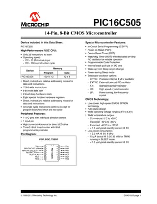
Device included in this Data Sheet:
PIC16C505
High-Performance RISC CPU:
• Only 33 instructions to learn
• Operating speed:
- DC - 20 MHz clock input
- DC - 200 ns instruction cycle
• Direct, indirect and relative addressing modes for
data and instructions
• 12-bit wide instructions
• 8-bit wide data path
• 2-level deep hardware stack
• Eight special function hardware registers
• Direct, indirect and relative addressing modes for
data and instructions
• All single cycle instructions (200 ns) except for
program branches which are two-cycle
Peripheral Features:
• 11 I/O pins with individual direction control
• 1 input pin
• High current sink/source for direct LED drive
• Timer0: 8-bit timer/counter with 8-bit
programmable prescaler
Pin Diagram:
Device
Memory
Program Data
PIC16C505 1024 x 12 72 x 8
PDIP, SOIC, TSSOP
PIC16C505
VDD
RB5/OSC1/CLKIN
RB4/OSC2/CLKOUT
RB3/MCLR/VPP
RC5/T0CKI
RC4
RC3
VSS
RB0
RB1
RB2
RC0
RC1
RC2
1
2
3
4
5
6
7
14
13
12
11
10
9
8
Special Microcontroller Features:
• In-Circuit Serial Programming (ICSP™)
• Power-on Reset (POR)
• Device Reset Timer (DRT)
• Watchdog Timer (WDT) with dedicated on-chip
RC oscillator for reliable operation
• Programmable Code Protection
• Internal weak pull-ups on I/O pins
• Wake-up from Sleep on pin change
• Power-saving Sleep mode
• Selectable oscillator options:
- INTRC: Precision internal 4 MHz oscillator
- EXTRC: External low-cost RC oscillator
- XT: Standard crystal/resonator
- HS: High speed crystal/resonator
- LP: Power saving, low frequency
crystal
CMOS Technology:
• Low-power, high-speed CMOS EPROM
technology
• Fully static design
• Wide operating voltage range (2.5V to 5.5V)
• Wide temperature ranges
- Commercial: 0°C to +70°C
- Industrial: -40°C to +85°C
- Extended: -40°C to +125°C
- < 1.0 A typical standby current @ 5V
• Low power consumption
- < 2.0 mA @ 5V, 4 MHz
- 15 A typical @ 3.0V, 32 kHz for TMR0
running in SLEEP mode
- < 1.0 A typical standby current @ 5V
PIC16C505
14-Pin, 8-Bit CMOS Microcontroller
2. PIC16C505
DS40192D-page 2 1999-2012 Microchip Technology Inc.
TABLE OF CONTENTS
1.0 General Description..................................................................................................................................................................... 3
2.0 PIC16C505 Device Varieties....................................................................................................................................................... 5
3.0 Architectural Overview ................................................................................................................................................................ 7
4.0 Memory Organization ................................................................................................................................................................ 11
5.0 I/O Port ...................................................................................................................................................................................... 19
6.0 Timer0 Module and TMR0 Register .......................................................................................................................................... 23
7.0 Special Features of the CPU..................................................................................................................................................... 27
8.0 Instruction Set Summary ........................................................................................................................................................... 39
9.0 Development Support................................................................................................................................................................ 51
10.0 Electrical Characteristics - PIC16C505 ..................................................................................................................................... 55
11.0 DC and AC Characteristics - PIC16C505.................................................................................................................................. 69
12.0 Packaging Information............................................................................................................................................................... 73
PIC16C505 Product Identification System .......................................................................................................................................... 87
TO OUR VALUED CUSTOMERS
It is our intention to provide our valued customers with the best documentation possible to ensure successful use of your Microchip
products. To this end, we will continue to improve our publications to better suit your needs. Our publications will be refined and
enhanced as new volumes and updates are introduced.
If you have any questions or comments regarding this publication, please contact the Marketing Communications Department via
E-mail at docerrors@microchip.com or fax the Reader Response Form in the back of this data sheet to (480) 792-4150. We
welcome your feedback.
Most Current Data Sheet
To obtain the most up-to-date version of this data sheet, please register at our Worldwide Web site at:
http://www.microchip.com
You can determine the version of a data sheet by examining its literature number found on the bottom outside corner of any page.
The last character of the literature number is the version number, (e.g., DS30000A is version A of document DS30000).
Errata
An errata sheet, describing minor operational differences from the data sheet and recommended workarounds, may exist for current
devices. As device/documentation issues become known to us, we will publish an errata sheet. The errata will specify the revision
of silicon and revision of document to which it applies.
To determine if an errata sheet exists for a particular device, please check with one of the following:
• Microchip’s Worldwide Web site; http://www.microchip.com
• Your local Microchip sales office (see last page)
When contacting a sales office, please specify which device, revision of silicon and data sheet (include literature number) you are
using.
Customer Notification System
Register on our web site at www.microchip.com to receive the most current information on all of our products.
3. 1999-2012 Microchip Technology Inc. DS40192D-page 3
PIC16C505
1.0 GENERAL DESCRIPTION
The PIC16C505 from Microchip Technology is a low-
cost, high-performance, 8-bit, fully static, EPROM/
ROM-based CMOS microcontroller. It employs a RISC
architecture with only 33 single word/single cycle
instructions. All instructions are single cycle (200 s)
except for program branches, which take two cycles.
The PIC16C505 delivers performance an order of mag-
nitude higher than its competitors in the same price cat-
egory. The 12-bit wide instructions are highly
symmetrical resulting in a typical 2:1 code compression
over other 8-bit microcontrollers in its class. The easy
to use and easy to remember instruction set reduces
development time significantly.
The PIC16C505 product is equipped with special fea-
tures that reduce system cost and power requirements.
The Power-On Reset (POR) and Device Reset Timer
(DRT) eliminate the need for external reset circuitry.
There are five oscillator configurations to choose from,
including INTRC internal oscillator mode and the
power-saving LP (Low Power) oscillator mode. Power
saving SLEEP mode, Watchdog Timer and code
protection features improve system cost, power and
reliability.
The PIC16C505 is available in the cost-effective One-
Time-Programmable (OTP) version, which is suitable
for production in any volume. The customer can take
full advantage of Microchip’s price leadership in OTP
microcontrollers, while benefiting from the OTP’s
flexibility.
The PIC16C505 product is supported by a full-featured
macro assembler, a software simulator, an in-circuit
emulator, a ‘C’ compiler, a low-cost development pro-
grammer and a full featured programmer. All the tools
are supported on IBM
PC and compatible machines.
1.1 Applications
The PIC16C505 fits in applications ranging from per-
sonal care appliances and security systems to low-
power remote transmitters/receivers. The EPROM
technology makes customizing application programs
(transmitter codes, appliance settings, receiver fre-
quencies, etc.) extremely fast and convenient. The
small footprint packages, for through hole or surface
mounting, make this microcontroller perfect for applica-
tions with space limitations. Low-cost, low-power, high-
performance, ease of use and I/O flexibility make the
PIC16C505 very versatile even in areas where no
microcontroller use has been considered before (e.g.,
timer functions, replacement of “glue” logic and PLD’s
in larger systems, and coprocessor applications).
4. PIC16C505
DS40192D-page 4 1999-2012 Microchip Technology Inc.
TABLE 1-1: PIC16C505 DEVICE
PIC16C505
Clock
Maximum Frequency
of Operation (MHz)
20
Memory
EPROM Program Memory 1024
Data Memory (bytes) 72
Peripherals
Timer Module(s) TMR0
Wake-up from SLEEP on
pin change
Yes
Features
I/O Pins 11
Input Pins 1
Internal Pull-ups Yes
In-Circuit Serial Programming Yes
Number of Instructions 33
Packages 14-pin DIP, SOIC, TSSOP
The PIC16C505 device has Power-on Reset, selectable Watchdog Timer, selectable code protect, high I/O current capability and
precision internal oscillator.
The PIC16C505 device uses serial programming with data pin RB0 and clock pin RB1.
5. 1999-2012 Microchip Technology Inc. DS40192D-page 5
PIC16C505
2.0 PIC16C505 DEVICE VARIETIES
A variety of packaging options are available.
Depending on application and production
requirements, the proper device option can be
selected using the information in this section. When
placing orders, please use the PIC16C505 Product
Identification System at the back of this data sheet to
specify the correct part number.
2.1 One-Time-Programmable (OTP)
Devices
The availability of OTP devices is especially useful for
customers who need the flexibility of frequent code
updates or small volume applications.
The OTP devices, packaged in plastic packages, per-
mit the user to program them once. In addition to the
program memory, the configuration bits must also be
programmed.
2.2 Quick-Turnaround-Production (QTP)
Devices
Microchip offers a QTP Programming Service for
factory production orders. This service is made
available for users who choose not to program medium
to high quantity units and whose code patterns have
stabilized. The devices are identical to the OTP devices
but with all EPROM locations and fuse options already
programmed by the factory. Certain code and prototype
verification procedures do apply before production
shipments are available. Please contact your local
Microchip Technology sales office for more details.
2.3 Serialized Quick-Turnaround
Production (SQTPSM) Devices
Microchip offers a unique programming service, where
a few user-defined locations in each device are
programmed with different serial numbers. The serial
numbers may be random, pseudo-random or
sequential.
Serial programming allows each device to have a
unique number, which can serve as an entry-code,
password or ID number.
7. 1999-2012 Microchip Technology Inc. DS40192D-page 7
PIC16C505
3.0 ARCHITECTURAL OVERVIEW
The high performance of the PIC16C505 can be
attributed to a number of architectural features
commonly found in RISC microprocessors. To begin
with, the PIC16C505 uses a Harvard architecture in
which program and data are accessed on separate
buses. This improves bandwidth over traditional von
Neumann architecture where program and data are
fetched on the same bus. Separating program and
data memory further allows instructions to be sized
differently than the 8-bit wide data word. Instruction
opcodes are 12 bits wide, making it possible to have
all single word instructions. A 12-bit wide program
memory access bus fetches a 12-bit instruction in a
single cycle. A two-stage pipeline overlaps fetch and
execution of instructions. Consequently, all instructions
(33) execute in a single cycle (200ns @ 20MHz)
except for program branches.
The Table below lists program memory (EPROM) and
data memory (RAM) for the PIC16C505.
The PIC16C505 can directly or indirectly address its
register files and data memory. All special function
registers, including the program counter, are mapped
in the data memory. The PIC16C505 has a highly
orthogonal (symmetrical) instruction set that makes it
possible to carry out any operation on any register
using any addressing mode. This symmetrical nature
and lack of ‘special optimal situations’ make
programming with the PIC16C505 simple yet efficient.
In addition, the learning curve is reduced significantly.
Device
Memory
Program Data
PIC16C505 1024 x 12 72 x 8
The PIC16C505 device contains an 8-bit ALU and
working register. The ALU is a general purpose
arithmetic unit. It performs arithmetic and Boolean
functions between data in the working register and any
register file.
The ALU is 8-bits wide and capable of addition,
subtraction, shift and logical operations. Unless
otherwise mentioned, arithmetic operations are two's
complement in nature. In two-operand instructions,
one operand is typically the W (working) register. The
other operand is either a file register or an immediate
constant. In single operand instructions, the operand is
either the W register or a file register.
The W register is an 8-bit working register used for
ALU operations. It is not an addressable register.
Depending on the instruction executed, the ALU may
affect the values of the Carry (C), Digit Carry (DC),
and Zero (Z) bits in the STATUS register. The C and
DC bits operate as a borrow and digit borrow out bit,
respectively, in subtraction. See the SUBWF and ADDWF
instructions for examples.
A simplified block diagram is shown in Figure 3-1, with
the corresponding device pins described in Table 3-1.
8. PIC16C505
DS40192D-page 8 1999-2012 Microchip Technology Inc.
FIGURE 3-1: PIC16C505 BLOCK DIAGRAM
Device Reset
Timer
Power-on
Reset
Watchdog
Timer
EPROM
Program
Memory
12
Data Bus
8
12Program
Bus
Instruction reg
Program Counter
RAM
File
Registers
Direct Addr 5
RAM Addr 9
Addr MUX
Indirect
Addr
FSR reg
STATUS reg
MUX
ALU
W reg
Instruction
Decode &
Control
Timing
Generation
OSC1/CLKIN
OSC2
MCLR
VDD, VSS
Timer0
PORTB
8
8
RB4/OSC2/CLKOUT
RB3/MCLR/VPP
RB2
RB1
RB0
5-7
3
RB5/OSC1/CLKIN
STACK1
STACK2
1K x 12
72 bytes
Internal RC
OSC
PORTC
RC4
RC3
RC2
RC1
RC0
RC5/T0CKI
9. 1999-2012 Microchip Technology Inc. DS40192D-page 9
PIC16C505
TABLE 3-1: PIC16C505 PINOUT DESCRIPTION
Name
DIP
Pin #
SOIC
Pin #
I/O/P
Type
Buffer
Type
Description
RB0 13 13 I/O TTL/ST Bi-directional I/O port/ serial programming data. Can
be software programmed for internal weak pull-up and
wake-up from SLEEP on pin change. This buffer is a
Schmitt Trigger input when used in serial programming
mode.
RB1 12 12 I/O TTL/ST Bi-directional I/O port/ serial programming clock. Can
be software programmed for internal weak pull-up and
wake-up from SLEEP on pin change. This buffer is a
Schmitt Trigger input when used in serial programming
mode.
RB2 11 11 I/O TTL Bi-directional I/O port.
RB3/MCLR/VPP 4 4 I TTL/ST Input port/master clear (reset) input/programming volt-
age input. When configured as MCLR, this pin is an
active low reset to the device. Voltage on MCLR/VPP
must not exceed VDD during normal device operation.
Can be software programmed for internal weak pull-up
and wake-up from SLEEP on pin change. Weak pull-
up only when configured as RB3. ST when configured
as MCLR.
RB4/OSC2/CLKOUT 3 3 I/O TTL Bi-directional I/O port/oscillator crystal output. Con-
nections to crystal or resonator in crystal oscillator
mode (XT and LP modes only, RB4 in other modes).
Can be software programmed for internal weak pull-up
and wake-up from SLEEP on pin change. In EXTRC
and INTRC modes, the pin output can be configured to
CLKOUT, which has 1/4 the frequency of OSC1 and
denotes the instruction cycle rate.
RB5/OSC1/CLKIN 2 2 I/O TTL/ST Bidirectional IO port/oscillator crystal input/external
clock source input (RB5 in Internal RC mode only,
OSC1 in all other oscillator modes). TTL input when
RB5, ST input in external RC oscillator mode.
RC0 10 10 I/O TTL Bi-directional I/O port.
RC1 9 9 I/O TTL Bi-directional I/O port.
RC2 8 8 I/O TTL Bi-directional I/O port.
RC3 7 7 I/O TTL Bi-directional I/O port.
RC4 6 6 I/O TTL Bi-directional I/O port.
RC5/T0CKI 5 5 I/O ST Bi-directional I/O port. Can be configured as T0CKI.
VDD 1 1 P — Positive supply for logic and I/O pins
VSS 14 14 P — Ground reference for logic and I/O pins
Legend: I = input, O = output, I/O = input/output, P = power, — = not used, TTL = TTL input,
ST = Schmitt Trigger input
10. PIC16C505
DS40192D-page 10 1999-2012 Microchip Technology Inc.
3.1 Clocking Scheme/Instruction Cycle
The clock input (OSC1/CLKIN pin) is internally divided
by four to generate four non-overlapping quadrature
clocks namely Q1, Q2, Q3 and Q4. Internally, the
program counter is incremented every Q1, and the
instruction is fetched from program memory and
latched into the instruction register in Q4. It is decoded
and executed during the following Q1 through Q4. The
clocks and instruction execution flow is shown in
Figure 3-2 and Example 3-1.
3.2 Instruction Flow/Pipelining
An Instruction cycle consists of four Q cycles (Q1, Q2,
Q3 and Q4). The instruction fetch and execute are
pipelined such that fetch takes one instruction cycle,
while decode and execute takes another instruction
cycle. However, due to the pipelining, each instruction
effectively executes in one cycle. If an instruction
causes the program counter to change (e.g., GOTO)
then two cycles are required to complete the
instruction (Example 3-1).
A fetch cycle begins with the program counter (PC)
incrementing in Q1.
In the execution cycle, the fetched instruction is
latched into the Instruction Register (IR) in cycle Q1.
This instruction is then decoded and executed during
the Q2, Q3 and Q4 cycles. Data memory is read
during Q2 (operand read) and written during Q4
(destination write).
FIGURE 3-2: CLOCK/INSTRUCTION CYCLE
EXAMPLE 3-1: INSTRUCTION PIPELINE FLOW
Q1 Q2 Q3 Q4 Q1 Q2 Q3 Q4 Q1 Q2 Q3 Q4
OSC1
Q1
Q2
Q3
Q4
PC PC PC+1 PC+2
Fetch INST (PC)
Execute INST (PC-1) Fetch INST (PC+1)
Execute INST (PC) Fetch INST (PC+2)
Execute INST (PC+1)
Internal
phase
clock
All instructions are single cycle, except for any program branches. These take two cycles, since the fetch
instruction is “flushed” from the pipeline, while the new instruction is being fetched and then executed.
1. MOVLW 03H Fetch 1 Execute 1
2. MOVWF PORTB Fetch 2 Execute 2
3. CALL SUB_1 Fetch 3 Execute 3
4. BSF PORTB, BIT1 Fetch 4 Flush
Fetch SUB_1 Execute SUB_1
11. 1999-2012 Microchip Technology Inc. DS40192D-page 11
PIC16C505
4.0 MEMORY ORGANIZATION
PIC16C505 memory is organized into program mem-
ory and data memory. For the PIC16C505, a paging
scheme is used. Program memory pages are
accessed using one STATUS register bit. Data mem-
ory banks are accessed using the File Select Register
(FSR).
4.1 Program Memory Organization
The PIC16C505 devices have a 12-bit Program
Counter (PC).
The 1K x 12 (0000h-03FFh) for the PIC16C505 are
physically implemented. Refer to Figure 4-1.
Accessing a location above this boundary will cause a
wrap-around within the first 1K x 12 space. The
effective reset vector is at 0000h, (see Figure 4-1).
Location 03FFh contains the internal clock oscillator
calibration value. This value should never be
overwritten.
FIGURE 4-1: PROGRAM MEMORY MAP
AND STACK FOR THE
PIC16C505
CALL, RETLW
PC<11:0>
Stack Level 1
Stack Level 2
UserMemory
Space
12
0000h
7FFh
01FFh
0200h
Reset Vector (note 1)
Note 1: Address 0000h becomes the
effective reset vector. Location 03FFh
contains the MOVLW XX INTERNAL RC
oscillator calibration value.
1024 Words 03FFh
0400h
On-chip Program
Memory
12. PIC16C505
DS40192D-page 12 1999-2012 Microchip Technology Inc.
4.2 Data Memory Organization
Data memory is composed of registers or bytes of
RAM. Therefore, data memory for a device is specified
by its register file. The register file is divided into two
functional groups: Special Function Registers and
General Purpose Registers.
The Special Function Registers include the TMR0
register, the Program Counter (PCL), the Status
Register, the I/O registers (ports) and the File Select
Register (FSR). In addition, Special Function
Registers are used to control the I/O port configuration
and prescaler options.
The General Purpose Registers are used for data and
control information under command of the instructions.
For the PIC16C505, the register file is composed of 8
Special Function Registers, 24 General Purpose
Registers and 48 General Purpose Registers that may
be addressed using a banking scheme (Figure 4-2).
4.2.1 GENERAL PURPOSE REGISTER FILE
The General Purpose Register file is accessed, either
directly or indirectly, through the File Select Register
FSR (Section 4.8).
FIGURE 4-2: PIC16C505 REGISTER FILE MAP
File Address
00h
01h
02h
03h
04h
05h
06h
07h
1Fh
INDF(1)
TMR0
PCL
STATUS
FSR
OSCCAL
PORTB
0Fh
10h
Bank 0 Bank 1
3Fh
30h
20h
2Fh
General
Purpose
Registers
General
Purpose
Registers
General
Purpose
Registers
Addresses map back to
addresses in Bank 0.
Note 1: Not a physical register.
FSR<6:5> 00 01
Bank 3
7Fh
70h
60h
6Fh
General
Purpose
Registers
11
Bank 2
5Fh
50h
40h
4Fh
General
Purpose
Registers
10
08h
PORTC
13. 1999-2012 Microchip Technology Inc. DS40192D-page 13
PIC16C505
4.2.2 SPECIAL FUNCTION REGISTERS
The Special Function Registers (SFRs) are registers
used by the CPU and peripheral functions to control
the operation of the device (Table 4-1).
The Special Function Registers can be classified into
two sets. The Special Function Registers associated
with the “core” functions are described in this section.
Those related to the operation of the peripheral
features are described in the section for each
peripheral feature.
TABLE 4-1: SPECIAL FUNCTION REGISTER (SFR) SUMMARY
Address Name Bit 7 Bit 6 Bit 5 Bit 4 Bit 3 Bit 2 Bit 1 Bit 0
Value on
Power-On
Reset
Value on
All Other
Resets(2)
00h INDF Uses contents of FSR to address data memory (not a physical register) xxxx xxxx uuuu uuuu
01h TMR0 8-bit real-time clock/counter xxxx xxxx uuuu uuuu
02h(1) PCL Low order 8 bits of PC 1111 1111 1111 1111
03h STATUS RBWUF — PAO TO PD Z DC C 0001 1xxx q00q quuu(1)
04h FSR Indirect data memory address pointer 110x xxxx 11uu uuuu
05h OSCCAL CAL5 CAL4 CAL3 CAL2 CAL1 CAL0 — — 1000 00-- uuuu uu--
N/A TRISB — — I/O control registers --11 1111 --11 1111
N/A TRISC — — I/O control registers --11 1111 --11 1111
N/A OPTION RBWU RBPU TOCS TOSE PSA PS2 PS1 PS0 1111 1111 1111 1111
06h PORTB — — RB5 RB4 RB3 RB2 RB1 RB0 --xx xxxx --uu uuuu
07h PORTC — — RC5 RC4 RC3 RC2 RC1 RC0 --xx xxxx --uu uuuu
Legend: Shaded cells not used by Port Registers, read as ‘0’, — = unimplemented, read as ‘0’, x = unknown, u = unchanged,
q = depends on condition.
Note 1: If reset was due to wake-up on pin change, then bit 7 = 1. All other rests will cause bit 7 = 0.
Note 2: Other (non-power-up) resets include external reset through MCLR, watchdog timer and wake-up on pin change reset.
14. PIC16C505
DS40192D-page 14 1999-2012 Microchip Technology Inc.
4.3 STATUS Register
This register contains the arithmetic status of the ALU,
the RESET status and the page preselect bit.
The STATUS register can be the destination for any
instruction, as with any other register. If the STATUS
register is the destination for an instruction that affects
the Z, DC or C bits, then the write to these three bits is
disabled. These bits are set or cleared according to
the device logic. Furthermore, the TO and PD bits are
not writable. Therefore, the result of an instruction with
the STATUS register as destination may be different
than intended.
For example, CLRF STATUS will clear the upper three
bits and set the Z bit. This leaves the STATUS register
as 000u u1uu (where u = unchanged).
It is recommended, therefore, that only BCF, BSF and
MOVWF instructions be used to alter the STATUS
register, because these instructions do not affect the
Z, DC or C bits from the STATUS register. For other
instructions, which do affect STATUS bits, see
Instruction Set Summary.
REGISTER 4-1: STATUS REGISTER (ADDRESS:03h)
R/W-0 R/W-0 R/W-0 R-1 R-1 R/W-x R/W-x R/W-x
RBWUF — PA0 TO PD Z DC C R = Readable bit
W = Writable bit
U = Unimplemented bit,
read as ‘0’
- n = Value at POR reset
bit7 6 5 4 3 2 1 bit0
bit 7: RBWUF: I/O reset bit
1 = Reset due to wake-up from SLEEP on pin change
0 = After power up or other reset
bit 6: Unimplemented
bit 5: PA0: Program page preselect bits
1 = Page 1 (200h - 3FFh)
0 = Page 0 (000h - 1FFh)
Each page is 512 bytes.
Using the PA0 bit as a general purpose read/write bit in devices which do not use it for program
page preselect is not recommended, since this may affect upward compatibility with future products.
bit 4: TO: Time-out bit
1 = After power-up, CLRWDT instruction, or SLEEP instruction
0 = A WDT time-out occurred
bit 3: PD: Power-down bit
1 = After power-up or by the CLRWDT instruction
0 = By execution of the SLEEP instruction
bit 2: Z: Zero bit
1 = The result of an arithmetic or logic operation is zero
0 = The result of an arithmetic or logic operation is not zero
bit 1: DC: Digit carry/borrow bit (for ADDWF and SUBWF instructions)
ADDWF
1 = A carry from the 4th low order bit of the result occurred
0 = A carry from the 4th low order bit of the result did not occur
SUBWF
1 = A borrow from the 4th low order bit of the result did not occur
0 = A borrow from the 4th low order bit of the result occurred
bit 0: C: Carry/borrow bit (for ADDWF, SUBWF and RRF, RLF instructions)
ADDWF SUBWF RRF or RLF
1 = A carry occurred 1 = A borrow did not occur Load bit with LSB or MSB, respectively
0 = A carry did not occur 0 = A borrow occurred
15. 1999-2012 Microchip Technology Inc. DS40192D-page 15
PIC16C505
4.4 OPTION Register
The OPTION register is a 8-bit wide, write-only
register, which contains various control bits to
configure the Timer0/WDT prescaler and Timer0.
By executing the OPTION instruction, the contents of
the W register will be transferred to the OPTION
register. A RESET sets the OPTION<7:0> bits.
Note: If TRIS bit is set to ‘0’, the wake-up on
change and pull-up functions are disabled
for that pin (i.e., note that TRIS overrides
OPTION control of RBPU and RBWU).
REGISTER 4-2: OPTION REGISTER
W-1 W-1 W-1 W-1 W-1 W-1 W-1 W-1
RBWU RBPU T0CS T0SE PSA PS2 PS1 PS0 R = Readable bit
W = Writable bit
U = Unimplemented bit,
read as ‘0’
- n = Value at POR reset
bit7 6 5 4 3 2 1 bit0
bit 7: RBWU: Enable wake-up on pin change (RB0, RB1, RB3, RB4)
1 = Disabled
0 = Enabled
bit 6: RBPU: Enable weak pull-ups (RB0, RB1, RB3, RB4)
1 = Disabled
0 = Enabled
bit 5: T0CS: Timer0 clock source select bit
1 = Transition on T0CKI pin (overrides TRIS <RC57>
0 = Transition on internal instruction cycle clock, Fosc/4
bit 4: T0SE: Timer0 source edge select bit
1 = Increment on high to low transition on the T0CKI pin
0 = Increment on low to high transition on the T0CKI pin
bit 3: PSA: Prescaler assignment bit
1 = Prescaler assigned to the WDT
0 = Prescaler assigned to Timer0
bit 2-0: PS<2:0>: Prescaler rate select bits
000
001
010
011
100
101
110
111
1 : 2
1 : 4
1 : 8
1 : 16
1 : 32
1 : 64
1 : 128
1 : 256
1 : 1
1 : 2
1 : 4
1 : 8
1 : 16
1 : 32
1 : 64
1 : 128
Bit Value Timer0 Rate WDT Rate
16. PIC16C505
DS40192D-page 16 1999-2012 Microchip Technology Inc.
4.5 OSCCAL Register
The Oscillator Calibration (OSCCAL) register is used to
calibrate the internal 4 MHz oscillator. It contains six
bits for calibration
After you move in the calibration constant, do not
change the value. See Section 7.2.5
Note: Please note that erasing the device will
also erase the pre-programmed internal
calibration value for the internal oscillator.
The calibration value must be read prior to
erasing the part, so it can be repro-
grammed correctly later.
REGISTER 4-3: OSCCAL REGISTER (ADDRESS 05h) PIC16C505
R/W-1 R/W-0 R/W-0 R/W-0 R/W-0 R/W-0 U-0 U-0
CAL5 CAL4 CAL3 CAL2 CAL1 CAL0 — — R = Readable bit
W = Writable bit
U = Unimplemented bit,
read as ‘0’
- n = Value at POR reset
bit7 bit0
bit 7-2: CAL<5:0>: Calibration
bit 1-0: Unimplemented read as ‘0’
17. 1999-2012 Microchip Technology Inc. DS40192D-page 17
PIC16C505
4.6 Program Counter
As a program instruction is executed, the Program
Counter (PC) will contain the address of the next
program instruction to be executed. The PC value is
increased by one every instruction cycle, unless an
instruction changes the PC.
For a GOTO instruction, bits 8:0 of the PC are provided
by the GOTO instruction word. The PC Latch (PCL) is
mapped to PC<7:0>. Bit 5 of the STATUS register
provides page information to bit 9 of the PC
(Figure 4-3).
For a CALL instruction, or any instruction where the
PCL is the destination, bits 7:0 of the PC again are
provided by the instruction word. However, PC<8>
does not come from the instruction word, but is always
cleared (Figure 4-3).
Instructions where the PCL is the destination, or
Modify PCL instructions, include MOVWF PC, ADDWF
PC, and BSF PC,5.
FIGURE 4-3: LOADING OF PC
BRANCH INSTRUCTIONS -
PIC16C505
Note: Because PC<8> is cleared in the CALL
instruction or any Modify PCL instruction,
all subroutine calls or computed jumps are
limited to the first 256 locations of any pro-
gram memory page (512 words long).
PA0
STATUS
PC
8 7 0
PCL
910
Instruction Word
7 0
GOTO Instruction
CALL or Modify PCL Instruction
11
PA0
STATUS
PC
8 7 0
PCL
910
Instruction Word
7 0
11
Reset to ‘0’
4.6.1 EFFECTS OF RESET
The Program Counter is set upon a RESET, which
means that the PC addresses the last location in the
last page (i.e., the oscillator calibration instruction.)
After executing MOVLW XX, the PC will roll over to
location 00h and begin executing user code.
The STATUS register page preselect bits are cleared
upon a RESET, which means that page 0 is pre-
selected.
Therefore, upon a RESET, a GOTO instruction will
automatically cause the program to jump to page 0
until the value of the page bits is altered.
4.7 Stack
PIC16C505 devices have a 12-bit wide hardware
push/pop stack.
A CALL instruction will push the current value of stack
1 into stack 2 and then push the current program
counter value, incremented by one, into stack level 1. If
more than two sequential CALL’s are executed, only
the most recent two return addresses are stored.
A RETLW instruction will pop the contents of stack level
1 into the program counter and then copy stack level 2
contents into level 1. If more than two sequential
RETLW’s are executed, the stack will be filled with the
address previously stored in level 2. Note that the
W register will be loaded with the literal value specified
in the instruction. This is particularly useful for the
implementation of data look-up tables within the
program memory.
Note 1: There are no STATUS bits to indicate
stack overflows or stack underflow condi-
tions.
Note 2: There are no instructions mnemonics
called PUSH or POP. These are actions that
occur from the execution of the CALL,
RETLW, and instructions.
18. PIC16C505
DS40192D-page 18 1999-2012 Microchip Technology Inc.
4.8 Indirect Data Addressing; INDF and
FSR Registers
The INDF register is not a physical register.
Addressing INDF actually addresses the register
whose address is contained in the FSR register (FSR
is a pointer). This is indirect addressing.
EXAMPLE 4-1: INDIRECT ADDRESSING
• Register file 07 contains the value 10h
• Register file 08 contains the value 0Ah
• Load the value 07 into the FSR register
• A read of the INDF register will return the value
of 10h
• Increment the value of the FSR register by one
(FSR = 08)
• A read of the INDR register now will return the
value of 0Ah.
Reading INDF itself indirectly (FSR = 0) will produce
00h. Writing to the INDF register indirectly results in a
no-operation (although STATUS bits may be affected).
A simple program to clear RAM locations 10h-1Fh
using indirect addressing is shown in Example 4-2.
EXAMPLE 4-2: HOW TO CLEAR RAM
USING INDIRECT
ADDRESSING
movlw 0x10 ;initialize pointer
movwf FSR ; to RAM
NEXT clrf INDF ;clear INDF register
incf FSR,F ;inc pointer
btfsc FSR,4 ;all done?
goto NEXT ;NO, clear next
CONTINUE
: ;YES, continue
:
The FSR is a 5-bit wide register. It is used in
conjunction with the INDF register to indirectly address
the data memory area.
The FSR<4:0> bits are used to select data memory
addresses 00h to 1Fh.
The device uses FSR<6:5> to select between banks
0:3.
FIGURE 4-4: DIRECT/INDIRECT ADDRESSING
Note 1: For register map detail see Section 4.2.
Direct Addressing
(FSR)
6 5 4 (opcode) 0
bank select location select
00 01 10 11
00h
0Fh
10h
Data
Memory(1)
1Fh 3Fh 5Fh 7Fh
Bank 0 Bank 1 Bank 2 Bank 3
Addresses
map back to
addresses
in Bank 0.
Indirect Addressing
6 5 4 (FSR) 0
bank location select
19. 1999-2012 Microchip Technology Inc. DS40192D-page 19
PIC16C505
5.0 I/O PORT
As with any other register, the I/O register can be
written and read under program control. However,
read instructions (e.g., MOVF PORTB,W) always read
the I/O pins independent of the pin’s input/output
modes. On RESET, all I/O ports are defined as input
(inputs are at hi-impedance) since the I/O control
registers are all set.
5.1 PORTB
PORTB is an 8-bit I/O register. Only the low order 6
bits are used (RB<5:0>). Bits 7 and 6 are
unimplemented and read as '0's. Please note that RB3
is an input only pin. The configuration word can set
several I/O’s to alternate functions. When acting as
alternate functions, the pins will read as ‘0’ during port
read. Pins RB0, RB1, RB3 and RB4 can be configured
with weak pull-ups and also with wake-up on change.
The wake-up on change and weak pull-up functions
are not pin selectable. If pin 4 is configured as MCLR,
weak pull-up is always off and wake-up on change for
this pin is not enabled.
5.2 PORTC
PORTC is an 8-bit I/O register. Only the low order 6 bits
are used (RC<5:0>). Bits 7 and 6 are unimplemented
and read as ‘0’s.
5.3 TRIS Registers
The output driver control register is loaded with the
contents of the W register by executing the TRIS f
instruction. A '1' from a TRIS register bit puts the
corresponding output driver in a hi-impedance mode.
A '0' puts the contents of the output data latch on the
selected pins, enabling the output buffer. The
exceptions are RB3, which is input only, and RC5,
which may be controlled by the option register. See
Register 4-2.
The TRIS registers are “write-only” and are set (output
drivers disabled) upon RESET.
Note: A read of the ports reads the pins, not the
output data latches. That is, if an output
driver on a pin is enabled and driven high,
but the external system is holding it low, a
read of the port will indicate that the pin is
low.
5.4 I/O Interfacing
The equivalent circuit for an I/O port pin is shown in
Figure 5-1. All port pins except RB3, which is input
only, may be used for both input and output operations.
For input operations, these ports are non-latching. Any
input must be present until read by an input instruction
(e.g., MOVF PORTB,W). The outputs are latched and
remain unchanged until the output latch is rewritten. To
use a port pin as output, the corresponding direction
control bit in TRIS must be cleared (= 0). For use as an
input, the corresponding TRIS bit must be set. Any I/O
pin (except RB3) can be programmed individually as
input or output.
FIGURE 5-1: EQUIVALENT CIRCUIT
FOR A SINGLE I/O PIN
Data
Bus
QD
QCK
QD
QCK
P
N
WR
Port
TRIS ‘f’
Data
TRIS
RD Port
VSS
VDD
I/O
pin(1)
W
Reg
Latch
Latch
Reset
Note 1: I/O pins have protection diodes to VDD and VSS.
Note 2: See Table 3-1 for buffer type.
(2)
20. PIC16C505
DS40192D-page 20 1999-2012 Microchip Technology Inc.
TABLE 5-1: SUMMARY OF PORT REGISTERS
Address Name Bit 7 Bit 6 Bit 5 Bit 4 Bit 3 Bit 2 Bit 1 Bit 0
Value on
Power-On
Reset
Value on
All Other Resets
N/A TRISB — — I/O control registers --11 1111 --11 1111
N/A TRISC — — I/O control registers --11 1111 --11 1111
N/A OPTION RBWU RBPU TOCS TOSE PSA PS2 PS1 PS0 1111 1111 1111 1111
03h STATUS RBWUF — PAO TO PD Z DC C 0001 1xxx q00q quuu(1)
06h PORTB — — RB5 RB4 RB3 RB2 RB1 RB0 --xx xxxx --uu uuuu
07h PORTC — — RC5 RC4 RC3 RC2 RC1 RC0 --xx xxxx --uu uuuu
Legend: Shaded cells not used by Port Registers, read as ‘0’, — = unimplemented, read as ‘0’, x = unknown, u = unchanged,
q = depends on condition.
Note 1: If reset was due to wake-up on pin change, then bit 7 = 1. All other rests will cause bit 7 = 0.
5.5 I/O Programming Considerations
5.5.1 BI-DIRECTIONAL I/O PORTS
Some instructions operate internally as read followed
by write operations. The BCF and BSF instructions, for
example, read the entire port into the CPU, execute
the bit operation and re-write the result. Caution must
be used when these instructions are applied to a port
where one or more pins are used as input/outputs. For
example, a BSF operation on bit5 of PORTB will cause
all eight bits of PORTB to be read into the CPU, bit5 to
be set and the PORTB value to be written to the output
latches. If another bit of PORTB is used as a bi-
directional I/O pin (say bit0) and it is defined as an
input at this time, the input signal present on the pin
itself would be read into the CPU and rewritten to the
data latch of this particular pin, overwriting the
previous content. As long as the pin stays in the input
mode, no problem occurs. However, if bit0 is switched
into output mode later on, the content of the data latch
may now be unknown.
Example 5-1 shows the effect of two sequential read-
modify-write instructions (e.g., BCF, BSF, etc.) on an
I/O port.
A pin actively outputting a high or a low should not be
driven from external devices at the same time in order
to change the level on this pin (“wired-or”, “wired-
and”). The resulting high output currents may damage
the chip.
EXAMPLE 5-1: READ-MODIFY-WRITE
INSTRUCTIONS ON AN
I/O PORT
;Initial PORTB Settings
; PORTB<5:3> Inputs
; PORTB<2:0> Outputs
;
; PORTB latch PORTB pins
; ---------- ----------
BCF PORTB, 5 ;--01 -ppp --11 pppp
BCF PORTB, 4 ;--10 -ppp --11 pppp
MOVLW 007h ;
TRIS PORTB ;--10 -ppp --11 pppp
;
;Note that the user may have expected the pin
;values to be --00 pppp. The 2nd BCF caused
;RB5 to be latched as the pin value (High).
5.5.2 SUCCESSIVE OPERATIONS ON I/O
PORTS
The actual write to an I/O port happens at the end of
an instruction cycle, whereas for reading, the data
must be valid at the beginning of the instruction cycle
(Figure 5-2). Therefore, care must be exercised if a
write followed by a read operation is carried out on the
same I/O port. The sequence of instructions should
allow the pin voltage to stabilize (load dependent)
before the next instruction causes that file to be read
into the CPU. Otherwise, the previous state of that pin
may be read into the CPU rather than the new state.
When in doubt, it is better to separate these
instructions with a NOP or another instruction not
accessing this I/O port.
21. 1999-2012 Microchip Technology Inc. DS40192D-page 21
PIC16C505
FIGURE 5-2: SUCCESSIVE I/O OPERATION
PC PC + 1 PC + 2 PC + 3
Q1 Q2 Q3 Q4 Q1 Q2 Q3 Q4 Q1 Q2 Q3 Q4 Q1 Q2 Q3 Q4
Instruction
fetched
RB<5:0>
MOVWF PORTB NOP
Port pin
sampled here
NOPMOVF PORTB,W
Instruction
executed MOVWF PORTB
(Write to PORTB)
NOPMOVF PORTB,W
This example shows a write to PORTB
followed by a read from PORTB.
Data setup time = (0.25 TCY – TPD)
where: TCY = instruction cycle.
TPD = propagation delay
Therefore, at higher clock frequencies, a
write followed by a read may be problematic.
(Read PORTB)
Port pin
written here
23. 1999-2012 Microchip Technology Inc. DS40192D-page 23
PIC16C505
6.0 TIMER0 MODULE AND TMR0
REGISTER
The Timer0 module has the following features:
• 8-bit timer/counter register, TMR0
- Readable and writable
• 8-bit software programmable prescaler
• Internal or external clock select
- Edge select for external clock
Figure 6-1 is a simplified block diagram of the Timer0
module.
Timer mode is selected by clearing the T0CS bit
(OPTION<5>). In timer mode, the Timer0 module will
increment every instruction cycle (without prescaler). If
TMR0 register is written, the increment is inhibited for
the following two cycles (Figure 6-2 and Figure 6-3).
The user can work around this by writing an adjusted
value to the TMR0 register.
Counter mode is selected by setting the T0CS bit
(OPTION<5>). In this mode, Timer0 will increment
either on every rising or falling edge of pin T0CKI. The
T0SE bit (OPTION<4>) determines the source edge.
Clearing the T0SE bit selects the rising edge.
Restrictions on the external clock input are discussed
in detail in Section 6.1.
The prescaler may be used by either the Timer0
module or the Watchdog Timer, but not both. The
prescaler assignment is controlled in software by the
control bit PSA (OPTION<3>). Clearing the PSA bit
will assign the prescaler to Timer0. The prescaler is
not readable or writable. When the prescaler is
assigned to the Timer0 module, prescale values of 1:2,
1:4,..., 1:256 are selectable. Section 6.2 details the
operation of the prescaler.
A summary of registers associated with the Timer0
module is found in Table 6-1.
FIGURE 6-1: TIMER0 BLOCK DIAGRAM
Note 1: Bits T0CS, T0SE, PSA, PS2, PS1 and PS0 are located in the OPTION register.
2: The prescaler is shared with the Watchdog Timer (Figure 6-5).
0
1
1
0
T0CS(1)
FOSC/4
Programmable
Prescaler(2)
Sync with
Internal
Clocks
TMR0 reg
PSout
(2 TCY delay)
PSout
Data Bus
8
PSA(1)
PS2, PS1, PS0(1)
3
Sync
T0SE
RC5/T0CKI
Pin
25. 1999-2012 Microchip Technology Inc. DS40192D-page 25
PIC16C505
6.1 Using Timer0 with an External Clock
When an external clock input is used for Timer0, it
must meet certain requirements. The external clock
requirement is due to internal phase clock (TOSC)
synchronization. Also, there is a delay in the actual
incrementing of Timer0 after synchronization.
6.1.1 EXTERNAL CLOCK SYNCHRONIZATION
When no prescaler is used, the external clock input is
the same as the prescaler output. The synchronization
of T0CKI with the internal phase clocks is
accomplished by sampling the prescaler output on the
Q2 and Q4 cycles of the internal phase clocks
(Figure 6-4). Therefore, it is necessary for T0CKI to be
high for at least 2TOSC (and a small RC delay of 20 ns)
and low for at least 2TOSC (and a small RC delay of
20 ns). Refer to the electrical specification of the
desired device.
When a prescaler is used, the external clock input is
divided by the asynchronous ripple counter-type
prescaler, so that the prescaler output is symmetrical.
For the external clock to meet the sampling
requirement, the ripple counter must be taken into
account. Therefore, it is necessary for T0CKI to have a
period of at least 4TOSC (and a small RC delay of
40 ns) divided by the prescaler value. The only
requirement on T0CKI high and low time is that they
do not violate the minimum pulse width requirement of
10 ns. Refer to parameters 40, 41 and 42 in the
electrical specification of the desired device.
6.1.2 TIMER0 INCREMENT DELAY
Since the prescaler output is synchronized with the
internal clocks, there is a small delay from the time the
external clock edge occurs to the time the Timer0
module is actually incremented. Figure 6-4 shows the
delay from the external clock edge to the timer
incrementing.
FIGURE 6-4: TIMER0 TIMING WITH EXTERNAL CLOCK
Increment Timer0 (Q4)
External Clock Input or
Q1 Q2 Q3 Q4 Q1 Q2 Q3 Q4 Q1 Q2 Q3 Q4 Q1 Q2 Q3 Q4
Timer0 T0 T0 + 1 T0 + 2
Small pulse
misses sampling
External Clock/Prescaler
Output After Sampling
(3)
Note 1:
2:
3:
Delay from clock input change to Timer0 increment is 3Tosc to 7Tosc. (Duration of Q = Tosc).
Therefore, the error in measuring the interval between two edges on Timer0 input = 4Tosc max.
External clock if no prescaler selected; prescaler output otherwise.
The arrows indicate the points in time where sampling occurs.
Prescaler Output (2)
(1)
26. PIC16C505
DS40192D-page 26 1999-2012 Microchip Technology Inc.
6.2 Prescaler
An 8-bit counter is available as a prescaler for the
Timer0 module or as a postscaler for the Watchdog
Timer (WDT), respectively (Section 7.6). For simplicity,
this counter is being referred to as “prescaler”
throughout this data sheet. Note that the prescaler
may be used by either the Timer0 module or the WDT,
but not both. Thus, a prescaler assignment for the
Timer0 module means that there is no prescaler for
the WDT, and vice-versa.
The PSA and PS<2:0> bits (OPTION<3:0>) determine
prescaler assignment and prescale ratio.
When assigned to the Timer0 module, all instructions
writing to the TMR0 register (e.g., CLRF 1,
MOVWF 1, BSF 1,x, etc.) will clear the prescaler.
When assigned to WDT, a CLRWDT instruction will
clear the prescaler along with the WDT. The prescaler
is neither readable nor writable. On a RESET, the
prescaler contains all '0's.
6.2.1 SWITCHING PRESCALER ASSIGNMENT
The prescaler assignment is fully under software
control (i.e., it can be changed “on-the-fly” during
program execution). To avoid an unintended device
RESET, the following instruction sequence
(Example 6-1) must be executed when changing the
prescaler assignment from Timer0 to the WDT.
EXAMPLE 6-1: CHANGING PRESCALER
(TIMER0WDT)
1.CLRWDT ;Clear WDT
2.CLRF TMR0 ;Clear TMR0 & Prescaler
3.MOVLW '00xx1111’b ;These 3 lines (5, 6, 7)
4.OPTION ; are required only if
; desired
5.CLRWDT ;PS<2:0> are 000 or 001
6.MOVLW '00xx1xxx’b ;Set Postscaler to
7.OPTION ; desired WDT rate
To change prescaler from the WDT to the Timer0
module, use the sequence shown in Example 6-2.
This sequence must be used even if the WDT is
disabled. A CLRWDT instruction should be executed
before switching the prescaler.
EXAMPLE 6-2: CHANGING PRESCALER
(WDTTIMER0)
CLRWDT ;Clear WDT and
;prescaler
MOVLW 'xxxx0xxx' ;Select TMR0, new
;prescale value and
;clock source
OPTION
FIGURE 6-5: BLOCK DIAGRAM OF THE TIMER0/WDT PRESCALER
TCY ( = Fosc/4)
Sync
2
Cycles
TMR0 reg
8-bit Prescaler
8 - to - 1MUX
M
MUX
Watchdog
Timer
PSA
0 1
0
1
WDT
Time-Out
PS<2:0>
8
Note: T0CS, T0SE, PSA, PS<2:0> are bits in the OPTION register.
PSA
WDT Enable bit
0
1
0
1
Data Bus
8
PSA
T0CS
M
U
X M
U
X
U
X
T0SE
RC5/T0CKI
Pin
27. 1999-2012 Microchip Technology Inc. DS40192D-page 27
PIC16C505
7.0 SPECIAL FEATURES OF THE
CPU
What sets a microcontroller apart from other
processors are special circuits to deal with the needs
of real-time applications. The PIC16C505
microcontroller has a host of such features intended to
maximize system reliability, minimize cost through
elimination of external components, provide power
saving operating modes and offer code protection.
These features are:
• Oscillator selection
• Reset
- Power-On Reset (POR)
- Device Reset Timer (DRT)
- Wake-up from SLEEP on pin change
• Watchdog Timer (WDT)
• SLEEP
• Code protection
• ID locations
• In-circuit Serial Programming
• Clock Out
The PIC16C505 has a Watchdog Timer, which can be
shut off only through configuration bit WDTE. It runs
off of its own RC oscillator for added reliability. If using
HS, XT or LP selectable oscillator options, there is
always an 18 ms (nominal) delay provided by the
Device Reset Timer (DRT), intended to keep the chip
in reset until the crystal oscillator is stable. If using
INTRC or EXTRC, there is an 18 ms delay only on VDD
power-up. With this timer on-chip, most applications
need no external reset circuitry.
The SLEEP mode is designed to offer a very low
current power-down mode. The user can wake-up
from SLEEP through a change on input pins or
through a Watchdog Timer time-out. Several oscillator
options are also made available to allow the part to fit
the application, including an internal 4 MHz oscillator.
The EXTRC oscillator option saves system cost while
the LP crystal option saves power. A set of
configuration bits are used to select various options.
7.1 Configuration Bits
The PIC16C505 configuration word consists of 12 bits.
Configuration bits can be programmed to select
various device configurations. Three bits are for the
selection of the oscillator type, one bit is the Watchdog
Timer enable bit, and one bit is the MCLR enable bit.
Seven bits are for code protection (Register 7-1).
REGISTER 7-1: CONFIGURATION WORD FOR PIC16C505
CP CP CP CP CP CP MCLRE CP WDTE FOSC2 FOSC1 FOSC0 Register: CONFIG
Address(2)
: 0FFFhbit11 10 9 8 7 6 5 4 3 2 1 bit0
bit 11-6, 4: CP Code Protection bits (1)(2)(3)
bit 5: MCLRE: RB3/MCLR pin function select
1 = RB3/MCLR pin function is MCLR
0 = RB3/MCLR pin function is digital I/O, MCLR internally tied to VDD
bit 3: WDTE: Watchdog timer enable bit
1 = WDT enabled
0 = WDT disabled
bit 2-0: FOSC<1:0>: Oscillator Selection bits
111 = external RC oscillator/CLKOUT function on RB4/OSC2/CLKOUT pin
110 = external RC oscillator/RB4 function on RB4/OSC2/CLKOUT pin
101 = internal RC oscillator/CLKOUT function on RB4/OSC2/CLKOUT pin
100 = internal RC oscillator/RB4 function on RB4/OSC2/CLKOUT pin
011 = invalid selection
010 = HS oscillator
001 = XT oscillator
000 = LP oscillator
Note 1: 03FFh is always uncode protected on the PIC16C505. This location contains the
MOVLWxx calibration instruction for the INTRC.
2: Refer to the PIC16C505 Programming Specifications to determine how to access the con-
figuration word. This register is not user addressable during device operation.
3: All code protect bits must be written to the same value.
28. PIC16C505
DS40192D-page 28 1999-2012 Microchip Technology Inc.
7.2 Oscillator Configurations
7.2.1 OSCILLATOR TYPES
The PIC16C505 can be operated in four different
oscillator modes. The user can program three
configuration bits (FOSC<2:0>) to select one of these
four modes:
• LP: Low Power Crystal
• XT: Crystal/Resonator
• HS: High Speed Crystal/Resonator
• INTRC: Internal 4 MHz Oscillator
• EXTRC: External Resistor/Capacitor
7.2.2 CRYSTAL OSCILLATOR / CERAMIC
RESONATORS
In HS, XT or LP modes, a crystal or ceramic resonator
is connected to the RB5/OSC1/CLKIN and RB4/
OSC2/CLKOUT pins to establish oscillation
(Figure 7-1). The PIC16C505 oscillator design
requires the use of a parallel cut crystal. Use of a
series cut crystal may give a frequency out of the
crystal manufacturers specifications. When in HS, XT
or LP modes, the device can have an external clock
source drive the RB5/OSC1/CLKIN pin (Figure 7-2).
FIGURE 7-1: CRYSTAL OPERATION (OR
CERAMIC RESONATOR)
(HS, XT OR LP OSC
CONFIGURATION)
FIGURE 7-2: EXTERNAL CLOCK INPUT
OPERATION (HS, XT OR LP
OSC CONFIGURATION)
Note 1: See Capacitor Selection tables for
recommended values of C1 and C2.
2: A series resistor (RS) may be required for AT
strip cut crystals.
3: RF approx. value = 10 M.
C1(1)
C2(1)
XTAL
OSC2
OSC1
RF(3)
SLEEP
To internal
logic
RS(2)
PIC16C505
Clock from
ext. system
OSC1
OSC2
PIC16C505
Open
TABLE 7-1: CAPACITOR SELECTION
FOR CERAMIC RESONATORS
- PIC16C505
TABLE 7-2: CAPACITOR SELECTION
FOR CRYSTAL OSCILLATOR -
PIC16C505
Osc
Type
Resonator
Freq
Cap. Range
C1
Cap. Range
C2
XT 4.0 MHz 30 pF 30 pF
HS 16 MHz 10-47 pF 10-47 pF
These values are for design guidance only. Since
each resonator has its own characteristics, the user
should consult the resonator manufacturer for
appropriate values of external components.
Osc
Type
Resonator
Freq
Cap.Range
C1
Cap. Range
C2
LP 32 kHz(1)
15 pF 15 pF
XT 200 kHz
1 MHz
4 MHz
47-68 pF
15 pF
15 pF
47-68 pF
15 pF
15 pF
HS 20 MHz 15-47 pF 15-47 pF
Note 1: For VDD > 4.5V, C1 = C2 30 pF is
recommended.
These values are for design guidance only. Rs may
be required to avoid overdriving crystals with low
drive level specification. Since each crystal has its
own characteristics, the user should consult the crys-
tal manufacturer for appropriate values of external
components.
29. 1999-2012 Microchip Technology Inc. DS40192D-page 29
PIC16C505
7.2.3 EXTERNAL CRYSTAL OSCILLATOR
CIRCUIT
Either a prepackaged oscillator or a simple oscillator
circuit with TTL gates can be used as an external
crystal oscillator circuit. Prepackaged oscillators
provide a wide operating range and better stability. A
well-designed crystal oscillator will provide good
performance with TTL gates. Two types of crystal
oscillator circuits can be used: one with parallel
resonance, or one with series resonance.
Figure 7-3 shows implementation of a parallel
resonant oscillator circuit. The circuit is designed to
use the fundamental frequency of the crystal. The
74AS04 inverter performs the 180-degree phase shift
that a parallel oscillator requires. The 4.7 k resistor
provides the negative feedback for stability. The 10 k
potentiometers bias the 74AS04 in the linear region.
This circuit could be used for external oscillator
designs.
FIGURE 7-3: EXTERNAL PARALLEL
RESONANT CRYSTAL
OSCILLATOR CIRCUIT
Figure 7-4 shows a series resonant oscillator circuit.
This circuit is also designed to use the fundamental
frequency of the crystal. The inverter performs a 180-
degree phase shift in a series resonant oscillator
circuit. The 330 resistors provide the negative
feedback to bias the inverters in their linear region.
FIGURE 7-4: EXTERNAL SERIES
RESONANT CRYSTAL
OSCILLATOR CIRCUIT
20 pF
+5V
20 pF
10k
4.7k
10k
74AS04
XTAL
10k
74AS04 PIC16C505
CLKIN
To Other
Devices
330
74AS04 74AS04 PIC16C505
CLKIN
To Other
Devices
XTAL
330
74AS04
0.1 mF
7.2.4 EXTERNAL RC OSCILLATOR
For timing insensitive applications, the RC device
option offers additional cost savings. The RC oscillator
frequency is a function of the supply voltage, the
resistor (Rext) and capacitor (Cext) values, and the
operating temperature. In addition to this, the oscillator
frequency will vary from unit to unit due to normal
process parameter variation. Furthermore, the
difference in lead frame capacitance between package
types will also affect the oscillation frequency,
especially for low Cext values. The user also needs to
take into account variation due to tolerance of external
R and C components used.
Figure 7-5 shows how the R/C combination is
connected to the PIC16C505. For Rext values below
2.2 k, the oscillator operation may become unstable,
or stop completely. For very high Rext values
(e.g., 1 M) the oscillator becomes sensitive to noise,
humidity and leakage. Thus, we recommend keeping
Rext between 3 k and 100 k.
Although the oscillator will operate with no external
capacitor (Cext = 0 pF), we recommend using values
above 20 pF for noise and stability reasons. With no or
small external capacitance, the oscillation frequency
can vary dramatically due to changes in external
capacitances, such as PCB trace capacitance or
package lead frame capacitance.
The Electrical Specifications section shows RC
frequency variation from part to part due to normal
process variation. The variation is larger for larger
values of R (since leakage current variation will affect
RC frequency more for large R) and for smaller values
of C (since variation of input capacitance will affect RC
frequency more).
Also, see the Electrical Specifications section for
variation of oscillator frequency due to VDD for given
Rext/Cext values, as well as frequency variation due to
operating temperature for given R, C and VDD values.
FIGURE 7-5: EXTERNAL RC OSCILLATOR
MODE
VDD
Rext
Cext
VSS
OSC1
Internal
clock
PIC16C505
N
FOSC/4 OSC2/CLKOUT
30. PIC16C505
DS40192D-page 30 1999-2012 Microchip Technology Inc.
7.2.5 INTERNAL 4 MHz RC OSCILLATOR
The internal RC oscillator provides a fixed 4 MHz (nom-
inal) system clock at VDD = 5V and 25°C, see Electrical
Specifications section for information on variation over
voltage and temperature.
In addition, a calibration instruction is programmed into
the last address of memory, which contains the calibra-
tion value for the internal RC oscillator. This location is
always protected, regardless of the code protect set-
tings. This value is programmed as a MOVLW XX
instruction where XX is the calibration value, and is
placed at the reset vector. This will load the W register
with the calibration value upon reset and the PC will
then roll over to the users program at address 0x000.
The user then has the option of writing the value to the
OSCCAL Register (05h) or ignoring it.
OSCCAL, when written to with the calibration value, will
“trim” the internal oscillator to remove process variation
from the oscillator frequency.
For the PIC16C505, only bits <7:2> of OSCCAL are
implemented.
7.3 RESET
The device differentiates between various kinds of
reset:
a) Power on reset (POR)
b) MCLR reset during normal operation
c) MCLR reset during SLEEP
d) WDT time-out reset during normal operation
e) WDT time-out reset during SLEEP
f) Wake-up from SLEEP on pin change
Some registers are not reset in any way, they are
unknown on POR and unchanged in any other reset.
Most other registers are reset to “reset state” on power-
on reset (POR), MCLR, WDT or wake-up on pin
change reset during normal operation. They are not
affected by a WDT reset during SLEEP or MCLR reset
during SLEEP, since these resets are viewed as
resumption of normal operation. The exceptions to this
are TO, PD and RBWUF bits. They are set or cleared
differently in different reset situations. These bits are
used in software to determine the nature of reset. See
Table 7-3 for a full description of reset states of all
registers.
Note: Please note that erasing the device will
also erase the pre-programmed internal
calibration value for the internal oscillator.
The calibration value must be read prior
to erasing the part so it can be repro-
grammed correctly later.
31. 1999-2012 Microchip Technology Inc. DS40192D-page 31
PIC16C505
TABLE 7-3: RESET CONDITIONS FOR REGISTERS
TABLE 7-4: RESET CONDITION FOR SPECIAL REGISTERS
Register Address Power-on Reset
MCLR Reset
WDT time-out
Wake-up on Pin Change
W — qqqq qqqq(1)
qqqq qqqq(1)
INDF 00h xxxx xxxx uuuu uuuu
TMR0 01h xxxx xxxx uuuu uuuu
PC 02h 1111 1111 1111 1111
STATUS 03h 0001 1xxx q00q quuu(2,3)
FSR 04h 110x xxxx 11uu uuuu
OSCCAL 05h 1000 00-- uuuu uu--
PORTB 06h --xx xxxxx --uu uuuu
PORTC 07h --xx xxxxx --uu uuuu
OPTION — 1111 1111 1111 1111
TRISB — --11 1111 --11 1111
TRISC — --11 1111 --11 1111
Legend: u = unchanged, x = unknown, - = unimplemented bit, read as ‘0’, q = value depends on condition.
Note 1: Bits <7:2> of W register contain oscillator calibration values due to MOVLW XX instruction at top of
memory.
Note 2: See Table 7-7 for reset value for specific conditions.
Note 3: If reset was due to wake-up on pin change, then bit 7 = 1. All other resets will cause bit 7 = 0.
STATUS Addr: 03h PCL Addr: 02h
Power on reset 0001 1xxx 1111 1111
MCLR reset during normal operation 000u uuuu 1111 1111
MCLR reset during SLEEP 0001 0uuu 1111 1111
WDT reset during SLEEP 0000 0uuu 1111 1111
WDT reset normal operation 0000 uuuu 1111 1111
Wake-up from SLEEP on pin change 1001 0uuu 1111 1111
Legend: u = unchanged, x = unknown, - = unimplemented bit, read as ‘0’.
32. PIC16C505
DS40192D-page 32 1999-2012 Microchip Technology Inc.
7.3.1 MCLR ENABLE
This configuration bit when unprogrammed (left in the
‘1’ state) enables the external MCLR function. When
programmed, the MCLR function is tied to the internal
VDD, and the pin is assigned to be a I/O. See
Figure 7-6.
FIGURE 7-6: MCLR SELECT
7.4 Power-On Reset (POR)
The PIC16C505 family incorporates on-chip Power-On
Reset (POR) circuitry, which provides an internal chip
reset for most power-up situations.
The on chip POR circuit holds the chip in reset until VDD
has reached a high enough level for proper operation.
To take advantage of the internal POR, program the
RB3/MCLR/VPP pin as MCLR and tie through a resistor
to VDD or program the pin as RB3. An internal weak
pull-up resistor is implemented using a transistor. Refer
to Table 10-1 for the pull-up resistor ranges. This will
eliminate external RC components usually needed to
create a Power-on Reset. A maximum rise time for VDD
is specified. See Electrical Specifications for details.
When the device starts normal operation (exits the
reset condition), device operating parameters (voltage,
frequency, temperature, ...) must be met to ensure
operation. If these conditions are not met, the device
must be held in reset until the operating parameters are
met.
A simplified block diagram of the on-chip Power-On
Reset circuit is shown in Figure 7-7.
RB3/MCLR/VPP
MCLRE
INTERNAL MCLR
WEAK
PULL-UP
RBWU
The Power-On Reset circuit and the Device Reset
Timer (Section 7.5) circuit are closely related. On
power-up, the reset latch is set and the DRT is reset.
The DRT timer begins counting once it detects MCLR
to be high. After the time-out period, which is typically
18 ms, it will reset the reset latch and thus end the on-
chip reset signal.
A power-up example where MCLR is held low is
shown in Figure 7-8. VDD is allowed to rise and
stabilize before bringing MCLR high. The chip will
actually come out of reset TDRT msec after MCLR
goes high.
In Figure 7-9, the on-chip Power-On Reset feature is
being used (MCLR and VDD are tied together or the
pin is programmed to be RB3.). The VDD is stable
before the start-up timer times out and there is no
problem in getting a proper reset. However,
Figure 7-10 depicts a problem situation where VDD
rises too slowly. The time between when the DRT
senses that MCLR is high and when MCLR and VDD
actually reach their full value, is too long. In this
situation, when the start-up timer times out, VDD has
not reached the VDD (min) value and the chip may not
function correctly. For such situations, we recommend
that external RC circuits be used to achieve longer
POR delay times (Figure 7-9).
For additional information refer to Application Notes
“Power-Up Considerations” - AN522 and “Power-up
Trouble Shooting” - AN607.
Note: When the device starts normal operation
(exits the reset condition), device operating
parameters (voltage, frequency, tempera-
ture, etc.) must be met to ensure operation.
If these conditions are not met, the device
must be held in reset until the operating
conditions are met.
33. 1999-2012 Microchip Technology Inc. DS40192D-page 33
PIC16C505
FIGURE 7-7: SIMPLIFIED BLOCK DIAGRAM OF ON-CHIP RESET CIRCUIT
FIGURE 7-8: TIME-OUT SEQUENCE ON POWER-UP (MCLR PULLED LOW)
FIGURE 7-9: TIME-OUT SEQUENCE ON POWER-UP (MCLR TIED TO VDD): FAST VDD RISE TIME
S Q
R Q
VDD
RB3/MCLR/VPP
Power-Up
Detect
On-Chip
DRT OSC
POR (Power-On Reset)
WDT Time-out
RESET
CHIP RESET
8-bit Asynch
Ripple Counter
(Start-Up Timer)
MCLRE
SLEEP
Pin Change
Wake-up on
pin change
VDD
MCLR
INTERNAL POR
DRT TIME-OUT
INTERNAL RESET
TDRT
VDD
MCLR
INTERNAL POR
DRT TIME-OUT
INTERNAL RESET
TDRT
34. PIC16C505
DS40192D-page 34 1999-2012 Microchip Technology Inc.
FIGURE 7-10: TIME-OUT SEQUENCE ON POWER-UP (MCLR TIED TO VDD): SLOW VDD RISE TIME
VDD
MCLR
INTERNAL POR
DRT TIME-OUT
INTERNAL RESET
TDRT
V1
Note: When VDD rises slowly, the TDRT time-out expires long before VDD has reached its final
value. In this example, the chip will reset properly if, and only if, V1 VDD min.
7.5 Device Reset Timer (DRT)
In the PIC16C505, the DRT runs any time the device is
powered up. DRT runs from RESET and varies based
on oscillator selection and reset type (see Table 7-5).
The DRT operates on an internal RC oscillator. The
processor is kept in RESET as long as the DRT is
active. The DRT delay allows VDD to rise above VDD
min. and for the oscillator to stabilize.
Oscillator circuits based on crystals or ceramic
resonators require a certain time after power-up to
establish a stable oscillation. The on-chip DRT keeps
the device in a RESET condition for approximately 18
ms after MCLR has reached a logic high (VIHMCLR)
level. Thus, programming RB3/MCLR/VPP as MCLR
and using an external RC network connected to the
MCLR input is not required in most cases, allowing for
savings in cost-sensitive and/or space restricted
applications, as well as allowing the use of the RB3/
MCLR/VPP pin as a general purpose input.
The Device Reset time delay will vary from chip to chip
due to VDD, temperature and process variation. See
AC parameters for details.
The DRT will also be triggered upon a Watchdog
Timer time-out. This is particularly important for
applications using the WDT to wake from SLEEP
mode automatically.
Reset sources are POR, MCLR, WDT time-out and
Wake-up on pin change. (See Section 7.9.2, Notes 1,
2, and 3, page 37.)
7.6 Watchdog Timer (WDT)
The Watchdog Timer (WDT) is a free running on-chip
RC oscillator, which does not require any external
components. This RC oscillator is separate from the
external RC oscillator of the RB5/OSC1/CLKIN pin
and the internal 4 MHz oscillator. That means that the
WDT will run even if the main processor clock has
been stopped, for example, by execution of a SLEEP
instruction. During normal operation or SLEEP, a WDT
reset or wake-up reset generates a device RESET.
The TO bit (STATUS<4>) will be cleared upon a
Watchdog Timer reset.
The WDT can be permanently disabled by
programming the configuration bit WDTE as a '0'
(Section 7.1). Refer to the PIC16C505 Programming
Specifications to determine how to access the
configuration word.
TABLE 7-5: DRT (DEVICE RESET TIMER
PERIOD)
Oscillator
Configuration
POR Reset
Subsequent
Resets
IntRC &
ExtRC
18 ms (typical) 300 µs
(typical)
HS, XT & LP 18 ms (typical) 18 ms (typical)
35. 1999-2012 Microchip Technology Inc. DS40192D-page 35
PIC16C505
7.6.1 WDT PERIOD
The WDT has a nominal time-out period of 18 ms,
(with no prescaler). If a longer time-out period is
desired, a prescaler with a division ratio of up to 1:128
can be assigned to the WDT (under software control)
by writing to the OPTION register. Thus, a time-out
period of a nominal 2.3 seconds can be realized.
These periods vary with temperature, VDD and part-to-
part process variations (see DC specs).
Under worst case conditions (VDD = Min., Temperature
= Max., max. WDT prescaler), it may take several
seconds before a WDT time-out occurs.
7.6.2 WDT PROGRAMMING CONSIDERATIONS
The CLRWDT instruction clears the WDT and the
postscaler, if assigned to the WDT, and prevents it
from timing out and generating a device RESET.
The SLEEP instruction resets the WDT and the
postscaler, if assigned to the WDT. This gives the
maximum SLEEP time before a WDT wake-up reset.
FIGURE 7-11: WATCHDOG TIMER BLOCK DIAGRAM
TABLE 7-6: SUMMARY OF REGISTERS ASSOCIATED WITH THE WATCHDOG TIMER
Address Name Bit 7 Bit 6 Bit 5 Bit 4 Bit 3 Bit 2 Bit 1 Bit 0
Value on
Power-On
Reset
Value on
All Other
Resets
N/A OPTION RBWU RBPU T0CS T0SE PSA PS2 PS1 PS0 1111 1111 1111 1111
Legend: Shaded boxes = Not used by Watchdog Timer, — = unimplemented, read as '0', u = unchanged.
10
1
0
From Timer0 Clock Source
(Figure 6-5)
To Timer0 (Figure 6-4)
Postscaler
WDT Enable
Configuration Bit
PSA
WDT
Time-out
PS<2:0>
PSAMUX
8 - to - 1 MUX
Postscaler
M
U
X
Watchdog
Timer
Note: T0CS, T0SE, PSA, PS<2:0>
are bits in the OPTION register.
36. PIC16C505
DS40192D-page 36 1999-2012 Microchip Technology Inc.
7.7 Time-Out Sequence, Power Down,
and Wake-up from SLEEP Status Bits
(TO/PD/RBWUF)
The TO, PD, and RBWUF bits in the STATUS register
can be tested to determine if a RESET condition has
been caused by a power-up condition, a MCLR or
Watchdog Timer (WDT) reset.
7.8 Reset on Brown-Out
A brown-out is a condition where device power (VDD)
dips below its minimum value, but not to zero, and then
recovers. The device should be reset in the event of a
brown-out.
To reset PIC16C505 devices when a brown-out
occurs, external brown-out protection circuits may be
built, as shown in Figure 7-12 and Figure 7-13.
FIGURE 7-12: BROWN-OUT PROTECTION
CIRCUIT 1
TABLE 7-7: TO/PD/RBWUF STATUS
AFTER RESET
RBWUF TO PD RESET caused by
0 0 0 WDT wake-up from
SLEEP
0 0 u WDT time-out (not from
SLEEP)
0 1 0 MCLR wake-up from
SLEEP
0 1 1 Power-up
0 u u MCLR not during SLEEP
1 1 0 Wake-up from SLEEP on
pin change
Legend: u = unchanged
Note 1: The TO, PD, and RBWUF bits maintain their
status (u) until a reset occurs. A low-pulse on the
MCLR input does not change the TO, PD, and
RBWUF status bits.
This circuit will activate reset when VDD goes below
Vz + 0.7V (where Vz = Zener voltage).
Note 1: Pin must be confirmed as MCLR.
33k
10k
40k*
VDD
MCLR(1)
PIC16C505
VDD
Q1
FIGURE 7-13: BROWN-OUT PROTECTION
CIRCUIT 2
FIGURE 7-14: BROWN-OUT PROTECTION
CIRCUIT 3
This brown-out circuit is less expensive, although
less accurate. Transistor Q1 turns off when VDD
is below a certain level such that:
Note 1: Pin must be confirmed as MCLR.
VDD •
R1
R1 + R2
= 0.7V
R2 40k*
VDD
MCLR(1)
PIC16C505R1
Q1
VDD
This brown-out protection circuit employs Microchip
Technology’s MCP809 microcontroller supervisor.
There are 7 different trip point selections to
accommodate 5V to 3V systems.
MCLR
PIC12C5XX
VDD
VDD
VSS
RST
MCP809
VDD
bypass
capacitor
37. 1999-2012 Microchip Technology Inc. DS40192D-page 37
PIC16C505
7.9 Power-Down Mode (SLEEP)
A device may be powered down (SLEEP) and later
powered up (Wake-up from SLEEP).
7.9.1 SLEEP
The Power-Down mode is entered by executing a
SLEEP instruction.
If enabled, the Watchdog Timer will be cleared but
keeps running, the TO bit (STATUS<4>) is set, the PD
bit (STATUS<3>) is cleared and the oscillator driver is
turned off. The I/O ports maintain the status they had
before the SLEEP instruction was executed (driving
high, driving low or hi-impedance).
It should be noted that a RESET generated by a WDT
time-out does not drive the MCLR pin low.
For lowest current consumption while powered down,
the T0CKI input should be at VDD or VSS and the RB3/
MCLR/VPP pin must be at a logic high level (VIHMC) if
MCLR is enabled.
7.9.2 WAKE-UP FROM SLEEP
The device can wake-up from SLEEP through one of
the following events:
1. An external reset input on RB3/MCLR/VPP pin,
when configured as MCLR.
2. A Watchdog Timer time-out reset (if WDT was
enabled).
3. A change on input pin RB0, RB1, RB3 or RB4
when wake-up on change is enabled.
These events cause a device reset. The TO, PD, and
RBWUF bits can be used to determine the cause of
device reset. The TO bit is cleared if a WDT time-out
occurred (and caused wake-up). The PD bit, which is
set on power-up, is cleared when SLEEP is invoked.
The RBWUF bit indicates a change in state while in
SLEEP at pins RB0, RB1, RB3 or RB4 (since the last
file or bit operation on RB port).
The WDT is cleared when the device wakes from
sleep, regardless of the wake-up source.
Caution: Right before entering SLEEP, read the
input pins. When in SLEEP, wake up
occurs when the values at the pins change
from the state they were in at the last
reading. If a wake-up on change occurs
and the pins are not read before reentering
SLEEP, a wake-up will occur immediately
even if no pins change while in SLEEP
mode.
7.10 Program Verification/Code Protection
If the code protection bit has not been programmed,
the on-chip program memory can be read out for
verification purposes.
The first 64 locations and the last location (OSCCAL)
can be read, regardless of the code protection bit
setting.
7.11 ID Locations
Four memory locations are designated as ID locations
where the user can store checksum or other code-
identification numbers. These locations are not
accessible during normal execution, but are readable
and writable during program/verify.
Use only the lower 4 bits of the ID locations and
always program the upper 8 bits as '0's.
38. PIC16C505
DS40192D-page 38 1999-2012 Microchip Technology Inc.
7.12 In-Circuit Serial Programming
The PIC16C505 microcontrollers can be serially
programmed while in the end application circuit. This is
simply done with two lines for clock and data, and three
other lines for power, ground, and the programming
voltage. This allows customers to manufacture boards
with unprogrammed devices, and then program the
microcontroller just before shipping the product. This
also allows the most recent firmware or a custom
firmware to be programmed.
The device is placed into a program/verify mode by
holding the RB1 and RB0 pins low while raising the
MCLR (VPP) pin from VIL to VIHH (see programming
specification). RB1 becomes the programming clock
and RB0 becomes the programming data. Both RB1
and RB0 are Schmitt Trigger inputs in this mode.
After reset, a 6-bit command is then supplied to the
device. Depending on the command, 14 bits of program
data are then supplied to or from the device, depending
if the command was a load or a read. For complete
details of serial programming, please refer to the
PIC16C505 Programming Specifications.
A typical in-circuit serial programming connection is
shown in Figure 7-15.
FIGURE 7-15: TYPICAL IN-CIRCUIT SERIAL
PROGRAMMING
CONNECTION
External
Connector
Signals
To Normal
Connections
To Normal
Connections
PIC16C505
VDD
VSS
MCLR/VPP
RB1
RB0
+5V
0V
VPP
CLK
Data I/O
VDD
39. 1999-2012 Microchip Technology Inc. DS40192D-page 39
PIC16C505
8.0 INSTRUCTION SET SUMMARY
Each PIC16C505 instruction is a 12-bit word divided
into an OPCODE, which specifies the instruction type,
and one or more operands which further specify the
operation of the instruction. The PIC16C505
instruction set summary in Table 8-2 groups the
instructions into byte-oriented, bit-oriented, and literal
and control operations. Table 8-1 shows the opcode
field descriptions.
For byte-oriented instructions, 'f' represents a file
register designator and 'd' represents a destination
designator. The file register designator is used to
specify which one of the 32 file registers is to be used
by the instruction.
The destination designator specifies where the result
of the operation is to be placed. If 'd' is '0', the result is
placed in the W register. If 'd' is '1', the result is placed
in the file register specified in the instruction.
For bit-oriented instructions, 'b' represents a bit field
designator which selects the number of the bit affected
by the operation, while 'f' represents the number of the
file in which the bit is located.
For literal and control operations, 'k' represents an
8 or 9-bit constant or literal value.
TABLE 8-1: OPCODE FIELD
DESCRIPTIONS
Field Description
f Register file address (0x00 to 0x7F)
W Working register (accumulator)
b Bit address within an 8-bit file register
k Literal field, constant data or label
x
Don't care location (= 0 or 1)
The assembler will generate code with x = 0. It is
the recommended form of use for compatibility
with all Microchip software tools.
d
Destination select;
d = 0 (store result in W)
d = 1 (store result in file register 'f')
Default is d = 1
label Label name
TOS Top of Stack
PC Program Counter
WDT Watchdog Timer Counter
TO Time-Out bit
PD Power-Down bit
dest
Destination, either the W register or the specified
register file location
[ ] Options
( ) Contents
Assigned to
< > Register bit field
In the set of
italics User defined term (font is courier)
All instructions are executed within a single instruction
cycle, unless a conditional test is true or the program
counter is changed as a result of an instruction. In this
case, the execution takes two instruction cycles. One
instruction cycle consists of four oscillator periods.
Thus, for an oscillator frequency of 4 MHz, the normal
instruction execution time is 1 s. If a conditional test is
true or the program counter is changed as a result of
an instruction, the instruction execution time is 2 s.
Figure 8-1 shows the three general formats that the
instructions can have. All examples in the figure use the
following format to represent a hexadecimal number:
0xhhh
where 'h' signifies a hexadecimal digit.
FIGURE 8-1: GENERAL FORMAT FOR
INSTRUCTIONS
Byte-oriented file register operations
11 6 5 4 0
d = 0 for destination W
OPCODE d f (FILE #)
d = 1 for destination f
f = 5-bit file register address
Bit-oriented file register operations
11 8 7 5 4 0
OPCODE b (BIT #) f (FILE #)
b = 3-bit bit address
f = 5-bit file register address
Literal and control operations (except GOTO)
11 8 7 0
OPCODE k (literal)
k = 8-bit immediate value
Literal and control operations - GOTO instruction
11 9 8 0
OPCODE k (literal)
k = 9-bit immediate value
40. PIC16C505
DS40192D-page 40 1999-2012 Microchip Technology Inc.
TABLE 8-2: INSTRUCTION SET SUMMARY
Mnemonic,
Operands Description Cycles
12-Bit Opcode
Status
Affected NotesMSb LSb
ADDWF
ANDWF
CLRF
CLRW
COMF
DECF
DECFSZ
INCF
INCFSZ
IORWF
MOVF
MOVWF
NOP
RLF
RRF
SUBWF
SWAPF
XORWF
f,d
f,d
f
–
f, d
f, d
f, d
f, d
f, d
f, d
f, d
f
–
f, d
f, d
f, d
f, d
f, d
Add W and f
AND W with f
Clear f
Clear W
Complement f
Decrement f
Decrement f, Skip if 0
Increment f
Increment f, Skip if 0
Inclusive OR W with f
Move f
Move W to f
No Operation
Rotate left f through Carry
Rotate right f through Carry
Subtract W from f
Swap f
Exclusive OR W with f
1
1
1
1
1
1
1(2)
1
1(2)
1
1
1
1
1
1
1
1
1
0001
0001
0000
0000
0010
0000
0010
0010
0011
0001
0010
0000
0000
0011
0011
0000
0011
0001
11df
01df
011f
0100
01df
11df
11df
10df
11df
00df
00df
001f
0000
01df
00df
10df
10df
10df
ffff
ffff
ffff
0000
ffff
ffff
ffff
ffff
ffff
ffff
ffff
ffff
0000
ffff
ffff
ffff
ffff
ffff
C,DC,Z
Z
Z
Z
Z
Z
None
Z
None
Z
Z
None
None
C
C
C,DC,Z
None
Z
1,2,4
2,4
4
2,4
2,4
2,4
2,4
2,4
2,4
1,4
2,4
2,4
1,2,4
2,4
2,4
BIT-ORIENTED FILE REGISTER OPERATIONS
BCF
BSF
BTFSC
BTFSS
f, b
f, b
f, b
f, b
Bit Clear f
Bit Set f
Bit Test f, Skip if Clear
Bit Test f, Skip if Set
1
1
1 (2)
1 (2)
0100
0101
0110
0111
bbbf
bbbf
bbbf
bbbf
ffff
ffff
ffff
ffff
None
None
None
None
2,4
2,4
LITERAL AND CONTROL OPERATIONS
ANDLW
CALL
CLRWDT
GOTO
IORLW
MOVLW
OPTION
RETLW
SLEEP
TRIS
XORLW
k
k
k
k
k
k
–
k
–
f
k
AND literal with W
Call subroutine
Clear Watchdog Timer
Unconditional branch
Inclusive OR Literal with W
Move Literal to W
Load OPTION register
Return, place Literal in W
Go into standby mode
Load TRIS register
Exclusive OR Literal to W
1
2
1
2
1
1
1
2
1
1
1
1110
1001
0000
101k
1101
1100
0000
1000
0000
0000
1111
kkkk
kkkk
0000
kkkk
kkkk
kkkk
0000
kkkk
0000
0000
kkkk
kkkk
kkkk
0100
kkkk
kkkk
kkkk
0010
kkkk
0011
0fff
kkkk
Z
None
TO, PD
None
Z
None
None
None
TO, PD
None
Z
1
3
Note 1: The 9th bit of the program counter will be forced to a '0' by any instruction that writes to the PC except for GOTO.
(Section 4.6)
2: When an I/O register is modified as a function of itself (e.g. MOVF PORTB, 1), the value used will be that value
present on the pins themselves. For example, if the data latch is '1' for a pin configured as input and is driven
low by an external device, the data will be written back with a '0'.
3: The instruction TRIS f, where f = 6 causes the contents of the W register to be written to the tristate latches of
PORTB. A '1' forces the pin to a hi-impedance state and disables the output buffers.
4: If this instruction is executed on the TMR0 register (and, where applicable, d = 1), the prescaler will be cleared
(if assigned to TMR0).
41. 1999-2012 Microchip Technology Inc. DS40192D-page 41
PIC16C505
ADDWF Add W and f
Syntax: [ label ] ADDWF f,d
Operands: 0 f 31
d
Operation: (W) + (f) (dest)
Status Affected: C, DC, Z
Encoding: 0001 11df ffff
Description: Add the contents of the W register
and register 'f'. If 'd' is 0, the result
is stored in the W register. If 'd' is
'1', the result is stored back in reg-
ister 'f'.
Words: 1
Cycles: 1
Example: ADDWF FSR, 0
Before Instruction
W = 0x17
FSR = 0xC2
After Instruction
W = 0xD9
FSR = 0xC2
ANDLW And literal with W
Syntax: [ label ] ANDLW k
Operands: 0 k 255
Operation: (W).AND. (k) (W)
Status Affected: Z
Encoding: 1110 kkkk kkkk
Description: The contents of the W register are
AND’ed with the eight-bit literal 'k'.
The result is placed in the W regis-
ter.
Words: 1
Cycles: 1
Example: ANDLW 0x5F
Before Instruction
W = 0xA3
After Instruction
W = 0x03
ANDWF AND W with f
Syntax: [ label ] ANDWF f,d
Operands: 0 f 31
d
Operation: (W) .AND. (f) (dest)
Status Affected: Z
Encoding: 0001 01df ffff
Description: The contents of the W register are
AND’ed with register 'f'. If 'd' is 0, the
result is stored in the W register. If
'd' is '1', the result is stored back in
register 'f'.
Words: 1
Cycles: 1
Example: ANDWF FSR, 1
Before Instruction
W = 0x17
FSR = 0xC2
After Instruction
W = 0x17
FSR = 0x02
BCF Bit Clear f
Syntax: [ label ] BCF f,b
Operands: 0 f 31
0 b 7
Operation: 0 (f<b>)
Status Affected: None
Encoding: 0100 bbbf ffff
Description: Bit 'b' in register 'f' is cleared.
Words: 1
Cycles: 1
Example: BCF FLAG_REG, 7
Before Instruction
FLAG_REG = 0xC7
After Instruction
FLAG_REG = 0x47
42. PIC16C505
DS40192D-page 42 1999-2012 Microchip Technology Inc.
BSF Bit Set f
Syntax: [ label ] BSF f,b
Operands: 0 f 31
0 b 7
Operation: 1 (f<b>)
Status Affected: None
Encoding: 0101 bbbf ffff
Description: Bit 'b' in register 'f' is set.
Words: 1
Cycles: 1
Example: BSF FLAG_REG, 7
Before Instruction
FLAG_REG = 0x0A
After Instruction
FLAG_REG = 0x8A
BTFSC Bit Test f, Skip if Clear
Syntax: [ label ] BTFSC f,b
Operands: 0 f 31
0 b 7
Operation: skip if (f<b>) = 0
Status Affected: None
Encoding: 0110 bbbf ffff
Description: If bit 'b' in register 'f' is 0, then the
next instruction is skipped.
If bit 'b' is 0, then the next instruc-
tion fetched during the current
instruction execution is discarded,
and a NOP is executed instead,
making this a 2 cycle instruction.
Words: 1
Cycles: 1(2)
Example: HERE
FALSE
TRUE
BTFSC
GOTO
FLAG,1
PROCESS_CODE
Before Instruction
PC = address (HERE)
After Instruction
if FLAG<1> = 0,
PC = address (TRUE);
if FLAG<1> = 1,
PC = address(FALSE)
BTFSS Bit Test f, Skip if Set
Syntax: [ label ] BTFSS f,b
Operands: 0 f 31
0 b < 7
Operation: skip if (f<b>) = 1
Status Affected: None
Encoding: 0111 bbbf ffff
Description: If bit 'b' in register 'f' is '1', then the
next instruction is skipped.
If bit 'b' is '1', then the next instruc-
tion fetched during the current
instruction execution, is discarded
and a NOP is executed instead,
making this a 2 cycle instruction.
Words: 1
Cycles: 1(2)
Example: HERE BTFSS FLAG,1
FALSE GOTO PROCESS_CODE
TRUE
Before Instruction
PC = address (HERE)
After Instruction
If FLAG<1> = 0,
PC = address (FALSE);
if FLAG<1> = 1,
PC = address (TRUE)
43. 1999-2012 Microchip Technology Inc. DS40192D-page 43
PIC16C505
CALL Subroutine Call
Syntax: [ label ] CALL k
Operands: 0 k 255
Operation: (PC) + 1 Top of Stack;
k PC<7:0>;
(STATUS<6:5>) PC<10:9>;
0 PC<8>
Status Affected: None
Encoding: 1001 kkkk kkkk
Description: Subroutine call. First, return
address (PC+1) is pushed onto the
stack. The eight bit immediate
address is loaded into PC bits
<7:0>. The upper bits PC<10:9>
are loaded from STATUS<6:5>,
PC<8> is cleared. CALL is a two
cycle instruction.
Words: 1
Cycles: 2
Example: HERE CALL THERE
Before Instruction
PC = address (HERE)
After Instruction
PC = address (THERE)
TOS = address (HERE + 1)
CLRF Clear f
Syntax: [ label ] CLRF f
Operands: 0 f 31
Operation: 00h (f);
1 Z
Status Affected: Z
Encoding: 0000 011f ffff
Description: The contents of register 'f' are
cleared and the Z bit is set.
Words: 1
Cycles: 1
Example: CLRF FLAG_REG
Before Instruction
FLAG_REG = 0x5A
After Instruction
FLAG_REG = 0x00
Z = 1
CLRW Clear W
Syntax: [ label ] CLRW
Operands: None
Operation: 00h (W);
1 Z
Status Affected: Z
Encoding: 0000 0100 0000
Description: The W register is cleared. Zero bit
(Z) is set.
Words: 1
Cycles: 1
Example: CLRW
Before Instruction
W = 0x5A
After Instruction
W = 0x00
Z = 1
CLRWDT Clear Watchdog Timer
Syntax: [ label ] CLRWDT
Operands: None
Operation: 00h WDT;
0 WDT prescaler (if assigned);
1 TO;
1 PD
Status Affected: TO, PD
Encoding: 0000 0000 0100
Description: The CLRWDT instruction resets the
WDT. It also resets the prescaler, if
the prescaler is assigned to the
WDT and not Timer0. Status bits
TO and PD are set.
Words: 1
Cycles: 1
Example: CLRWDT
Before Instruction
WDT counter = ?
After Instruction
WDT counter = 0x00
WDT prescale = 0
TO = 1
PD = 1
44. PIC16C505
DS40192D-page 44 1999-2012 Microchip Technology Inc.
COMF Complement f
Syntax: [ label ] COMF f,d
Operands: 0 f 31
d [0,1]
Operation: (f) (dest)
Status Affected: Z
Encoding: 0010 01df ffff
Description: The contents of register 'f' are
complemented. If 'd' is 0, the result
is stored in the W register. If 'd' is
1, the result is stored back in regis-
ter 'f'.
Words: 1
Cycles: 1
Example: COMF REG1,0
Before Instruction
REG1 = 0x13
After Instruction
REG1 = 0x13
W = 0xEC
DECF Decrement f
Syntax: [ label ] DECF f,d
Operands: 0 f 31
d [0,1]
Operation: (f) – 1 (dest)
Status Affected: Z
Encoding: 0000 11df ffff
Description: Decrement register 'f'. If 'd' is 0, the
result is stored in the W register. If
'd' is 1, the result is stored back in
register 'f'.
Words: 1
Cycles: 1
Example: DECF CNT, 1
Before Instruction
CNT = 0x01
Z = 0
After Instruction
CNT = 0x00
Z = 1
DECFSZ Decrement f, Skip if 0
Syntax: [ label ] DECFSZ f,d
Operands: 0 f 31
d [0,1]
Operation: (f) – 1 d; skip if result = 0
Status Affected: None
Encoding: 0010 11df ffff
Description: The contents of register 'f' are dec-
remented. If 'd' is 0, the result is
placed in the W register. If 'd' is 1,
the result is placed back in register
'f'.
If the result is 0, the next instruc-
tion, which is already fetched, is
discarded and a NOP is executed
instead making it a two cycle
instruction.
Words: 1
Cycles: 1(2)
Example: HERE DECFSZ CNT, 1
GOTO LOOP
CONTINUE
Before Instruction
PC = address (HERE)
After Instruction
CNT = CNT - 1;
if CNT = 0,
PC = address (CONTINUE);
if CNT 0,
PC = address (HERE+1)
GOTO Unconditional Branch
Syntax: [ label ] GOTO k
Operands: 0 k 511
Operation: k PC<8:0>;
STATUS<6:5> PC<10:9>
Status Affected: None
Encoding: 101k kkkk kkkk
Description: GOTO is an unconditional branch.
The 9-bit immediate value is
loaded into PC bits <8:0>. The
upper bits of PC are loaded from
STATUS<6:5>. GOTO is a two cycle
instruction.
Words: 1
Cycles: 2
Example: GOTO THERE
After Instruction
PC = address (THERE)
45. 1999-2012 Microchip Technology Inc. DS40192D-page 45
PIC16C505
INCF Increment f
Syntax: [ label ] INCF f,d
Operands: 0 f 31
d [0,1]
Operation: (f) + 1 (dest)
Status Affected: Z
Encoding: 0010 10df ffff
Description: The contents of register 'f' are
incremented. If 'd' is 0, the result is
placed in the W register. If 'd' is 1,
the result is placed back in register
'f'.
Words: 1
Cycles: 1
Example: INCF CNT, 1
Before Instruction
CNT = 0xFF
Z = 0
After Instruction
CNT = 0x00
Z = 1
INCFSZ Increment f, Skip if 0
Syntax: [ label ] INCFSZ f,d
Operands: 0 f 31
d [0,1]
Operation: (f) + 1 (dest), skip if result = 0
Status Affected: None
Encoding: 0011 11df ffff
Description: The contents of register 'f' are
incremented. If 'd' is 0, the result is
placed in the W register. If 'd' is 1,
the result is placed back in register
'f'.
If the result is 0, then the next
instruction, which is already
fetched, is discarded and a NOP is
executed instead making it a two
cycle instruction.
Words: 1
Cycles: 1(2)
Example: HERE INCFSZ CNT, 1
GOTO LOOP
CONTINUE
Before Instruction
PC = address (HERE)
After Instruction
CNT = CNT + 1;
if CNT = 0,
PC = address (CONTINUE);
if CNT 0,
PC = address (HERE +1)
46. PIC16C505
DS40192D-page 46 1999-2012 Microchip Technology Inc.
IORLW Inclusive OR literal with W
Syntax: [ label ] IORLW k
Operands: 0 k 255
Operation: (W) .OR. (k) (W)
Status Affected: Z
Encoding: 1101 kkkk kkkk
Description: The contents of the W register are
OR’ed with the eight bit literal 'k'.
The result is placed in the W regis-
ter.
Words: 1
Cycles: 1
Example: IORLW 0x35
Before Instruction
W = 0x9A
After Instruction
W = 0xBF
Z = 0
IORWF Inclusive OR W with f
Syntax: [ label ] IORWF f,d
Operands: 0 f 31
d [0,1]
Operation: (W).OR. (f) (dest)
Status Affected: Z
Encoding: 0001 00df ffff
Description: Inclusive OR the W register with
register 'f'. If 'd' is 0, the result is
placed in the W register. If 'd' is 1,
the result is placed back in register
'f'.
Words: 1
Cycles: 1
Example: IORWF RESULT, 0
Before Instruction
RESULT = 0x13
W = 0x91
After Instruction
RESULT = 0x13
W = 0x93
Z = 0
MOVF Move f
Syntax: [ label ] MOVF f,d
Operands: 0 f 31
d [0,1]
Operation: (f) (dest)
Status Affected: Z
Encoding: 0010 00df ffff
Description: The contents of register 'f' are
moved to destination 'd'. If 'd' is 0,
destination is the W register. If 'd'
is 1, the destination is file register
'f'. 'd' = 1 is useful as a test of a file
register since status flag Z is
affected.
Words: 1
Cycles: 1
Example: MOVF FSR, 0
After Instruction
W = value in FSR register
MOVLW Move Literal to W
Syntax: [ label ] MOVLW k
Operands: 0 k 255
Operation: k (W)
Status Affected: None
Encoding: 1100 kkkk kkkk
Description: The eight bit literal 'k' is loaded into
the W register. The don’t cares
will assembled as 0s.
Words: 1
Cycles: 1
Example: MOVLW 0x5A
After Instruction
W = 0x5A
47. 1999-2012 Microchip Technology Inc. DS40192D-page 47
PIC16C505
MOVWF Move W to f
Syntax: [ label ] MOVWF f
Operands: 0 f 31
Operation: (W) (f)
Status Affected: None
Encoding: 0000 001f ffff
Description: Move data from the W register to
register 'f'.
Words: 1
Cycles: 1
Example: MOVWF TEMP_REG
Before Instruction
TEMP_REG = 0xFF
W = 0x4F
After Instruction
TEMP_REG = 0x4F
W = 0x4F
NOP No Operation
Syntax: [ label ] NOP
Operands: None
Operation: No operation
Status Affected: None
Encoding: 0000 0000 0000
Description: No operation.
Words: 1
Cycles: 1
Example: NOP
OPTION Load OPTION Register
Syntax: [ label ] OPTION
Operands: None
Operation: (W) OPTION
Status Affected: None
Encoding: 0000 0000 0010
Description: The content of the W register is
loaded into the OPTION register.
Words: 1
Cycles: 1
Example OPTION
Before Instruction
W = 0x07
After Instruction
OPTION = 0x07
RETLW Return with Literal in W
Syntax: [ label ] RETLW k
Operands: 0 k 255
Operation: k (W);
TOS PC
Status Affected: None
Encoding: 1000 kkkk kkkk
Description: The W register is loaded with the
eight bit literal 'k'. The program
counter is loaded from the top of
the stack (the return address).
This is a two cycle instruction.
Words: 1
Cycles: 2
Example:
TABLE
CALL TABLE ;W contains
;table offset
;value.
;W now has table
;value.
ADDWF PC ;W = offset
RETLW k1 ;Begin table
RETLW k2 ;
RETLW kn ; End of table
Before Instruction
W = 0x07
After Instruction
W = value of k8
48. PIC16C505
DS40192D-page 48 1999-2012 Microchip Technology Inc.
RLF Rotate Left f through Carry
Syntax: [ label ] RLF f,d
Operands: 0 f 31
d [0,1]
Operation: See description below
Status Affected: C
Encoding: 0011 01df ffff
Description: The contents of register 'f' are
rotated one bit to the left through
the Carry Flag. If 'd' is 0, the result
is placed in the W register. If 'd' is
1, the result is stored back in regis-
ter 'f'.
Words: 1
Cycles: 1
Example: RLF REG1,0
Before Instruction
REG1 = 1110 0110
C = 0
After Instruction
REG1 = 1110 0110
W = 1100 1100
C = 1
C register 'f'
RRF Rotate Right f through Carry
Syntax: [ label ] RRF f,d
Operands: 0 f 31
d [0,1]
Operation: See description below
Status Affected: C
Encoding: 0011 00df ffff
Description: The contents of register 'f' are
rotated one bit to the right through
the Carry Flag. If 'd' is 0, the result
is placed in the W register. If 'd' is
1, the result is placed back in reg-
ister 'f'.
Words: 1
Cycles: 1
Example: RRF REG1,0
Before Instruction
REG1 = 1110 0110
C = 0
After Instruction
REG1 = 1110 0110
W = 0111 0011
C = 0
C register 'f'
49. 1999-2012 Microchip Technology Inc. DS40192D-page 49
PIC16C505
SLEEP Enter SLEEP Mode
Syntax: [label] SLEEP
Operands: None
Operation: 00h WDT;
0 WDT prescaler;
1 TO;
0 PD
Status Affected: TO, PD, RBWUF
Encoding: 0000 0000 0011
Description: Time-out status bit (TO) is set. The
power down status bit (PD) is
cleared.
RBWUF is unaffected.
The WDT and its prescaler are
cleared.
The processor is put into SLEEP
mode with the oscillator stopped.
See section on SLEEP for more
details.
Words: 1
Cycles: 1
Example: SLEEP
SUBWF Subtract W from f
Syntax: [label] SUBWF f,d
Operands: 0 f 31
d [0,1]
Operation: (f) – (W) dest)
Status Affected: C, DC, Z
Encoding: 0000 10df ffff
Description: Subtract (2’s complement method)
the W register from register 'f'. If 'd'
is 0, the result is stored in the W
register. If 'd' is 1, the result is
stored back in register 'f'.
Words: 1
Cycles: 1
Example 1: SUBWF REG1, 1
Before Instruction
REG1 = 3
W = 2
C = ?
After Instruction
REG1 = 1
W = 2
C = 1 ; result is positive
Example 2:
Before Instruction
REG1 = 2
W = 2
C = ?
After Instruction
REG1 = 0
W = 2
C = 1 ; result is zero
Example 3:
Before Instruction
REG1 = 1
W = 2
C = ?
After Instruction
REG1 = FF
W = 2
C = 0 ; result is negative
50. PIC16C505
DS40192D-page 50 1999-2012 Microchip Technology Inc.
SWAPF Swap Nibbles in f
Syntax: [ label ] SWAPF f,d
Operands: 0 f 31
d [0,1]
Operation: (f<3:0>) (dest<7:4>);
(f<7:4>) (dest<3:0>)
Status Affected: None
Encoding: 0011 10df ffff
Description: The upper and lower nibbles of
register 'f' are exchanged. If 'd' is
0, the result is placed in W regis-
ter. If 'd' is 1, the result is placed in
register 'f'.
Words: 1
Cycles: 1
Example SWAPF REG1, 0
Before Instruction
REG1 = 0xA5
After Instruction
REG1 = 0xA5
W = 0X5A
TRIS Load TRIS Register
Syntax: [ label ] TRIS f
Operands: f = 6
Operation: (W) TRIS register f
Status Affected: None
Encoding: 0000 0000 0fff
Description: TRIS register 'f' (f = 6 or 7) is
loaded with the contents of the W
register
Words: 1
Cycles: 1
Example TRIS PORTB
Before Instruction
W = 0XA5
After Instruction
TRIS = 0XA5
XORLW Exclusive OR literal with W
Syntax: [label] XORLW k
Operands: 0 k 255
Operation: (W) .XOR. k W)
Status Affected: Z
Encoding: 1111 kkkk kkkk
Description: The contents of the W register are
XOR’ed with the eight bit literal 'k'.
The result is placed in the W regis-
ter.
Words: 1
Cycles: 1
Example: XORLW 0xAF
Before Instruction
W = 0xB5
After Instruction
W = 0x1A
XORWF Exclusive OR W with f
Syntax: [ label ] XORWF f,d
Operands: 0 f 31
d [0,1]
Operation: (W) .XOR. (f) dest)
Status Affected: Z
Encoding: 0001 10df ffff
Description: Exclusive OR the contents of the
W register with register 'f'. If 'd' is 0,
the result is stored in the W regis-
ter. If 'd' is 1, the result is stored
back in register 'f'.
Words: 1
Cycles: 1
Example XORWF REG,1
Before Instruction
REG = 0xAF
W = 0xB5
After Instruction
REG = 0x1A
W = 0xB5
51. 1999-2012 Microchip Technology Inc. DS40192D-page 51
PIC16C505
9.0 DEVELOPMENT SUPPORT
The PIC®
microcontrollers and dsPIC®
digital signal
controllers are supported with a full range of software
and hardware development tools:
• Integrated Development Environment
- MPLAB® IDE Software
• Compilers/Assemblers/Linkers
- MPLAB C Compiler for Various Device
Families
- HI-TECH C®
for Various Device Families
- MPASMTM Assembler
- MPLINKTM
Object Linker/
MPLIBTM Object Librarian
- MPLAB Assembler/Linker/Librarian for
Various Device Families
• Simulators
- MPLAB SIM Software Simulator
• Emulators
- MPLAB REAL ICE™ In-Circuit Emulator
• In-Circuit Debuggers
- MPLAB ICD 3
- PICkit™ 3 Debug Express
• Device Programmers
- PICkit™ 2 Programmer
- MPLAB PM3 Device Programmer
• Low-Cost Demonstration/Development Boards,
Evaluation Kits, and Starter Kits
9.1 MPLAB Integrated Development
Environment Software
The MPLAB IDE software brings an ease of software
development previously unseen in the 8/16/32-bit
microcontroller market. The MPLAB IDE is a Windows®
operating system-based application that contains:
• A single graphical interface to all debugging tools
- Simulator
- Programmer (sold separately)
- In-Circuit Emulator (sold separately)
- In-Circuit Debugger (sold separately)
• A full-featured editor with color-coded context
• A multiple project manager
• Customizable data windows with direct edit of
contents
• High-level source code debugging
• Mouse over variable inspection
• Drag and drop variables from source to watch
windows
• Extensive on-line help
• Integration of select third party tools, such as
IAR C Compilers
The MPLAB IDE allows you to:
• Edit your source files (either C or assembly)
• One-touch compile or assemble, and download to
emulator and simulator tools (automatically
updates all project information)
• Debug using:
- Source files (C or assembly)
- Mixed C and assembly
- Machine code
MPLAB IDE supports multiple debugging tools in a
single development paradigm, from the cost-effective
simulators, through low-cost in-circuit debuggers, to
full-featured emulators. This eliminates the learning
curve when upgrading to tools with increased flexibility
and power.