
Recommended
More Related Content
What's hot
What's hot (20)
Similar to We need parallel or series connections of n mos and pmos with a nmos source tied directly or indirectly to ground and a pmos source tied directly or indirectly to vdd
Similar to We need parallel or series connections of n mos and pmos with a nmos source tied directly or indirectly to ground and a pmos source tied directly or indirectly to vdd (16)
More from ilias ahmed
More from ilias ahmed (20)
Recently uploaded
Recently uploaded (20)
We need parallel or series connections of n mos and pmos with a nmos source tied directly or indirectly to ground and a pmos source tied directly or indirectly to vdd
- 2. We need parallel or series connections of nMOS and pMOS with a nMOS source tied directly or indirectly to ground and a pMOS source tied directly or indirectly to Vdd. A basic CMOS structure of any 2-input logic gate can be drawn as follows
- 3. Case-1 : VA – Low & VB – Low As VA and VB both are low, both the pMOS will be ON and both the nMOS will be OFF. So the output Vout will get two paths through two ON pMOS to get connected with Vdd. The output will be charged to
- 4. the Vdd level. The output line will not get any path to the GND as both the nMOS are off. So, there is no path through which the output line can discharge. The output line will maintain the voltage level at Vdd; so, High. Case-2 : VA – Low & VB – High VA – Low: pMOS1 – ON; nMOS1 – OFF VB – High: pMOS2 – OFF; nMOS2 – ON pMOS1 and pMOS2 are in parallel. Though pMOS2 is OFF, still the output line will get a path through pMOS1 to get connected with Vdd. nMOS1 and nMOS2 are in series. As nMOS1 is OFF, so Vout will not be able to find a path to GND to get discharged. This in turn results the Vout to be maintained at the level of Vdd; so, High. Case-3 : VA – High & VB – Low VA – High: pMOS1 – OFF; nMOS1 – ON VB – Low: pMOS2 – ON; nMOS2 – OFF The explanation is similar as case-2. Vout level will be High. Case-4 : VA – High & VB – High VA – High: pMOS1 – OFF; nMOS1 – ON VB – High: pMOS2 – OFF; nMOS2 – ON In this case, both the pMOS are OFF. So, Vout will not find any path to get connected with Vdd. As both the nMOS are ON, the series connected nMOS will create a path from Vout to GND. Since, the path to ground is established, Vout will be discharged; so, Low. In all the 4 cases we have observed that Vout is following the exact pattern as in the truth table for the corresponding input combination
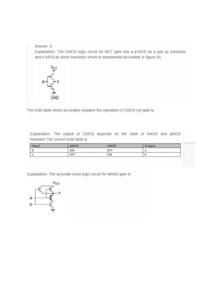
- 7. The CMOS logic circuit for NOR gate is
- 9. 2- input Transistor AND Gate A simple 2-input logic AND gate can be constructed using RTL Resistor- transistor switches connected together as shown below with the inputs connected directly to the transistor bases. Both transistors must be saturated “ON” for an output at Q.