Low Power Clock Distribution Schemes in VLSI Design
•
0 likes•168 views

This paper reviewed the comparison between different clock distribution schemes which used for low power VLSI design which are the most important aspect in the industry. The main clock distribution schemes are single driver clock scheme and distributed buffers clock scheme. There are different tradeoffs in both the techniques such as size of buffers, number of buffers etc.

Recommended
Recommended
More Related Content
What's hot
What's hot (19)
Viewers also liked
Viewers also liked (19)
Similar to Low Power Clock Distribution Schemes in VLSI Design
Similar to Low Power Clock Distribution Schemes in VLSI Design (20)
Recently uploaded
Recently uploaded (20)
Low Power Clock Distribution Schemes in VLSI Design
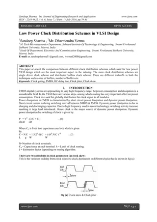
- 1. Sandeep Sharma. Int. Journal of Engineering Research and Application www.ijera.com ISSN : 2248-9622, Vol. 6, Issue 7, ( Part -1) July 2016, pp.79-81 www.ijera.com 79 | P a g e Low Power Clock Distribution Schemes in VLSI Design 1 Sandeep Sharma , 2 Mr. Dharmendra Verma 1 M. Tech-Microelectronics Department, Subharti Institute Of Technology & Engineering, Swami Vivekanand Subharti University, Meerut, India 2 Head Of Department, Electrnics And Comminication Engineering, Swami Vivekanand Subharti University, Meerut, India E-mail: er.sandeepsharma51@gmail.com, vermad2000@gmail.com ABSTRACT This paper reviewed the comparison between different clock distribution schemes which used for low power VLSI design which are the most important aspect in the industry. The main clock distribution schemes are single driver clock scheme and distributed buffers clock scheme. There are different tradeoffs in both the techniques such as size of buffers, number of buffers etc. Keywords: Clock gating, PMBS, RC delay line, Clock jitter, Clock skew. I. INTRODUCTION CMOS digital systems are approaching to very high frequency range. So power consumption and dissipation is a considerable field. In the VLSI there are various steps, among which routing has very important affect on power consumption. Clock tree used for globally distribution the clock signal to all modules. Power dissipation in CMOS is characterized by short circuit power dissipation and dynamic power dissipation. Short circuit current is during switching interval between NMOS & PMOS. Dynamic power dissipation is due to charging and discharging capacitor. Due to high frequency used in recent technology switching activity increase resulting it large load introduced. Hence clock is the major source of dynamic power dissipation. Dynamic power dissipation by switching of clock is given by: P = V2 .f. (C + C ) …(1) clkdd LD Where CL is Total load capacitance on clock which is given by C = N.C + 1.5(2h -1).C + á (4h .N.C )1/4 …(2) L g W W N=Number of clock terminals. Cg = Capacitance at each terminal. h = Level of clock routing. á = Estimation factor depending on routing algorithm. There are two problems in clock generation (a) clock skew: This is the variation in delay from clock source to clock destination in different clocks that is shown in fig (a) Fig (a) Clock skew & Clock jitter RESEARCH ARTICLE OPEN ACCESS
- 2. Sandeep Sharma. Int. Journal of Engineering Research and Application www.ijera.com ISSN : 2248-9622, Vol. 6, Issue 7, ( Part -1) July 2016, pp.79-81 www.ijera.com 80 | P a g e (b) Clock jitter is defined as temporal variation of clock with respect to reference edge. It is of two type long jitter and cycle to cycle jitter. The above both of problems are minimize by using good appropriate clock scheme either single or distributed buffer. Single Buffer: Buffers are used in clock schemes to drive load capacitance and fast tansitions. The single driver scheme has the advantage of avoiding the adjustment of intermediate buffer delay as in distributed buffer schemes. Often in conjuction with this scheme, wire sizing is used to reduce the clock phase delay. Widening the branches that are closed to clock source can also reduce clock source skew caused by asymmetric clock tree load and wire with deviations. If the interconnect resistance of the buffer at the clock source is small as compared to the buffer output resistance, it is called as single driver clock scheme. Distributed buffer scheme: In this, intermediate buffers are inserted in the various part of clock tree. Advantage of using small buffer is flexible to place for save layout. Here clock skew and phase delay is reduced by intermediate buffers. This is the most common and general approach to equi-potential clock distribution scheme. It leads to an asymmetric structure. All paths are balanced in the distributed buffer scheme as shown in fig (b). Fig (b)- Distributed buffer scheme of product of path length and load capacitance. Hence if wire width increase, clock skew decrease but here load capacitance is increase then power dissipation increase. So decrement in power dissipation is done by both path delay and load decreasing. Buffer size can be minimize for reducing power dissipation. It can be formulated as- given a clock tree T, intermediate buffer is inserted by insertion algorithm, the problem of power minimization by buffer sizing(PMBS) is determine buffer size in T, to minimize total power subject to phase delay constraint dp and skew constraint tb s. Clock Gating: It is very useful method for power reduction of clock signals. In this actually we use gating function to turn off the clock feeding the module when there is no clock required for some extended period. Clock gating saves power by reducing unnecessary clock activities in the module. During the process some modules in a processor unit may be left ideal for an extensive period depending upon the software it is executing. Intermediate small buffer and wire widening is used to reduce delay. But wire widening require large size of buffer at source. In single driver short circuit power dissipation is more than distributed buffer scheme due to the reason of small buffer used in distributed buffer scheme. Clock line can also be treated as RC delay lie as shown in fig (c). Fig(c)-Clock line treated as RC delay line Clock skew between source s1 and s2 is given by
- 3. Sandeep Sharma. Int. Journal of Engineering Research and Application www.ijera.com ISSN : 2248-9622, Vol. 6, Issue 7, ( Part -1) July 2016, pp.79-81 www.ijera.com 81 | P a g e ts=RL1.CL1/w1 –RL2.CL2/w2 ...(3) without wire width variation skew is linear function of path length and with wire width variation skew is linear function Fig. (d) Clock Gating The design complexity and clock gating performance degradation are generally manageable. The gated clock signal suffers an additional gate delay due to the gating function. In most high performance chip design, the clock distribution network consists of a multiple hierarchy tree feeding the sequential elements e.g. Tree, H- Tree, X-Tree, Mesh, etc. The masking gate simply replaces one of the buffers in the clock distribution tree. Therefore, the delay penalty is not a concern. II. CONCLUSION Clock delay and skew minimization is an important problem in design and layout of high speed VLSI circuits, Different problems in clock like clock jitter, clock skew is also incorporated when clock is designed. These problems are eliminated by using different clock schemes which have different tradeoffs. According to requirement appropriate technique is used. REFERENCES [1]. T. G. Noll and E. De Man, “Pushing the performance limits due to power dissipation of future ULSI chips,” in Proc. of the ISCAS’92, San Diego, May 1992, pp. 1652-1655. [2]. Y. Jiren and C. Svensson, “High speed CMOS circuit technique,” IEEE J. Solid-state Circuits, vol. 24, pp. 70, Feb. 1989. [3]. M. Afghahi and C. Svensson, “A unified single phase clocking scheme for VLSI systems,” IEEE J. Solid- state Circuits, vol. 25, pp. 225-233, Feb. 1990. [4]. D. W. Dohberpuhl et al., “A 200-MHz 64-h, dual-issue CMOS microprocessor,” IEEE J. Solid-state circuits, vol. 27, pp. 1555-1566, Nov. 1992. [5]. K. Yano et al., “A 3.8-ns CMOS 16 x 16-h multiplier using complementary pass-transistor logic,” IEEE J. Solid-state Circuits, vol. 25, pp. 388-395, Apr. 1990. [6]. M. Suzuki, “A 1.5 nS 32b CMOS ALU in double pass-transistor logic,” in ZSSCC Dig. Tech. Papers, 1993, pp. 90-91. [7]. K. Kikuchi et al., “A single-chip 16-hit 25 nS real-time videohmage signal processing,” IEEE J. Solid- state Circuits, vol. 24, no. 6, pp. 1662-1667, Dec. 1989 [8]. B.Pontikakis and M. Nekili, “A New Area-Power Efficient Split-Output TSPC CMOS Latch for High- speed VLSIApplications,” International Conference of Microelectronics (ICM2001), Morocco, Oct. 29-3 1,2001. [9]. M.Afghahi and J. Yuan, “Double Edge-Triggered D-Flip- Flops for High-speed CMOS Circuits,” IEEE J. Solid-state Circuits, vol. SC-26, no. 8, pp. 1168-1 170, August 1991. BIOGRAPHY OF AUTHORS Sandeep Sharma is pursuing M.Tech Microelectronics from Subharti Institute Of Technology & Engineering, Swami Vivekanand Subharti University, India. His area of interest is low power VLSI Design. Mr. Dharmendra Verma is Head of Department of Electronics and Communication Engineering, Subharti University. He is interested in Microelectronics Design & Technology. He has guided many B.Tech and M.Tech students. He has also published many papers in National and International Journals.