
Recommended
More Related Content
What's hot
What's hot (18)
Viewers also liked
Viewers also liked (14)
Similar to System design and 8051
Similar to System design and 8051 (20)
Recently uploaded
Recently uploaded (20)
System design and 8051
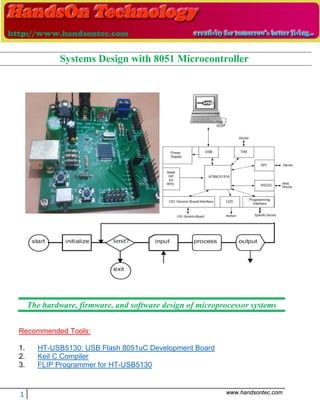
- 1. 1 www.handsontec.com The hardware, firmware, and software design of microprocessor systems Recommended Tools: 1. HT-USB5130: USB Flash 8051uC Development Board 2. Keil C Compiler 3. FLIP Programmer for HT-USB5130 Systems Design with 8051 Microcontroller
- 2. Table of Contents Title Page................................................................................... 1 Table of Contents...................................................................... 5 Section I – Foundations....................................................................4 Section II – Systems.........................................................................6 Section III – Applications...............................................................10 Section IV – Hardware...................................................................11 Section V – Architecture ................................................................12 Section VI – Communication .........................................................13 Section VII – Documentation ........................................................14 SECTION I - FOUNDATIONS 15 1. Introduction ............................................................................ 16 Why this book, now 16 Development environments 18 Book structure 18 Class structure 19 Credit where credit is due 20 2. Fundamental circuits.............................................................. 21 Fundamentals 21 Output 22 Input 23 Computer vs. microcontroller 24 History 101 24 Microcontroller 25 Microcontroller input/output 26 Sink or source 27 Propagation delay and power consumption 28 External input/output 29 3. Memory devices ...................................................................... 31 Where do you keep it 31
- 3. Table of Contents 5 Program 31 Data 32 Dual in-line package 32 Connections 33 How it works 34 Other uses 34 4. Project 0 - Memory.................................................................36 Project 0: Math using ROM 36 5. Micro primer...........................................................................38 Its all in the family 38 On-board data memory 39 Arithmetic 39 Other packages 40 Flash microcontroller 40 Program memory locks 40 Features 41 The extended family 42 6. Address and interface.............................................................43 What is the connection 43 Power 43 Clock 43 Reset 45 Ports 45 Port 0 46 Port 2 46 External memory 47 External program 47 External data 48 External 64K 48 Port 1 49 Port 3 49 7. Minimum system.....................................................................50 Minimalist 50 Project 51 Minimum software 51 Opcodes, mnemonics, comments 52 Classes of instructions 53 Schematic 53 8. Machine cycle time .................................................................55 First computer circuit 55
- 4. 6 Systems Design and the 8051 Durham Cycle time 56 Machine cycles 57 Long precise wait 58 In from out 58 Switch a bit 59 Circuit: led metronome 60 9. Project 1 – Output & time delay ........................................... 61 Project 1: Metronome 61 Program sample example 63 10. Software development............................................................ 66 The here and now 66 Instructions 67 Assembler directives 69 Step by step 71 Program with comments 71 Listing 73 Intel hex 75 Commentary 76 The top placement 77 The subs 78 Your comments, please 78 The bottom placement 79 Structure 79 11. Design practices ...................................................................... 81 Top down 81 Extreme programming (XP) 82 Steps for success 83 Process diagram 85 SECTION II - SYSTEMS 86 12. Switch, logic, and subs............................................................ 87 Switch hitter 87 Debounce 88 Bit manipulation 88 Masking logic 89 Rotate and exchange 90 Conditional branch 91 Subroutines 92 Stack 93 Circuit: led and switch 95
- 5. Table of Contents 7 13. Project 2 – Input & decisions.................................................96 Project 2: T-bird taillights 96 Program sample example 99 14. Register, timers, and interrupts ..........................................103 Timer registers 103 Timer 104 Interrupts 105 Counter & interrupt examples 106 Timer with interrupt examples 107 Circuit: interrupts 108 15. Project 3 – Clock & interrupt..............................................109 Project 3: Time to count 109 Program sample example 111 16. Board construction ...............................................................115 One step. Check! 115 Show and tell 115 Basics 116 Socket to me 117 What’s left 118 17. Project 4 - Development board............................................119 Project 4: Build from scratch 119 18. External memory ..................................................................122 Storage control lines 122 Address fetching 123 Timing sequence 124 Virtual memory 125 Wiring ROM or RAM 126 19. Bios.........................................................................................128 Definition 128 Bios main 129 Static memory test 130 Download 132 Downbyte 134 Checksum 135 ASCII to hex conversion 136 Memory switch 137 Use of low memory 139 20. Project 5 – Bios development tool .......................................140 Project 5: Develop operating system 140
- 6. 8 Systems Design and the 8051 Durham 21. Serial communications......................................................... 144 Background 144 Microcontroller 146 Generating baud rates 146 Mode 0 147 Mode 1 147 Mode 2 148 Mode 3 148 Timer/counter 2 baud rates 148 Timer baud table 149 Timer 1 and color burst 149 Serial initialization 150 Serial data protocol 151 Serial buffer 153 Circuit: serial 154 22. Project 6 – RS232 communications..................................... 155 Project 6: RS 232 to PC exchange 155 Program sample example 158 23. Expansion latches ................................................................. 162 I/O expansion port 162 I/O expansion memory 163 Latch in/out connection 163 Latch in/out code 165 24. Memory-mapped input and output..................................... 167 Accessing external data 167 The instruction 168 The setup 169 The hook-up 169 Latch in/out memory-mapped 171 25. Project 7 – I/O expansion..................................................... 173 Project 7: Unlimited I/O 173 Program sample example 175 26. Tables..................................................................................... 177 Data in code memory 177 Data byte 178 Characters available table 179 Movx vs. movc 181 Code messages 182 Enhanced serial messages 183
- 7. Table of Contents 9 27. Multiplexing ..........................................................................185 Perception 185 Multiplex 186 Circuit: displays 187 Code requirements 189 Code segment for port 190 Code segment for memory map 190 Binary to binary coded decimal 191 28. Project 8 - Seven-segment displays .....................................193 Project 8: Seeing what is not there 193 Program sample example 196 29. Matrix scanning ....................................................................200 Matrix inputs 200 Contact arrangement 201 Conflicts 203 Key debounce 203 Decipher 204 Complete solution 205 Connections 205 Test code 206 Decode flowchart 207 Keys procedure 210 Simple solution 211 Circuit: keypad 214 30. Project 9 - Keypad ................................................................215 Project 9: Debounce & matrix inputs 215 Program sample example 217 31. Liquid crystal display...........................................................226 Different display systems 226 LCD variations 227 Connections 227 Control 228 Control via port 229 Control via latch 230 Control via PLD 231 Command 232 Initialization 233 Cursor position 234 Message display 235 32. Project 10 - Text display ......................................................236
- 8. 10 Systems Design and the 8051 Durham Project 10: Text message screens 236 Program sample example 238 SECTION III - APPLICATIONS 249 33. Infrared communications .................................................... 250 Local wireless 250 Philips protocol 251 Detected string 253 Connections 255 Circuit: infrared receiver 255 34. Project 11 - Wireless............................................................. 256 Project 11: Communicate with IR 256 Program sample example 258 35. Serial chips – IIC .................................................................. 263 Other chip interfaces 263 Inter integrated circuit 264 IIC details 265 IIC sequence 267 IIC bit bang 268 36. Serial chips – SPI.................................................................. 271 Serial peripheral interface 271 Analog to digital sensitivity 272 Analog to digital noise 273 LTC 1098 clocking 274 LTC 1098 operation 274 Program: LTC 1098 bit-bang 275 Onboard SPI control register 279 Program: EEPROM SPI register 280 TLC549 clocking 285 Circuit: SPI 286 37. Project 12 - A to D converter............................................... 287 Project 12: Analog / digital converter 287 Program sample example 289 38. Waveform synthesis.............................................................. 293 Real world output 293 Sensitivity 294 Circuit: digital to analog 295 Software 295 39. Project 13 – D to A converter .............................................. 297
- 9. Table of Contents 11 Project 13: Analog output 297 Program sample example 299 40. Project 14 - Photosensor.......................................................302 Project 14: Barcode reader 302 41. Project 15 – Analog control .................................................304 Project 15: Pulse width modulation 304 42. Project 16 - Digital feedback................................................308 Project 16: DC motor speed control 308 43. Math functions......................................................................311 Arithmetic 311 Extended precision 312 SECTION IV – HARDWARE 327 44. Parts and pin-outs.................................................................328 Watch your money 328 Proto then uC board 329 uC board only 329 uC board optional 330 Projects 330 uC board headers & jumpers 331 PLD / PEEL pin-out 331 Microprocessor pin-out 332 Buffer pin-out 333 RS232 & RS233 pin-out 334 7-Segment & LCD pin-out 335 A/D Converter pin-out 336 Memory pin-out 337 Cable pin-out, SPI & serial 338 45. Development board...............................................................340 Design 340 Options 340 HyperTerminal 341 Test Program 341 Schematic 341 Board specifications 343 46. In system programming .......................................................349 Serial downloading 349 Programming algorithm 350 Programming instruction 351
- 10. 12 Systems Design and the 8051 Durham Programming schematic 352 Peripheral timing 352 Programming and printer 353 Connectors 354 SECTION V – ARCHITECTURE 356 47. Instruction set ....................................................................... 357 Microcontroller instruction set 357 Addressing modes 358 Data transfer 359 Arithmetic operations 360 Program branching 361 Logical operations 362 Bit manipulation 363 Instructions that affect flags 363 Instruction set 364 48. Memory organization........................................................... 366 Harvard vs. Princeton 366 Code addresses 367 External data addresses 368 Data memory expansion 368 Internal data addresses 369 Internal RAM low 371 Internal RAM high 372 Predefined bit addresses 373 Predefined bits port 3 374 49. Special function registers..................................................... 375 Reserved memory 375 Ports 376 Port 0 376 Port 1 377 Port 2 377 Port 3 377 PSW: Program status word 378 PCON: Power control register 379 Interrupts 380 IE: Interrupt enable register 381 IP: Interrupt priority register 381 Timer / counters 382 TCON: Timer/counter control register 383 TMOD: Timer/counter mode register 383
- 11. Table of Contents 13 Serial 385 SCON: Serial control register 385 50. SFR extended ........................................................................387 Enhanced registers 387 Timer/counter 2 387 T2CON: Timer/counter 2 control register 389 T2MOD: Timer 2 mode register 390 Timer 2 data registers 390 Serial peripheral interface 391 SPCR: SPI control register 392 SPSR: SPI status register 393 SPDR: SPI data register 394 WMCON: Watchdog 394 Using onboard EEPROM 395 SECTION VI – COMMUNICATION 399 51. Ascii........................................................................................400 What is it 400 ASCII-hex table 401 52. Rs 232.....................................................................................403 Connections 403 RS 232 pin outs 404 Schematic 405 Development board pin outs 406 53. Network connection..............................................................407 Network 407 Diagram – digital network 409 Diagram – analog telephone 409 Diagram – analog audio 410 54. Programmable logic device..................................................411 It is just logic 411 Combinational logic 412 First time user 413 Gated latch 414 OLMC and pin assigments 414 Registers 415 Combination output enable 416 Limitations 417 Program: combinational logic (*.psf) 417 Created Files 421
- 12. 14 Systems Design and the 8051 Durham 55. Circuit time & phase shift.................................................... 422 Background 422 Delay 423 Clock signals 424 Interaction 424 Ext program memory read cycle 426 Ext data memory read cycle 426 Ext data memory write cycle 427 SECTION VII – DOCUMENTATION 428 56. Extreme programming (XP) harmonization...................... 429 General guidelines 429 Program specifics 430 57. Documentation...................................................................... 442 Report 442 Computer aided design 444 58. End......................................................................................... 446 59. Author.................................................................................... 447 ž Ÿ
- 13. SECTION I - FOUNDATIONS ž Ÿ
- 14. 1 INTRODUCTION Thought Engineering is the tradeoff between quality, time, and money You can have two, but you cannot have all three. MOD Why this book, now ______________ Why is there a need for another book on system design or on the 8051 microcontroller? Actually, the answer is quite simple. There are numerous books on systems and digital design. There are even several on the 8051. However, we have found no reference that treats the 8051 as the basis of a system. In addition, most books present substantial theory before introducing projects. The task of this book is to start building projects immediately after discussion of the relevant topics. After all, that is why most people want to be an engineer – it is to build objects and see them work. Most books and articles on the 8051 treat it as a simple device, suitable for just a few tasks. Most authors have sample projects, but they are not integrated. On the other hand, I have used the microcontroller family as a basis for industrial and commercial systems for over 20 years. I have also used it as the foundation for an upper / graduate level university design class.
- 15. Chapter 1 Introduction 17 Why use the 8051 architecture? The core of the 8051 arguably is used more than any other device. It is an expansion of the i8042 architecture, which is the fundamental processor used in keyboards for personal computers. Phenomenally, the architecture has been around for over 25 years. It is constantly being enhanced by various vendors to perform tremendous tasks. What is meant by a system design with the microcontroller? One microcontroller forms the kernel for all the electronic and digital functions associated with a system. The power of the 8051 devices makes it very capable of filling the functions of a much larger computer system. The system approach is to integrate together in one microprocessor every task simultaneously. These include digital in, digital out, analog in, analog out, serial communications with other computers, keypad, seven-segment display, liquid crystal display, local and remote control, data logging, 32-bit math calculations with square root, and all this in a real time environment. That is a system! An earlier reference, Microcontrollers in Systems Design began the task. It was very project oriented with an inclusive reference for the 8051. However, it had one shortcoming. It required the reader to have a good grasp of computer systems and (s)he had to translate the reference material into the projects. This work, Systems Design and the 8051, takes a different tack. It is based on engineering design principles that are elucidated as required. Extreme programming (XP) approach to compatibility allows each new project to be integrated as a separate, but interactive module. The book begins with the fundamentals and sequentially adds new projects. This is accomplished by integrating a straightforward and concise application explanation for all software commands. That is followed by a circuit representation of the new components. The project requirements are laid out. Finally, an exemplar program shows a similar system that the designer can modify to complete the project.
- 16. 18 Systems Design and the 8051 Durham The procedure can obviously work. For many years, I have had students step-by-step build a functioning, integrated computer system around 10 projects. They start with a parts list, obtain the parts, and build the projects into a working system. This is done in a single semester. What an accomplishment! Development environments ________ In most design environments, hardware and software are segmented. Moreover, specialists typically handle the tasks separately. While this may be beneficial for large systems development, it restricts understanding of the overall big picture of computer applications. This treatise will present the application of both hardware and software to the solution of real problems. The most effective piece of equipment to provide a simultaneous understanding of computer architecture and programming is the microcontroller. The microcontroller has a complete computer built on a chip. In addition, much of the interface hardware to outside components has been included on the chip. A working computer is obtained by connecting switches to the input, digital displays to the output, and adding a program to the memory. The prerequisites for being able to successfully build the projects are minimal. A reasonable understanding of TTL digital logic is assumed. Proficiency in a high level programming language is also assumed. Understanding of an assembly language would be very beneficial, but is not necessary. Book structure __________________ The structure of the treatise is to provide a working tool that can be readily referenced. The first topics are general items and fundamental connections. The next area is a group of projects that can be constructed. Chapters that give the foundation material precede each project. An exemplar program that can be modified to complete the project follows the project description.
- 17. Chapter 1 Introduction 19 A parts list and development board are discussed. The instructions and memory organization comes next. This is followed by communications protocols. Then, a programmable logic device (PLD) representation is used for the combinational logic. The final chapters are documentation techniques. It is a good idea to look over these section to have an idea of the available reference material for use as the projects are developed. The projects will begin with using a memory device as a table for arithmetic functions. A number of projects will be constructed for performing common control tasks. The epitome of control will entail communications between two computers. The projects are for demonstration of technology and gaining of experience. Where necessary, a schematic and/or software are provided. Often this is an illustration of a related idea. It is not intended to be a solution to the project. It is intended to provide a framework for tackling the project. Class structure __________________ It is not necessary to perform all the projects or to do them all in order to obtain a working knowledge of microprocessors. A proven procedure is to use Project 1, 2, and 3. Project 4 can be included if a development board is used. Then Project 6 and 7 should be completed. These will provide the foundation to do any project. The remaining projects can be used in almost any order, if desired. Projects 8, 9, and 10 provide human interface devices. Project 11, 12 and 13 give infrared communications and analog / digital conversion exposure. Within a semester, I typically use 1, 2, 3, 4, 6, 7, 8, 9, 10 and a choice of 11, 12, or 13.
- 18. 20 Systems Design and the 8051 Durham You can accomplish the tasks. The projects should prove both challenging and enjoyable. Occasionally, you may be frustrated but persevere. As a result, the completion of the task will be most rewarding. The material comes with a guarantee. If you complete all the tasks, you will have the tools to design a computer system for any purpose. Good Computing! Credit where credit is due _________ Everything we know is developed from something we have read, heard, or seen. Therefore, these other thoughts necessarily influence what we write. To the best of our knowledge, we have given specific credit where appropriate. Rather than footnotes or references, we have listed the works that have provided significant information in one way or another, since this is often in concepts rather than quotes. Some of the information is general and public domain, while some is device specific. The generic information is used where possible. Statements that are attributed to us are things we have used commonly and do not recall seeing from someone else. Others obviously have similar thoughts. If we have made an oversight in any credits, we apologize and we would appreciate your comments. Dr. Marcus O. Durham ž Ÿ
- 19. 2 FUNDAMENTAL CIRCUITS Thought Tell me the input, output, and what to do in between, then I can write a computer program. Capt. Ed Fischel, USAF Fundamentals ___________________ What are the fundamentals? Is it not input, output, and how these are related? A mechanical switch represents every type of input there is in a digital world. Similarly, a lamp or light emitting diode (LED) is a surrogate for every possible output. These two simple devices can effectively interface to any real world circumstance by placing a buffer between the digital components and the external items. Hence, a transistor or gate can substitute for the switch and LED. The power for most digital computer devices historically has been 5 volts DC referenced to ground. In many of the newer technologies, this level is dropping below 2 volts. Regardless, the power voltage is called VCC and has a digital value of 1 or True. Similarly, the reference ground is zero volts, is called VSS, and has a digital value of 0 or False.
- 20. 22 Systems Design and the 8051 Durham The power is connected to the upper right corner of most chips. Similarly, the ground is connected to the lower left corner. Output _________________________ Since a light emitting diode (LED) is a logic device, it has polarity. The positive connection is called the anode, it is the longest lead, and is the arrow side of the diagram. The negative terminal is the cathode, it has a flat spot on the edge of the LED, and is the bar in the diagram. A diode has a very low internal resistance. Hence, it has very limited current handling capability. If it were connected directly from power to ground, the current through the low resistance would rise very high. The power dissipation would increase by the square of the current. Then the diode would burn out or blow. To restrict the current, common practice is to place a resistor in series with the LED. In restricting the current, the brightness is reduced. Therefore, for optimum brightness, the series resistor should be calculated to give the optimum current. VCC Ground Various light emitting diodes have a voltage drop of 1.4 to 2.5 Volts. The maximum current for different LEDs is 20 up to 750 mA. However, the current must be restricted below the maximum that can be supplied by the gate. To limit the current a resistor is placed in series. Assume a current of 5 mA and 1.5 V drop. R = V / I = 1.5 V/ 5 mA = 300 : Typical values are 270 to 330 Ohms. If the lamp is not bright enough, the specifics should be verified, and a different resistor should be calculated.
- 21. Chapter 2 Fundamental Circuits 23 Input ___________________________ A switch must represent two states, both off and on. Therefore, it must be connected to both power and ground. To prevent a short circuit when the switch is closed, a resistor is placed between the power and the switch. This is called a pull-up resistor. The other side of the switch is connected to ground. The output of the switch is taken between the resistor and the switch. The other side of the output is ground. VCC Out Ground The resistor must be sized to limit the current in a short-circuit condition. Many devices have a 10 mA limit on the amount of current they can sink. When connecting a switch as a short circuit, the current is often limited to 2.5 mA. Therefore, the resistor is sized based on that value. For a voltage source of 5 V and a current load of 2.5 mA, the resistance is calculated from Georg Ohm’s rather famous law. R = V / I = 5 V / 2.5 mA = 2000 Ohm The common sized pull-up resistor is typically 2,000 to 2,200 Ohms. Next consider the power rating of the resistor. P = V*V / R = 5*5 / 2200 = 0.011 W At this low quantity of power, virtually any resistor network has adequate dissipation capability.
- 22. 24 Systems Design and the 8051 Durham Computer vs. microcontroller ______ What is the difference in a computer, microprocessor, and microcontroller? A computer is a device with an internal processor, memory, and interface for input and output. The processor consists of a central processing unit, a control unit, and an arithmetic processing unit. A computer is a complete system, while a microprocessor is basically the core of the unit. The microprocessor will generally require other chips to connect to the input / output interface. A microcontroller is a microprocessor with additional interface components as part of the chip. In essence, a microcontroller is designed to connect directly to the input and output. In addition, it has some memory as part of the chip. In some cases, these are also called single chip computers. A microcomputer is typically designed for general-purpose applications. A microcontroller usually has a dedicated purpose as a control or instrumentation device. History 101 _____________________ The computer was originally developed during World War II. These machines were physically very large, but had limited memory. Large computers continued to develop until the very powerful mainframe systems of the 1960’s. These machines still had discrete magnetic core memory, transistors, and diodes. At that time, the first integrated circuits (ICs) were being developed. From the earliest days of the IC, microcomputers have been a major component. A brief chronology of the microcomputer shows the rapidity of the development. 1968 Intel formed from Fairchild Semiconductor
- 23. Chapter 2 Fundamental Circuits 25 1971 Intel 4004 – 4 bit calculator 1972 Intel 8008 – eight bit 1974 Intel 8080 – eight bit TTL compatible Motorola 6800 MOS Technology 6502 1978 Intel 8086 – sixteen bit basis of PC 1979 Intel 8051 – eight bit microcontroller It is fascinating that the architecture and software of the 8051 has continued for over 20 years. It is the core architecture for over half of all microcontrollers. Microcontroller _________________ The basic computer circuit is actually very simple. First power and ground are connected to the upper right and lower left pins respectively. Next, a crystal is connected to the XTAL pins to provide stimulus for the internal oscillator. An 11.059 MHz crystal will provide good performance and excellent communications. Other choices are available and can be found in later sections. A very small coupling capacitor of 10 – 40 pf is connected from each side of the crystal to ground. Third, pulling the RESET line high restarts the processor. The RESET line can float low during normal operation. A power-on reset circuit is often connected to the pin to automatically perform the start function. When using a flash microcontroller, a method of loading the program is required. Program loading involves three lines, an input for instructions, an output for data, and an input for clocking the other two lines. An illustration is given in the figure below. Details for implementing the in-system feature are provided in a chapter on in-system programming in the reference section after the projects. For microcontrollers without in-system programming, these lines are not required.
- 24. 26 Systems Design and the 8051 Durham Microcontroller input/output ______ The input / output interface is the defining feature of a microcontroller. On the processor, there are four different ports for this function. Each port represents one byte, which is connected in parallel to pins of the chip. The port is identified as a special function register within the internal RAM. Because of the address of the ports, all are bit addressable. The ports are bi-directional. In default operation, the port will output a byte or bits of data. Any bit of the port can be converted to input. Simply send a one to the bit of the port. Then that bit can be read or input. If all ones are sent to a port, then the entire byte becomes an input. The internal circuitry for one bit of a port is shown. A latch holds the output to the pin. A separate line provides the input. For output, data is written to the port. The result is displayed on the pin. For input, a one is sent to the port. This enables the line and VCC P1.5 MOSI P1.6 MISO P1.7 SCK Reset Xtal2 Xtal1 Ground P1.5 MOSI P1.6 MISO P1.7 SCK Reset
- 25. Chapter 2 Fundamental Circuits 27 pulls the pin high. Therefore, with no other connection to the pin, input from the port bit will be one. If the pin is pulled low by an external switch, then the input is a zero. VCC port in Sink or source ___________________ Connecting external devices to a gate can critically impact the chip. A gate, whether in a microcontroller or a logic device, is limited to the amount of current it can handle. If too much current is drawn by an external connection, the chip may be damaged. Therefore, a resistor or a buffer must limit the current. A chip may provide VCC or Ground to the external devices. Supplying VCC is the high state and is a source for current. Supplying the ground connection is the low state and is a sink for current. Sink current is the amount of current that will flow into an output, IOL, at low state. Source current is the amount of current that will flow out of a gate, IOH, at the high state. Total source (IOH) = input to load (IIH) * number of loads (m) Total sink (IOL) = input to load (IIL) * number of loads (n) The number of loads is called fan-out. The limiting fan-out is the lower of the number of loads (m or n). The maximum current, and resulting fan-out, must be observed to preclude overloading and damaging a gate. When interfacing to different logic families, total the load current for all devices. Q Latch Q’ pin
- 26. 28 Systems Design and the 8051 Durham Propagation delay and power consumption Two other parameters determine the performance of a gate. Propagation delay is the delay of low-to-high (tPLH)and high-to-low (tPHL) transitions between the input and output of a gate. tPLH tPHL For TTL logic, power consumption is an average of power consumption for high and low state output. PD = VCC * (ICCH + ICCL) /2 The table below gives the performance for various logic families. A minus sign indicates current is flowing out of the gate. A later chapter on circuit time and phase shift addresses the timing and propagation delay in more detail. Description Range Unit Sym S LS AS ALS F CMOS Propagation delay typical Ns tPD 3 9 1.7 4 3 P consumption per gate avg. mW PD 19 2 8 1.2 4 Speed*power (energy) pJ E 57 18 13.6 4.8 12 Low-level input voltage max V VIL 0.8 0.8 0.8 0.8 0.8 1.5 Low level output voltage max V VOL 0.5 0.5 0.5 0.5 0.5 0.05 High-level input voltage max V VIH 2.0 2.0 2.0 2.0 2.0 3.5 High-level output voltagemax V VOH 2.7 2.7 2.7 2.7 2.7 4.95 Low-level input current max mA IIL -2.0 -0.4 -0.5 -0.2 -0.6 -0.1 PA Low-level output current max mA IIH 20 20 20 8 20 0.1 PA High-level input current max mA IOL 50 8 20 20 20 0.88 PA High-level output current max PA IOH 1000 -400 -2000 -400 -1000 -0.88 PA
- 27. Chapter 2 Fundamental Circuits 29 External input/output _____________ An LED is shown connected with the chip as a sink. In this mode, a zero “0” is sent to the port to illuminate the LED. This is the preferred approach since chips sink more current than they can source. Vcc port This circuit is very similar to that used for a switch input. Vcc port ground In this schematic, an LED is shown connected with the chip as a source. In this mode a one “1” is sent to the pin to illuminate the LED. This is a poor design since the chip is limited in the amount of current it can source. Port Ground One circuit of particular interest combines both an LED and a switch on a single port pin. This permits both a display and an input. Vcc port
- 28. 30 Systems Design and the 8051 Durham When the switch is closed, the lamp will be on. Therefore, the switch must be open for the lamp to be controlled by the port. When the port sends a zero, the lamp is on. When the port sends a one, the lamp is off, and the switch can be read. ž Ÿ
- 29. 3 MEMORY DEVICES Thought Memory is the second thing to go. He just does not remember the first. Old quip Where do you keep it _____________ Two fundamental types of memory are typically used in a computer system. These are program memory and data memory. Program memory is static and seldom changes. Data memory is dynamic and changes with the conditions. These functions determine the technology that can be used for each purpose. Program ________________________ Program memory is typically completely changed when there is a new program. Program memory can use one time technology. This includes devices such as read only memory (ROM). The basic version is programmable ROM or PROM. Enhanced versions allow the device to be erased by ultraviolet light and programmed by special hardware. These are called erasable programmable ROM or EPROM. As technology advanced, the chip could be erased and programmed by changing the voltage. These are electrically erased PROM or
- 30. 32 Systems Design and the 8051 Durham EEPROM. A variation of the technology is called flash memory. The erasure and programming capability is built into the chip. This is selected by using one of the pins. Data ___________________________ Data memory requires the status to be changed frequently. Only a part of the memory is typically involved. Therefore, random access memory (RAM) is used. Not surprisingly, this technology is more complex. Some internal memory uses EEPROM technology to accomplish this purpose. Because of the technology, the number of read/ write cycles is often limited. Dual in-line package _____________ A common version of separate memory chips uses dual inline packaging (DIP). These are typically limited to prototyping or limited quantity projects. The quantity of memory in the package is constantly increasing as technology improves. To handle the additional pins, other package technologies are often used for production devices. The pin-out for static RAM, PROM, and EEPROM is almost identical. There are two basic differences. The programming pins are called write pins and the output enable pins are called the read pins. A typical 32K address X 8-bit byte package is illustrated as a 256K bit device in the following diagram.
- 31. Chapter 3 Memory Devices 33 Connections _____________________ Like most other DIP packages, power is supplied to the upper right (pin 28), and ground is supplied to the lower left (pin14). * V A14 1 28 VCC A12 2 27 /WE A7 3 26 A13 A6 4 25 A8 A5 5 24 A9 A4 6 23 A11 A3 7 22 //OE A2 8 21 A10 A1 9 20 //CE A0 10 19 DQ7 DQ0 11 18 DQ6 DQ1 12 17 DQ5 DQ2 13 16 DQ4 Ground 14 15 DQ3 Memory 256K In addition, the chip must be selected or enabled. The Chip Enable not (/CE) line must be pulled low for the chip to function. If there are multiple memory chips, this is done by an address decoding chip. If there is only one chip, then the line is simply connected low. There is one precaution about connecting address lines on the memory chip. Avoid letting any pin float. Connect the line to an address decoder. If the address line is unused, connect it to ground. When sending data to the chip, the Write Enable not (/WE) line must be pulled low. When obtaining data from the chip, the Output Enable not (/OE) line must be pulled low. Obviously, the two lines should not be pulled low simultaneously.
- 32. 34 Systems Design and the 8051 Durham How it works ____________________ Since reading is common to both types of memory, an output or read will be used as a description of how a memory chip works. The combination of address lines is used to select a particular byte of information stored in the memory. The information stored in that location will be imposed on the output pins. The number of addresses is a power of two function of the address lines. If there are ‘m’ address lines, then the number of addresses can be calculated easily. Addresses = 2m For eight (8) address connections, there are 256 addresses. The first address is zero (0) and the last would be 255. Ten addresses lines would access 1024 locations. In common usage, this is rounded down and called a 1K device. Larger sizes are proportionally rounded to give common sizes that are powers of two. A few examples are 16K, 32K, 64K, and 512K. Each address accesses ‘n’ bits of information stored in the memory and displayed on the output. In microcontroller systems, the number of bits is 8 and is called a byte. The total number of bits is used to describe memory devices. The number of addresses and the number of bits output determines the size of the memory. For example, a chip with 8 address lines and 8 output lines would be a 2K device. 2m * 8 = 28 * 8 = 2048 Other uses ______________________ Since the chip will have an output based on the status of the address lines, it can be used to represent a conventional logic network. There are ‘n’ outputs and each output can have 2m maxterms.
- 33. Chapter 3 Memory Devices 35 The ROM has fixed values, which makes it well suited for projects that require a table lookup. This is particularly appropriate for mathematics problems that are repeated frequently. Consider an example. Given: y = 2 x2 – 1 Allowable range: 0 d x d 3 What is the address (input) variable? x What is the data (output) variable? y How many addresses are there? 4 (0, 1, 2, 3) How many address lines are required? m = 2 o 2m = 4 What is the largest value output? 17 How many output lines are required? n = 5 o 2n = 32 Create a table of values to implement the function. Negative values are represented by setting the most significant bit (MSB) to 1. Decimal numbers can also be represented by setting another bit. Input Address lines Memory Output lines 0 00 -1 100001 1 01 1 00001 2 10 7 00111 3 11 17 10001 By connecting switches to the address lines and LED’s to the output lines, the special purpose calculator is realized. ž Ÿ
- 34. 4 PROJECT 0 - MEMORY Thought Skip this project, if not using external memory. Project 0: Math using ROM _______ Purpose: Skip this project if you are not using external memory. To show the function of a ROM. To program an EPROM. Preamble: Every microcomputer has a Read Only Memory (ROM) to store the basic system program. In the case of a development system, a programmable and erasable ROM is preferred. Erasable Programmable Read Only Memory (EPROM) is the most common example. EPROM has lower cost than most other alternatives. An EPROM contains fuses. These are disconnected or left as is to create a pattern of information called programs. An EPROM has address lines usually called A1, A2...An, on the circuit diagram. The EPROM data lines are accessed for the output. The lines usually are called O1, O2, O3...On. The function of address and data lines is exactly the same as the ones on a ROM. Placing information in an EPROM is called
- 35. Chapter 4 Project 0 - Memory 37 programming. Exposing the EPROM to an ultraviolet (UV) light source will clear all locations of their programmed contents. The duration of the exposure depends on the UV intensity. An alternative is electrically erasable memory (EEPROM). The programmer / burner electrically erases this version of storage. The EEPROM is much faster and easier to erase and program. Plan: Demonstrate a ROM is a program memory. Program the ROM to act as a table for a certain function. Preparation: Prepare a breadboard with a +5V power supply. Observe the EPROM data sheet. Then wire light emitting diodes on the EPROM data lines. Wire five switches on the address lines. Investigate the use of the EPROM burner program on the personal computer (PC). Become very familiar with these tools since they will be used in burning all programmable chips. Before burning an EPROM, make sure that the device is blank. Check the EPROM to ensure any lock bits are off. Procedure: Implement the function F = x3 on the EPROM. Use the address lines as the inputs (x) and data line as the outputs(F). Only 5 switches are required on the address lines. Presentation: Demonstrate the output for x = 0, 1, 2...5. Only selected numbers will be requested for demonstration. ž Ÿ
- 36. 5 MICRO PRIMER Thought Prim and proper is an old Southern saying for ‘You have got it together.’ Its all in the family _______________ The 8051 family is the dominant core among all microcontrollers. Intel originally developed the architecture about 1979. Other vendors took the basic device and developed enhanced versions. Various reports are that versions of the device represent over half of all microcontrollers. The standard package is a 40-pin, dual-in-line package (DIP) with 600-mil spacing between the rows of pins. It is without program memory and has only 128 bytes of data memory. Program and data memory are external chips. The most popular variation has program memory and data memory on board the processor chip. In this family of computers, program memory is separate from data. This is called Harvard architecture and it is the design used by Intel related machines. Mixed memory is Von Neumann’s Princeton architecture. It is the design used by Motorola related machines. Reduced instruction set computers (RISC) have very few instructions but these can access any register in the computer.
- 37. Chapter 5 Micro Primer 39 Complex instruction set computers (CISC) have many instructions and each is used to access a limited register or memory. The 8051 has characteristics of both because of its memory and software strategy. However, it is primarily a CISC device. On-board data memory ___________ The on-board data memory is divided into three memory areas. First, there are 128 bytes of general purpose RAM. A significant portion of this can also be accessed as registers or as bits. The next 128 bytes are segmented into 21 Special Function Registers (SFR). These bytes are the only ones accessible from the upper 128 locations on a standard machine. The twenty-one memory locations accessed as special registers cover many areas. A & B accumulators Timer/counter mode and control Serial port mode and control Stack pointer Data pointer Program status word for flags Interrupt enable and priority Parallel ports 0, 1, 2, and 3 for data I/O Many machines now make an additional 128 bytes available as an extended internal RAM. Additional data memory is often available in the form of EEPROM or similar technology. Arithmetic ______________________ Arithmetic functions are unsigned, binary integers. Familiar commands include add, add with carry, subtract, and subtract with borrow.
- 38. 40 Systems Design and the 8051 Durham There are hardware multiply and divide instructions. The A register is operated on by the B register. The results are in A with B as supplemental. Logical operations include AND, OR, and EXCLUSIVE OR. These operate on A with the results placed back into A. Other packages __________________ In addition to the 40-pin wide DIP package, there are other variations. Although there are surface mount designs, our discussion is oriented to packages that can be used for construction of a small number of units. The programmable logic chip carrier (PLCC) is a square configuration that can fit in some spaces more effectively. Projects that do not require external memory and that can be implemented with only two ports use a very cost and size effective arrangement. This is a 20-pin slim package. Flash microcontroller ____________ One of the variations of the 8051 which has almost everything but the kitchen sink is an Atmel design. Other than part of this section, the section on in-system programming, and the chapter on extended special function registers, all the remaining information in this book is generic and applicable to the entire family of microcontrollers. Atmel’s AT89S8252 flash microcontroller has several significant characteristics. The features are listed in the following table. The standard or core features are shown in the last column of the table. Program memory locks ___________
- 39. Chapter 5 Micro Primer 41 Some versions have three lock bits that can be left unprogrammed (U) or can be programmed (P) to obtain security and prevent further programming or fetching of the program. In prototyping, these are left unprogrammed. The lock bits may be inadvertently set if the burner program is improperly configured. With some in-system programmers, the bits may also be inadvertently set. Once programmed, the lock bits can only be unprogrammed with the Chip Erase operation in either the parallel or serial modes. Alternately, the chip can be placed in a burner and the bits cleared. Features ________________________ MCS51 Compatibility 89s8252 8051 Bytes of in-system memory 8k none Reprogrammable downloadable flash SPI serial interface for program downloading Endurance: 1,000 write/erase cycles Bytes EEPROM 2K none Endurance: 100,000 write/erase cycles Operating range: volts 4 - 6 4.9-5.1 Fully static operation frequency: MHz 0 - 24 3-50 Three-level program memory lock yes Eight bit internal RAM: bytes 256 128 Programmable I/O lines 32 32 Sixteen bit timer/counters 3 2 Interrupt source addresses 6 5 Programmable UART serial channel yes yes SPI serial interface yes none Low-power idle and power-down modes yes none Interrupt recovery from power-down yes none Programmable watchdog timer yes none Data pointer two one Power-off flag yes none
- 40. 42 Systems Design and the 8051 Durham The extended family ______________ The data sheet for the device provides very substantial design information. Much of this is similar to generic controllers. A primer provides all the details about how to use the features that are special to this machine. Both these data sheets are available from the manufacturers and on the web. The diagram illustrates the majors features of the machine. ADDRESS ž Ÿ SERIAL PORT INTERRURT CONTROL 4K ROM 4K ROM BUS CONTROL 4 I/0 PORTS CPU OSC EXTERNAL INTERRUPTS RD WR TIMER 0 128 RAM 128 RAM TIMER 2 TIMER 1 P0 P2 P1 P3 TXD RXD
- 41. 6 ADDRESS AND INTERFACE Thought Education: Learn - Do -Teach What is the connection ____________ The standard 40-pin package is used for most discussions. It contains all the external connections that will be used on any variation of the microcontroller. Some designs do not need all the features. These will be smaller and will not include some pins. Power __________________________ Before anything can work, power must be applied. The upper right (pin 40) is connected to VCC, which is usually 5 volts. The lower left (pin 20) is connected to the ground reference. Clock __________________________ The clock or crystal is connected to pins 18 (XTAL2) and 19 (XTAL1). This provides a frequency basis for all the micro operations and timing. Each cycle is divided into 12 phases which trigger internal circuits to create an instruction.
- 42. 44 Systems Design and the 8051 Durham * V P1.0 1 T2 40 VCC P1.1 2 T2 EX AD0 39 P0.0 P1.2 3 AD1 38 P0.1 P1.3 4 AD2 37 P0.2 P1.4 5 SS/ AD3 36 P0.3 P1.5 6 MOSI AD4 35 P0.4 P1.6 7 MISO AD5 34 P0.5 P1.7 8 SCK AD6 33 P0.6 Reset 9 AD7 32 P0.7 P3.0 10 RXD VPP 31 /EA P3.1 11 TXD PROG/ 30 ALE P3.2 12 INT0 29 /PSEN P3.3 13 INT1 A15 28 P2.7 P3.4 14 T0 A14 27 P2.6 P3.5 15 T1 A13 26 P2.5 P3.6 16 /WR A12 25 P2.4 P3.7 17 /RD A11 24 P2.3 Xtal2 18 A10 23 P2.2 Xtal1 19 A9 22 P2.1 Ground 20 A8 21 P2.0 MCS 51 / 8051 When using a crystal, a buffering capacitor of 10 to 40 pf is connected from each pin to ground. The crystal frequency ranges from 3 to over 50 MHz. However, the choice of frequency is often determined by outside connections. For example, serial communications requires rather unusual frequencies such as 11.059 MHz. If an oscillator is used, XTAL1 is the input to the oscillator amplifier and the input to the internal clock. XTAL2 is the output from the inverting oscillator amplifier.
- 43. Chapter 6 Address & Interface 45 Reset ___________________________ Reset is connected to pin 9. The machine runs when the line is low. Reset occurs if the pin is pulled high for two machine cycles. In the simplest realization, a switch performs this function. The switch should be open for normal operations and momentarily closed for reset. The most elegant circuit occurs with power on. This circuit will automatically reset the computer whenever power is applied. The circuit consists of a 10 microfarad capacitor connected to Vcc and a 10 K Ohm resistor connected to ground. When using in-system programming, the pin may be activated by a software command. A 1500 Ohm resistor should be connected between the cable and the reset pin. Ports ___________________________ Ports are parallel locations within the processor. Each port includes eight bits that are individually addressable. Three different notations are used to represent a bit on a port, as shown in the diagram. These include pin number, port number followed by the bit number, and function such as address / data. Limit the number of devices and resulting current connected to any port. The ability to sink or source current is very restricted. A buffer such as a latch or 7406 is highly desirable to protect the port. Current limiting resistors should be used for LEDs connected directly to the port. The maximum output currents that the chip can handle are shown in the table.
- 44. 46 Systems Design and the 8051 Durham Condition IOL Max per port pin 10 mA Max for eight bit, port 0 26 mA Max for eight bit, port 1,2,3 15 mA Max total for all output pins 71 mA To determine the number of devices that can be connected, it is necessary to identify the current required by each load. Total source (IOH) = input to load (IIH) * number loads (m) Total sink (IOL) = input from load (IIL) * number loads (n) Use lower power devices such as ALS or CMOS technology. Port 0 __________________________ Port 0 consists of eight pins (pins 32-39). As a true bi-directional I/O port, it can be used for normal input and output. As an output, it can sink eight TTL loads. When 1s are written to the pins, they become high-impedance inputs. Therefore, it requires a pull-up or pull-down resistor to operate. Because of other features, it is probably the least used port in normal programming. However, when used as a memory connection, the port has internal pull-up resistors. Port 2 __________________________ Port 2 is another 8-pin I/O connection (pins 21-28). It is less frequently used in normal programming. It is quasi bi-directional, has internal pull-ups, and can sink/source four TTL devices. When 1s are written to the pins, they are pulled high by the internal pull-ups and the pin can be used as an input. As inputs, pins that are externally being pulled low will source current because of the internal pull-ups.
- 45. Chapter 6 Address & Interface 47 External memory ________________ If external data or program is required, then port 0 takes on a multiplexing task. It has eight bits of the address impressed on the port. Then this is followed by the eight bits of data associated with that address. A latch is used to trap the address. An eight bit flip/flop such as a 74573 is commonly used. It contains the 8 bus latches connected to the Data (D) or input pins of the latch. The output or Q pins are connected to the low order address pins of the memory device. Two pins control the data capture and transfer. The chip or latch enable (pin 11) is asserted high, the gates receive and pass information. When the pin is asserted low, the flip/flops trap and hold the information. The output enable not (pin 10) is hardwired low to permanently activate the output. When the 8 address bits are on the port, the Address Latch Enable line (pin 30) is toggled. This pin is connected to the chip enable pin of the external latch. Therefore, when the address is superimposed, the latch will capture and hold the location. External program ________________ If external program memory is employed with the microprocessor, then the External Address (pin 31) must be pulled low. This will transfer all program code from external memory. If there is both internal and external program memory, the internal memory will be accessed when the /EA line is high or not connected. The next address after the top of the internal memory, will go to the external, regardless of the status of /EA.
- 46. 48 Systems Design and the 8051 Durham When a code byte is requested from the program memory, the program storage enable not (/PSEN) is pulled low by the processor. The code will enter on port 0 pins. The /PSEN line is connected to the external programmable read only memory (PROM) device output enable not (/OE) pin 22. The PROM chip select not (/CS) is connected to ground, if it is the only device. If there are multiple devices, the chip select must be decoded perhaps through a programmable logic device (PLD). Do not allow input address pins on any memory device to float. Pull the pin low if it is not connected to the processor. External data ___________________ External data memory is in the form of static ram (SRAM), electrically erasable prom (EEPROM) or similar devices. If these are in a DIP package the pins will correspond with those of program memory. However, the connections to the processor are very different. Data is transferred from the processor to memory when the write not (/WR) pin 16 is pulled low by the processor. The pin is connected to the write enable not (/WE) pin 27 on the memory device. Data is read from external memory when the read not (/RD) pin 17 is pulled asserted low by the processor. This is connected to the read not (/RD) or output enable not (/OE) pin 22 on the memory device. External 64K ____________________ The eight bits on port 0 can address a maximum of 256 bytes of memory. Address = 28 – 1 = 255
- 47. Chapter 6 Address & Interface 49 By using port 2 as the upper eight bits of an address, 64K of external memory can be accessed. Address = 216 – 1 = 65,535 Port 2 is not multiplexed. Therefore, an address latch is not required. The lines of port 2 are wired directly to the corresponding high bit address lines of the memory device. Since the port is bit accessible, any bits not used for addressing are available for use as general purpose I/O. Often the upper bit (A15) is used to select memory or memory-mapped input/output. Port 1 __________________________ Port 1 is the most used general purpose I/O (pins 1-8) on the processor. The internal pull-ups operate like port 2. Most devices are connected through these pins. If the processor has a serial peripheral interface (SPI), it is connected to the upper bits of port 1 (pins 5-8). These pins are connected to external chips. If the SPI is used for in-system programming, these pins are connected to an external cable. Port 3 __________________________ Port 3 is truly a multifunction byte (pins 11-17). The internal pull- ups operate like port 2. Pins not used for other functions can be used for general purpose I/O. The pins provide input for timers and interrupts as well as a bi-directional serial UART. Two pins are shared with the read not and write not functions for external data memory. ž Ÿ
- 48. 7 MINIMUM SYSTEM Thought Elegantly simple Minimalist ______________________ The minimum system for a computer is the ability to do input, decisions, and output based on the decision. This will provide an outline for every other project that can be built. Although the software code is very simple for this type project, the implementation will be in a structure that can support very complex problems. As systems grow, more interaction is needed. A later software illustration identifies issues of compatibility, particularly for variable descriptions. The hardware required covers several issues. First, appropriate power must be supplied to ensure operation in range. Second, the fundamental computer is wired. This includes the processor, crystal, and reset circuit. Third, a method of transferring the code to memory is required. In this implementation, in-system programming is used. Finally, connections to the external world are made in the form of switches for inputs and lamps for outputs. When building a circuit for digital processing, several practices will provide results that are more consistent. Lay out the components adjacent to other components that will be interconnected. Use short
- 49. Chapter 7 Minimum System 51 wires. Red should be used for power. Black is preferred for ground. A variety of other colors for inter-connections will help construction. Keep the board neat, since this will aid troubleshooting and improve your attitude about the project. Project _________________________ The project is to apply one switch and two LED’s to the computer. One LED is on while the other is off. Change the state of the switch and the LEDs will change state. Minimum software _______________ On reset, program control transfers to address 0000h. The number of digits in the address is based on the maximum amount of memory that is directly accessible. There are sixteen bits for addressing. A hexadecimal number is made up of four bits. Sixteen bits then would be divided into four hexadecimal numbers. Addresses 0000 – 0002h are the power on reset vector and are reserved to send the program to another location. Addresses 0003 – 002Ah are reserved for interrupt processing in a standard processor. Many enhanced processors reserve the next 8 bytes for expansion interrupts. Additional explanation is given in the architecture section covering memory organization. Therefore, the lowest code address should be 0033h. However, programmer information and ownership is often embedded in the next code addresses. For that reason, the first address used for program code is usually 0080h. For normal procedures, the first command at address 0000h is a jump to address 0080h. Several jumps are available. These include absolute short, absolute long, and relative. Any of these can be used for the first command in the computer.
- 50. 52 Systems Design and the 8051 Durham Opcodes, mnemonics, comments ___ The most basic level of programming is using machine language and op codes. This can be done for relatively small routines and for practice in debugging. However, it is not time effective for any program of significance. A later chapter introduces higher level language techniques. The opcode list is provided in the reference chapter on instructions set. When coding, it is very desirable to use precise spacing for the instructions. This makes the program easier to read and keeps all the information about each instruction on one line of a standard size paper. The comments will be truncated on the narrow paper of this book. ;add OPCODES LABEL: MNEM REGISTER ;COM 0000 020080 ljmp INITIAL ;go 0080 D2B5 INITIAL: setb 0B5h ;on This is the complete program necessary to turn on an LED connected to port 3, bit number 5. The address is a hexadecimal value from 0000 – FFFFh. Each program location represents an eight bit byte of data. The op codes are hexadecimal values that are decoded and processed by the internal central processing unit. A series of micro operations are executed to create the correct response. Mnemonics are used for convenience in recognizing the instruction. The processor only understands the op codes. In general, an instruction gets data from a source register, operates on the data, and places the results at a destination register. By convention on this particular machine, the destination is noted first. A comma separator is used before the source value.
- 51. Chapter 7 Minimum System 53 Classes of instructions ____________ Only three classes of instruction are available to a computer. These are data transfer, mathematics manipulation, and program control. Any instruction is a variation of these classes. In only a few cases, the instruction may be a combination. Data transfer instructions change the location of data. The major instruction is a move (mov) from a source to a destination. In keeping with the leaning toward a RISC machine, this is the only transfer instruction. Other computers use many instructions to accomplish this same task, including load, store, and transfer. Mathematics manipulation instructions include arithmetic operations such as add, subtract, multiply and divide. More limited operations are increment and decrement. Logical operations are AND, OR, and EXCLUSIVE-OR as well as clear, set, and rotate. Again, the instruction set is reduced by not having a shift command. Program control instructions change the value of the program counter under certain conditions. Some of these instructions are jumps, calls, and returns. Schematic _______________________ A project should be illustrated with a schematic. Numerous programs can be used to create the drawing. The preferred systems will provide a circuit that can be transferred to a printed circuit board design if desired. The illustration should show the circuit so that another builder can construct it. This particular example also shows the in-system programming connections, although that is not normally shown. It is provided so the novice can start from scratch and build it.
- 52. 54 Systems Design and the 8051 Durham Vcc ž Ÿ VCC P1.5 MOSI P1.6 MISO P1.7 SCK Reset Xtal2 Xtal1 Ground P1.5 MOSI P1.6 MISO P1.7 SCK Reset
- 53. 8 MACHINE CYCLE TIME Thought Engineers do not run the world, But make the world run. First computer circuit _____________ A microprocessor is the engine of a microcomputer system. Hardware refers to the physical, electronic components. Software includes the application programs that provide user functions. Firmware is the program that is resident with the computer and is not easily changed. The microprocessor firmware is a basic system program that is usually stored in a ROM. This system program is intended to do basic input / output (I/O). The system program also includes a simple power-on reset routine to run the system when it is started. On a personal computer system, this program is usually called ROM BIOS (Basic Input/Output System). A microcontroller has the program as an integral part of the system. This makes the program look like both firmware and software. The program memory may be internal or external to the computer chip. If the program memory is external, an address latch is needed. Since the data and address lines are time-multiplexed, a latch is used to
- 54. 56 Systems Design and the 8051 Durham hold the address while the data/program is fetched from the ROM. If the program memory is internal, then the system is very simple. In the latter case, a connection for programming the in-system memory is needed. Cycle time ______________________ In its simplest implementation, any computer program can be used as a timer. First, determine the speed of each instruction, then add all the instruction cycles. Each instruction in a computer requires a definite amount of time to execute. A machine cycle is the internal count for executing an instruction. This is based on the oscillator frequency. The fixed rate of an instruction time delay is calculated as follows. Divide the number of states for the processor by the crystal frequency. There are twelve states. Time = (sec/11.059E6 cycle)(12 period/mach cy) = 1.08509 E-6 sec / machine cycle To obtain a time delay for an instruction, multiply the time per machine cycle by the number of cycles for the instruction. Repeat for all the instructions in the routine, to obtain the total time delay. A delay with two nested loops is shown. Registers R2 & R3 are used for counting the number of times through the loops. A smaller number on the inside loop gives more precise counting. mov R3,#02H ;Outer loop counter ZDEL2: mov R2,#01H ;Nested loop counter ZDEL1: nop ;Delay djnz R2,ZDEL1 ;Nested loop, 256 x djnz R3,ZDEL2 ;Outer loop, 256 x
- 55. Chapter 8 Machine Cycle Time 57 The maximum count is obtained by preloading the registers with zero (0). The first pass through the djnz instruction will decrement before it tests for the jump. Decrementing from zero gives 0FFh. To obtain less time, remove the outer loop that includes register R3. To obtain greater time, add another loop outside the shown code. Machine cycles __________________ The machine cycles for each instruction are gathered from the instruction table toward the back of the book. mov = 1 cycle nop = 1 cycle djnz = 2 cycle ret = 2 cycle The time for each loop is calculated by counting the total number of cycles in the loop. The inner loop includes just three instructions. mov = 1 nop = 1* loop count djnz = 2* loop count The total cycles depend on going through the inner loop as many times as the outer loop counter. Inner loop = (3 * inner count) + 1 Outer loop = [(inner loop + 2) * outer count] + 1 Plus = 4 for call & return Total cycles Determine the total cycles for the example given above. The inner count is one (1), while the outer loop is two (2). Inner loop = (3 * 1) + 1 = 4 Outer loop = [(4 + 2) * 2] + 1 = 17 Plus = 4 for call & return = 4
- 56. 58 Systems Design and the 8051 Durham Total cycles= 25 The elapsed time is the total cycles multiplied by the time for each cycle. Time delay = (1.08509 E-6 sec / machine cycle) * 21 = 27.28 microseconds Long precise wait ________________ Some routines for display require a longer wait string than typically used. These can be developed by multiple calls to a precise delay. One-tenth second is a good base counter. ;------------------------------------------------- WAIT: ;------------------------------------------------- ; Create a 0.1 second wait. ; Count = 0.1/1e-6 = 100000 ; Loop = 192 = C0H mov R3,#0C0H ;Outer loop counter ZDEL1: mov R2,#00H ;Nested loop counter ZDEL2: nop ;Delay djnz R2,ZDEL2 ;Nested loop, 256 x djnz R3,ZDEL1 ;Outer loop, 192 x ret ;Return to call In from out _____________________ The four ports are four bytes of the special function registers. These bytes are used as the input and output connections to the computer. Each of the ports is bit accessible. The operation of the ports was explained in an earlier chapter. This discussion is how to program the ports. The output is quite simple. Place the value in the register that represents the port. This triggers a latch, which holds the value on
- 57. Chapter 8 Machine Cycle Time 59 the external pins. A simple mov to the location will implement the transfer of data to the external pins. No other action is required. An input from a pin requires a two-step process. First, the latch must be pulled high by sending a one (1) to the location. This is exactly like an output. Then the value on the pin is transferred to port register memory. In other words, if the pin is pulled low externally, then the register bit will be a zero (0). Ports 1, 2, and 3 have an internal pull-up triggered by the FET. So, no external resistor is required. port 0 has a high impedance FET. Therefore, an external resistor must be used to pull the pins high or low. ;ILLUSTRATE OUT/IN mov 90h,#0FFh ;set port1 for input mov A,90h ;read port status mov 0B0h,#01 ;output port3,bit 1 Switch a bit _____________________ Port pins can be manipulated as bits as well as bytes. This permits a pin to be used as a switch. A single bit is set for the input. Then the bit is tested for high or low. ;ILLUSTRATE OUT/IN setb 0B0h ;set port3 for input jb 0B0h,EXIT ;bit=1,then go end ;else do this instr.
- 58. 60 Systems Design and the 8051 Durham Circuit: led metronome __________ Vcc Port ž Ÿ
- 59. 9 PROJECT 1 – OUTPUT & TIME DELAY Thought You see what you seek. Yakov Smirnoff Project 1: Metronome ____________ Purpose: To build a basic computer system. To use a microcontroller with program memory. To write a simple program. To use the output port. Preamble: The microcontroller has I/O ports, which are built-in. In order to transfer a logic value to output ports, treat the ports as memory locations. Only the mov command is needed. Although the processor uses machine code to execute, the information is converted to Intel Hex format for sending to the memory burner. This is simply placing the addressing on the front of each string with a checksum inserted at the end. To make a light flash, require the computer to place a signal on the output. Then the computer has an elapsed time delay by counting instructions. Next the processor sends a signal to stop the output.
- 60. 62 Systems Design and the 8051 Durham This makes one flash. The cycle is repeated for multiple flashes. A cpl command is easily used to toggle a bit. Plan: For the project, build a basic microcomputer system with memory for the program. If the chip has on-board memory, the program may be stored there. Then, the microcontroller will be used to implement a digital metronome. Preparation: Supply a crystal to the microcontroller. The chip already has an on board oscillator circuit. Observe the circuit for a complete board shown in a later chapter. The circuit contains more items than are required. For this project, neglect unnecessary peripherals. Simply wire the microcontroller, crystal, and power, if using a machine with on-board memory. Select a crystal frequency that is compatible with serial communications. A frequency of 11.059 MHz is a very popular selection. The finished wired circuit is a complete microcomputer system. Add the power-on-reset circuit to make start-up easier. Procedure: Check the system that has just been built. Implement a metronome on the computer. Since ports 0 and 2 are used for memory addressing, ports 1 and 3 are free for direct input/output. Put an LED on one of the free I/O port bits. The LED must blink at a specific rate. The cycling output implementation is a metronome. Writing a 1 and 0 sequentially to a bit of the output port is the actual task. Test a switch to start or stop the display.
- 61. Chapter 9 Project 1 - Output & Time Delay 63 Presentation: Implement the program using only machine code without any assembler or high-level compiler. Developing this ability can aid in debugging future programs. Demonstrate your circuit. Write an additional short note about your delay time. The delay duration should be equal to 10 divided by the number of characters in your first name. This note should follow the program listings. ž Ÿ Program sample example __________ The following code contains a delay subroutine. The project is implemented by modifying the values that go into R2 and R3, the loop counters, to fit the delay requirements. Write the program with mnemonics and comments. Then translate to the address and machine code. The op codes and the number of bytes are obtained from the instruction tables in the reference section. This information will then be placed in a file to be programmed into the code memory. The file information can be placed in an eprom burner program editor. The burner program will convert the output to the appropriate format for loading in the microprocessor program memory. ADDR OP CODE MNEMONICS & COMMENTS ;----------------------------- ;Program: MODDelay.asm ;Update: 29 January 2003 ;Initial: 17 October 1991 ;
- 62. 64 Systems Design and the 8051 Durham ;By: Dr. Marcus O. Durham, PhD, PE ; Tulsa, OK, USA ; mod@superb.org ; www.ThewayCorp.com ; Copyright (c)1991, 2002. ; All rights reserved ; ;Purpose: ; A routine to demonstrate software ; delay. One LED will come on. ; After a delay, another will. ; ;Processor: 8031 family ;PROM: 8k (2000H) onboard ;Crystal: 11.059 MHz ;############################# ; PROGRAM ;############################# 0000 org 00H 0000 020080 START: ljmp INITIAL 0033 org 0033H 0033 4D617263 db 'Marcus O. Durham, PhD, PE' 0037 7573204F 003B 2E204475 003F 7268616D 0043 2C205068 0047 442C2050 004B 45 ;----------------------------- 0080 org 0080H INITIAL: MAIN: ;----------------------------- 0080 D2B4 setb 0B4h ;turn on 0082 12008A lcall DELAY ;wait 0085 D2B5 setb 0B5h ;turn on 0087 020080 MAN9: ljmp MAIN ;Repeat ;----------------------------- DELAY: ;-----------------------------
- 63. Chapter 9 Project 1 - Output & Time Delay 65 008A 7B00 mov R3,#00H ;Outer 008C 7A00 ZDEL2: mov R2,#00H ;Nested 008E 00 ZDEL1: nop ;Delay 008F DAFD djnz R2,ZDEL1 ;Nested 0091 DBF9 djnz R3,ZDEL2 ;Outer 0093 22 ret ;go back end ž Ÿ
- 64. 10 SOFTWARE DEVELOPMENT Thought God is in the details. The here and now ________________ Earlier discussions introduced software in terms of machine language and op codes. Although that is great for understanding how the machine works, it is atrocious for effective use of time with large projects. There are three fundamental language levels of programming. Machine language is the most basic. It involves use of zeroes and ones to form op codes. The op codes are used directly by the computer. The intermediate level is assembly language, which uses symbols and mnemonics to represent the basic op codes. This includes Assembler. Although it has many capabilities and is somewhat transportable, “C” is very similar to assembly because of its terseness and difficulty in comprehending the meaning of the code. High level languages are the most sophisticated and involve conceptual statements similar to a spoken language. This includes Basic and very advanced languages. Because of its advanced features, most authors include “C” as a high level language. Both
- 65. Chapter 10 Software Development 67 Basic and “C” were developed in conjunction with operating systems. Basic is to DOS as “C” is to Unix. The software languages commonly used for programming the microcontroller family are assembly, Basic, or C+. By far, the most frequent is assembly language. Regardless of the source code, it must be converted to an Intel Hex format for programming the memory. There is great flexibility in how program code is structured. There is at least as one more way than the number of programmers. Therefore, there is no ‘right’ way. Nevertheless, there are formats that provide certain advantages. The development of effective software using an assembler is discussed in the next sections. 1. First comes the formatting of instructions. 2. Next is the description of directives. 3. A step-by-step process which goes from text to hex files follows. 4. Then a program shows the source, assembler listing, and hex code. 5. This is followed by practical suggestions for commenting. 6. Finally, structured programming is argued. Substantially more information and illustrations are provided in the extreme program harmonization example. Instructions _____________________ The source program can be created using any word processor or editor. Save the program unformatted in a flat text file. The extension for the source depends on the particular software package. *.txt and *.asm are the most common. An earlier illustration is shown as an introduction to using an assembler. This is a working program. It is the result of a listing after the assembler completes working on the program.
- 66. 68 Systems Design and the 8051 Durham ADDR OPCODES LABEL: MNEM REGISTER ;COM 0000 020080 ljmp INITIAL ;go 0080 D2B5 INITIAL: setb 0B5h ;on The source code consists of the information on each line that starts with the label. The assembler adds the address and op codes to each line. Label is an identifier for the address of that line of code. It is restricted to 8 characters. Some assemblers are case sensitive; therefore, it is a good idea to use the same capitalization in all references. The label is followed by a colon (:). However, the reference to the label does not have a colon. The assembler simply translates the label to an address. Comments must begin with a semicolon (;). Everything on a line after the semicolon is ignored by the assembler. Neither does the computer recognize or use the comments. Comments are for the programmer. Comments should explain the purpose for the instruction. Mnemonics are abbreviations for an instruction. These are for convenience rather than memorizing numbers for each instruction. These are converted to op codes by the assembler. The op codes are hexadecimal values that are decoded and processed by the internal central processing unit. The registers are listed as the destination with a comma separator before the source. These registers are the information that is manipulated by the instruction. Names or variables starting with a letter are translated as a value. Numbers must begin with 0 – 9. A hexadecimal number that begins with a letter must be preceded by a 0. An example is 0Fh for the number 15.
- 67. Chapter 10 Software Development 69 Numbers are identified by their base. Decimal numbers are followed by a “d” or nothing. Hex numbers are followed by a “h”. Binary numbers are followed by “b”. When coding, it is very desirable to use precise spacing for the instructions. The table lists the various components of a line of code. It shows the preferred column for starting that code. This will make the program easier to read and will assure all the information fits on one page after the assembler processes the information. Name Column Length Label: 1 8 + colon Mnemonic 11 5 Register 17 14 Comment 31 19 max Heading comment 1 50 Assembler directives ______________ In addition to program code, the assembler must be informed about certain operations. The directives are not comprehended by or translated to the microcomputer. Each assembler has it own format for the directives. There is no standard among the various vendors. The ones illustrated are based on the original Intel ASM51 assembler. The first directive is org. This organizes the program to a specific place in memory. The instruction simply gives the address for the next instruction. The second is equ. The equate directive provides a numeric equivalence for a variable. This can simply be a number or a place in memory. The third is db and its related types. This defines byte values in code memory. It often involves table values and ASCII messages. Include a line with a copyright message. If it is not copyrighted, use
- 68. 70 Systems Design and the 8051 Durham ‘author’, then include your name. That provides a permanent record of who did the programming. Every program must terminate with the directive end. Several assemblers are available for the 8051. The major differences are in the syntax of the directives. Three commonly used formats are compared. TASM.EXE is a table lookup. It is accessed by the instruction: tasm -51 -p -l Program2.asm .org 0050h ;Next inst @ 0050H Value .equ 12h ;predefined value Table .byte 34h ;define code byte .text "123" ;define ASCII .end ;last thing A51.EXE is the student version of PseudoCodes. It is accessed by the instruction: A51 -s Program2.asm .org 0050h ;Next inst @ 0050H .equ label,12h Table: .db 34h ;define code byte .db "123" ;define ASCII ASM51.EXE is the Intel assembler with library. It is the original assembler. It is very powerful. Unfortunately it is DOS based and has not been maintained. It is accessed by the instruction: ASM51 Program2.asm org 0050h ;Next inst @ 0050H Value equ 12h ;predefined value Table: db 34h, '123' ;define code storage end ;last thing The major directives are listed in the table. Each assembler has a different set, but these are the most common. There is an overlap
- 69. Chapter 10 Software Development 71 between assemblers. In addition there is an overlap in usage. As illustrated above, the combination of equ and db will perform all the other functions. Dir Purpose org Organize the program memory location end End of the program for the assembler equ Equate a variable to a value db Define a byte of program memory to a value dw Define two bytes of program memory to a value ds Reserve a byte of program memory for a value bit Equate a variable to a bit address byte Define a byte of program memory to a value data Equate a variable string to a number text Equate a variable string to an ASCII value Step by step _____________________ The program can be copied to or created in a text file. Then assemble the file. This example has been successfully assembled using Intel ASM51. The directives may need changing if using an alternate assembler. If the assembler does not output a *.hex file, convert the *.obj to an Intel Hex format. Download the program in Intel Hex format to the program (code) memory. Download can be either using a burner or the in-system programming pins. When the processor is reset, the program will run. Program with comments __________ ;------------------------------------------------- ;Program: MODIo.asm ;Update: 07 February 2003 ;Initial: 01 December 1990 ; ;By: Dr. Marcus O. Durham, PhD, PE ; Tulsa, OK, USA ; mod@superb.org
- 70. 72 Systems Design and the 8051 Durham ; www.ThewayCorp.com ;Copyright (c)1990, 2003. All rights reserved ; ;Purpose: ; The LED on P3.4 will come on. ; The LED on P3.5 will go off. ; The LEDs will change state if P3.3 is at ground ; The program is very simple. Nevertheless, ; structured programming is used for illustration ; ;Processor: 8051 family ;PROM: 8k (2000H) onboard ;Crystal: 11.059 MHz ;Assembler: Intel ASM51.exe ; ASM51 MODIo.asm ;################################################# ; ; ASSIGNMENTS ; ;################################################# ;PORT USE P33 equ 0B3H ;Port3.3, switch input P34 equ 0B4H ;Port3.4, LED P35 equ 0B5H ;Port3.5, LED flashing ;################################################# ; ; PROGRAM ; ;################################################# START: ;------------------------------------------------- ; When processor is reset, program control comes ; here. Jump to the first executable address ; after all interrupts reserved locations, etc. org 00H ljmp INITIAL
- 71. Chapter 10 Software Development 73 org 33H db 'Marcus O. Durham, PhD, PE' ;------------------------------------------------- org 80H INITIAL: ;------------------------------------------------- ; Set the initial conditions. Output to LEDs and ; make P33 an input. setb P34 ;turn on LED P34 clr P35 ;turn off LED P35 setb P33 ;make bit an input ;------------------------------------------------- MAIN: ;------------------------------------------------- ; The main process loop will test the limit. ; If switch open, do nothing. ; If closed, change states. ; Since there is no delay & no debounce, ; the output is sensitive to when the switch is ; released. jb P33,MAIN9 ;skip if off cpl P34 cpl P35 MAIN9: sjmp MAIN ;play it again, Sam ;************************************************* end Listing _________________________ After the assembler runs, it produces several files. Perhaps one of the most useful for debugging coding errors is the listing (*.LST). This includes each line of the original code. The line is shifted to the right. It is preceded by two very important pieces of information.
- 72. 74 Systems Design and the 8051 Durham The first information is the memory location of the first byte of the instruction. The next information is the machine code translation of the instruction. After the program, the listing shows the value of every variable in the code. An edited version of the listing is shown to save space and fit within the page size. Comments have been truncated in addition to removal of header information. MCS-51 MACRO ASSEMBLER MODIO 01/28/:3 PAGE 2 LOC OBJ LINE SOURCE 0000 52 org 00H 0000 020080 53 ljmp INITIAL 54 55 ;----------------------- 56 ;AUTHOR 57 ;----------------------- 0033 58 org 33H 0033 4D617263 59 db 'Marcus O. Durham, PhD, PE' 0037 7573204F 003B 2E204475 003F 7268616D 0043 2C205068 0047 442C2050 004B 45 60 61 ;------------------------------- 0080 62 org 80H 63 INITIAL: 64 ;------------------------------- 65 0080 D2B4 69 setb P34 0082 C2B5 70 clr P35 0084 D2B3 71 setb P33 72 73 ;------------------------------- 74 MAIN:
- 73. Chapter 10 Software Development 75 75 ;------------------------------- 83 0086 20B304 84 jb P33,MAIN9 0089 B2B4 85 cpl P34 008B B2B5 86 cpl P35 87 008D 80F7 88 MAIN9: sjmp MAIN 89 90 ;******************************* 91 end SYMBOL TABLE LISTING ------ ----- ------- N A M E T Y P E V A L U E A T T R I B U T E S INITIAL. C ADDR 0080H A MAIN . . C ADDR 0086H A MAIN9. . C ADDR 008DH A P33. . . NUMB 00B3H A P34. . . NUMB 00B4H A P35. . . NUMB 00B5H A START. . C ADDR 0000H A REGISTER BANK(S) USED: 0 ASSEMBLY COMPLETE, NO ERRORS FOUND Intel hex _______________________ Data needs to be transferred between the assembled program and the code memory. The machine code is converted to Intel hex format for loading into program memory. The file is shown in a table simply for explanation. It has been divided into columns to indicate different parts of each data line. Each line begins with a colon (:). This is followed by the number of bytes on the line, the address of the first byte, a directive, then the machine instructions in that block. The line concludes with the checksum for the line.
- 74. 76 Systems Design and the 8051 Durham Column 1 - Byte, number of byte/addresses on the line Column 2 - 2 Bytes, hexadecimal address in memory Column 3 - Byte, 00 if data, 01 if end-of-file Column 4 - 16 Bytes, op code data for each address Column 5 - Byte, checksum : # Addr Dir Op Codes Data — : 03 0000 00 020080 7B : 10 0033 00 4D6172637573204F2E2044757268616D 34 : 09 0043 00 2C205068442C205045 8B : 0F 0080 00 D2B4C2B5D2B320B404B2B5B2B680F7 -- : 00 0000 01 FF The checksum is calculated from the data. Its purpose is to check data transfers for loss of bits. The checksum is the two's complement of all the other bytes on the line. It is calculated in the following method. 1. Add all the bytes on the line. 2. Subtract the results from FF. 3. Add one to the result. 4. This is the checksum. Commentary ____________________ Good software development is a skill, which is often neglected, and which is best learned by example. Suggestions for good documentation habits include comments, placement of code information, and structure. The first item that should be used is a header which gives the name of the program and who wrote the document. Remember, there are laws against plagiarism. The use of a version number of a program (e.g. V1.3, V2.2) is strongly recommended. Update or increase the number of the version every time you edit a file. This helps to keep track of each change made to the files.
- 75. Chapter 10 Software Development 77 Following the header, there should be a list of major updates to the program. Especially, note updates after release to the public. The next major item that should follow is a short description of the program. This should be long enough to give the user a general idea of what the program does. The user should be able to use the software without having to figure it out the hard way. Avoid going into endless detail. Depending on the program, the description may be anywhere from 2-3 paragraphs to about one page. A page and a half may be required for BIG programs. Any quirks of the program and any hardware dependencies about which the user should be aware need to be included here. Examples are software that supports a UART needing an 11.059 MHz crystal. Assume that the user does not have your hardware available, but that (s)he is intelligent enough to put together a system to run your software. Therefore, state such things as where to hook-up port-pins and what parts of the software to modify if a different crystal is used. Similarly, the documentation should be good enough that the user can modify the code or add to the program. (S)he should not have to spend weeks trying to figure out whether the additions/changes will affect the old code. The top placement ________________ Place all the equate statements in one place such as at the top of the file. Typical equates include ASCII codes, RAM locations, and external locations in the memory map. This item can save you and the user substantial time when digging for a particular item. Remember to update these addresses when you change locations. Often the equate list can save substantial amounts of time when determining which items may adversely affect the program. This is especially important if you are writing only one module of a large program.
- 76. 78 Systems Design and the 8051 Durham Document any test pin or port bit assignments. Note the uses for all the registers dedicated to only one or two uses. If a register is used as a general-purpose register, it can be so stated. The subs _______________________ Documenting subroutines is another practice that will help writing compatible procedures. Each routine should have a header, which sets it apart from the rest of the program. The header should include the following items as well as the subroutine name. Make a brief description of what the routine does. List parameters that are passed to the routine via which registers or memory locations. Note what parameters are passed out of the routine and which subroutines are called. In the optimum case, mention which registers, flags and other storage variables are destroyed by the routine. The destroyed variables may imply variables destroyed either by the routine itself, or by the routine and all subroutines it calls. Noting all these items requires a lot more work. However, it saves an incredible amount of time when debugging, since it becomes unnecessary to chase down each subroutine. Your comments, please ___________ Furthermore, document the code itself. This should be done as you write the program! It is not necessary to comment every line, but one comment every 3 lines is not enough either. Seldom is a string of code really that obvious. Comments should describe the underlying process, not the actual command that is being executed. For example, the comment for an instruction like mov A, 45H should say why the value is being moved. Discuss things such as the value should be in a certain range. If you do not write the comments until after you have finished writing the program, often you will have forgotten what a particular
- 77. Chapter 10 Software Development 79 line of code does. Alternatively, you will run out of time and skip the comments altogether. In that case, the client will not even bother to look at the program. The bottom placement ____________ Messages, tables and similar items, are often accessed by many different subroutines. These should be placed in one area such as the end of the file. If a message is only used by one subroutine, it is acceptable to put the message at the end of the subroutine. Again, consistency and find-ability are the goal. Structure _______________________ Finally, it is worthwhile to stress the utility of structured programming and extreme programming. Look at the main program section of the code in the following pages. Notice the main program consists almost entirely of CALL statements. Therefore, the program is written in modular chunks. First, this type of program is much easier to read and understand than pages and pages of straight-line code with no subroutines. Second, the structure forces you to think about what you are trying to accomplish with the program. Hence, the program can be broken down into distinct sub-tasks, which can be more easily tackled. Often these subroutines can be used in several different parts of the program, thus saving ROM space. If subroutines are well written, they can also be used in other programs calling for similar functions. Third, it is easier to make changes in a modular program since the effects of any modifications are more obvious. Structured programming is logical. Its use reduces the likelihood of becoming lost in reams of straight-line code. Long code segments encourage forgetting what the program is trying to do. Structured
- 78. 80 Systems Design and the 8051 Durham programming will not run quite as fast as straight-line code. Nevertheless, it has the advantages of readability and it encourages intelligent programming. The programs written for most projects will not be time constrained. ž Ÿ
- 79. 11 DESIGN PRACTICES Thought One small step for man One giant leap for mankind. Commander Neal Armstrong Top down _______________________ Engineering tasks can be divided into three functional descriptions. 1. Design involves developing a procedure or technique to do a task that has not been done. 2. Application involves taking existing pieces or components and combining them to perform a task. 3. Analysis involves observing an existing system and determining how it works. Since design must come first, it has top priority. However, it is useless if it cannot be applied. To be effective, the design must first consist of an overview or big picture perspective. The broad project is then broken into individual subsystems, which represent major components of the project. The subsystems are loosely coupled. The subsystems are then segmented
- 80. 82 Systems Design and the 8051 Durham into tasks that may be developed virtually independent of the other tasks. This process is called top down design. The procedure is called structured programming when applied to computer code development. Niklaus Wirth developed Pascal as a high level language that forces structure. He gave a definition: “Structured programming is the formulation of programs as hierarchal, nested structures of statements and objects of computation.” Projects should use a top down approach to the interfacing and computer hardware as well as the program. The project is the overall chore. It represents the complete program. The subsystems are tied together with a main or control program. It should primarily consist of calls to subroutines. An occasional decision may be required to determine which subroutine to call. Each subroutine should be independent of other subroutines. Data arguments that must be transferred should be left in common registers that can be accessed by any routine. The registers should be defined prior to the main program. Then the main should call the subroutines. Extreme programming (XP) _______ Extreme programming (XP) is a practice used by large teams of programmers. It is obviously based on top down design and structured practices. It is primarily a method of communicating with the design team. There are 12 core practices. 1. Customers define application features with user “stories”. 2. XP teams put small code released into production early. 3. XP teams use a common system of names and descriptions.
- 81. Chapter 11 Design Practices 83 4. Teams emphasize simply written, object-oriented code that meets requirements. 5. Designers write automated unit tests upfront and run them throughout the project. 6. XP teams frequently revise the overall code design, a process called refactoring. 7. Programmers work side by side in pairs, continually seeing and discussing each other’s code. 8. All programmers have collective ownership of the code and the ability to change it. 9. XP teams integrate code and release it to repository every few hours and never hold on to it longer than a day. 10. Programmers work at a sustainable pace, with no extended overtime. 11. A customer representative remains onsite throughout the development project. 12. Programmers must follow a common coding standard so all the code in the system looks as if a single individual wrote it. In keeping with extreme programming practices, a chapter on software compatibility is included. This lists variable names, locations, and formatting structure. Steps for success _________________ A consistent process is used in the development of any project. A seven-step pattern has been developed that works for software, hardware, and all other technical procedures. This is a universal model for engineering projects.
- 82. 84 Systems Design and the 8051 Durham 1. Entry The point where the procedure starts arises from a reset or from a decision. 2. Initialize A sequence of events or conditions are involved in the planning and set-up. 3. Input The loop first must gather data from other sources. 4. Process The core of the loop is manipulation of the data until a final value is obtained. 5. Output The defined results are displayed or become input to another procedure. 6. Limit A test or decision is performed to determine if the loop is completed. The test may occur at three different places. a. The test may be implemented before the input if there is a predefined loop range. This is a If-Then-Else or For-Next structure. b. A decision is made after the input based on the input. This is a data comparison structure. c. A decision is made after the process is complete. This is a Do-While some condition exists. 7. Exit The point to leave the project causes transfer to another procedure or task.
- 83. Chapter 11 Design Practices 85 Process diagram _________________ ž Ÿ start exit processinput outputlimit?initialize
- 84. SECTION II - SYSTEMS ž Ÿ
- 85. 12 SWITCH, LOGIC, AND SUBS Thought People are where they are, because of choices they make. MOD Switch hitter ____________________ A switch converts mechanical movement to electrical signals. The normal circuit for wiring switches was offered in the chapter on fundamental circuits. One of the problems with mechanical switches is contact bounce. When the switch is depressed, the contact will vibrate for some time. Because of its speed, the microprocessor will count these as multiple switch closures. Hardware devices can catch the switch as a single bounce. This could be a flip/flop or a one shot. However, software is much less expensive in terms of real estate. The traditional software scheme places a time delay on the switch input. Although this is effective, it delays the processing and sampling rate of the system. A better choice is to use a software solution that detects the first time the switch is stable.