Coefficient of Thermal Expansion and their Importance.pptx
En.dm00024550 stm8 s003f3p6
1. This is information on a product in full production.
April 2016 DocID018576 Rev 8 1/103
STM8S003F3 STM8S003K3
Value line, 16 MHz STM8S 8-bit MCU, 8 Kbyte Flash, 128 byte data
EEPROM, 10-bit ADC, 3 timers, UART, SPI, I²C
Datasheet - production data
Features
Core
• 16 MHz advanced STM8 core with Harvard
architecture and 3-stage pipeline
• Extended instruction set
Memories
• Program memory: 8 Kbyte Flash memory; data
retention 20 years at 55 °C after 100 cycles
• RAM: 1 Kbyte
• Data memory: 128 bytes true data EEPROM;
endurance up to 100 k write/erase cycles
Clock, reset and supply management
• 2.95 V to 5.5 V operating voltage
• Flexible clock control, 4 master clock sources
– Low-power crystal resonator oscillator
– External clock input
– Internal, user-trimmable 16 MHz RC
– Internal low-power 128 kHz RC
• Clock security system with clock monitor
• Power management
– Low-power modes (wait, active-halt, halt)
– Switch-off peripheral clocks individually
– Permanently active, low-consumption
power-on and power-down reset
Interrupt management
• Nested interrupt controller with 32 interrupts
• Up to 27 external interrupts on 6 vectors
Timers
• Advanced control timer: 16-bit, 4 CAPCOM
channels, 3 complementary outputs, dead-time
insertion and flexible synchronization
• 16-bit general purpose timers, with 3 CAPCOM
channels (IC, OC or PWM)
• 8-bit basic timer with 8-bit prescaler
• Auto wakeup timer
• Window and independent watchdog timers
Communications interfaces
• UART with clock output for synchronous
operation, SmartCard, IrDA, LIN master mode
• SPI interface up to 8 Mbit/s
• I2C interface up to 400 Kbit/s
Analog to digital converter (ADC)
• 10-bit ADC, ± 1 LSB ADC with up to 5
multiplexed channels, scan mode and analog
watchdog
I/Os
• Up to 28 I/Os on a 32-pin package including 21
high-sink outputs
• Highly robust I/O design, immune against
current injection
Development support
• Embedded single-wire interface module
(SWIM) for fast on-chip programming and non-
intrusive debugging
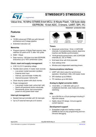
LQFP32
7x7 mm
TSSOP20
6.5x6.4 mm
UFQFPN20
3x3 mm
www.st.com
9. DocID018576 Rev 8 9/103
STM8S003F3 STM8S003K3 Introduction
29
1 Introduction
This datasheet contains the description of the STM8S003F3/K3 value line features, pinout,
electrical characteristics, mechanical data and ordering information.
• For complete information on the STM8S microcontroller memory, registers and
peripherals, please refer to the STM8S and STM8A microcontroller families reference
manual (RM0016).
• For information on programming, erasing and protection of the internal Flash memory
please refer to the PM0051 (How to program STM8S and STM8A Flash program
memory and data EEPROM).
• For information on the debug and SWIM (single wire interface module) refer to the
STM8 SWIM communication protocol and debug module user manual (UM0470).
• For information on the STM8 core, please refer to the STM8 CPU programming manual
(PM0044).
10. Description STM8S003F3 STM8S003K3
10/103 DocID018576 Rev 8
2 Description
The STM8S003F3/K3 value line 8-bit microcontrollers offer 8 Kbytes of Flash program
memory, plus integrated true data EEPROM. They are referred to as low-density devices in
the STM8S microcontroller family reference manual (RM0016).
TheSTM8S003F3/K3 value line devices provide the following benefits: performance,
robustness and reduced system cost.
Device performance and robustness are ensured by true data EEPROM supporting up to
100000 write/erase cycles, advanced core and peripherals made in a state-of-the-art
technology at 16 MHz clock frequency, robust I/Os, independent watchdogs with separate
clock source, and a clock security system.
The system cost is reduced thanks to a high system integration level with internal clock
oscillators, watchdog, and brown-out reset.
Full documentation is offered as well as a wide choice of development tools.
Table 1. STM8S003F3/K3 value line features
Features STM8S003K3 STM8S003F3
Pin count 32 20
Max. number of GPIOs (I/O) 28 16
External interrupt pins 27 16
Timer CAPCOM channels 7 7
Timer complementary outputs 3 2
A/D converter channels 4 5
High-sink I/Os 21 12
Low-density Flash program
memory (byte)
8 K 8 K
RAM (byte) 1 K 1 K
True data EEPROM (byte) 128(1)
1. Without read-while-write capability.
128(1)
Peripheral set
Multi purpose timer (TIM1), SPI, I2C, UART, Window WDG,
independent WDG, ADC, PWM timer (TIM2), 8-bit timer (TIM4)
11. DocID018576 Rev 8 11/103
STM8S003F3 STM8S003K3 Block diagram
29
3 Block diagram
Figure 1. STM8S003F3/K3 value line block diagram
XTAL 1-16 MHz
RC int. 16 MHz
RC int. 128 kHz
STM8 core
Debug/SWIM
UART1
I2C
SPI
AWU timer
Reset block
Reset
POR BOR
Clock controller
Detector
Clock to peripherals and core
400 Kbit/s
8 Mbit/s
up to 5
Addressanddatabus
Window WDG
8 Kbyte
128 byte
1 Kbyte RAM
ADC1
Reset
Single wire
debug interface
program Flash
data EEPROM
16-bit general purpose
16-bit advanced control
timer (TIM1)
timer (TIM2)
8-bit basic timer
(TIM4)
Beeper1/2/4 kHz beep
Independent WDG
4 CAPCOM
channels
Up to
3 CAPCOM
channels
Up to
+ 3 complementary
outputs
LIN master
channels
SPI emul.
12. Product overview STM8S003F3 STM8S003K3
12/103 DocID018576 Rev 8
4 Product overview
The following section intends to give an overview of the basic features of the
STM8S003F3/K3 value line functional modules and peripherals.
For more detailed information please refer to the corresponding family reference manual
(RM0016).
4.1 Central processing unit STM8
The 8-bit STM8 core is designed for code efficiency and performance.
It contains six internal registers which are directly addressable in each execution context, 20
addressing modes including indexed indirect and relative addressing and 80 instructions.
Architecture and registers
• Harvard architecture
• 3-stage pipeline
• 32-bit wide program memory bus - single cycle fetching for most instructions
• X and Y 16-bit index registers - enabling indexed addressing modes with or without
offset and read-modify-write type data manipulations
• 8-bit accumulator
• 24-bit program counter - 16-Mbyte linear memory space
• 16-bit stack pointer - access to a 64 K-level stack
• 8-bit condition code register - 7 condition flags for the result of the last instruction
Addressing
• 20 addressing modes
• Indexed indirect addressing mode for look-up tables located anywhere in the address
space
• Stack pointer relative addressing mode for local variables and parameter passing
Instruction set
• 80 instructions with 2-byte average instruction size
• Standard data movement and logic/arithmetic functions
• 8-bit by 8-bit multiplication
• 16-bit by 8-bit and 16-bit by 16-bit division
• Bit manipulation
• Data transfer between stack and accumulator (push/pop) with direct stack access
• Data transfer using the X and Y registers or direct memory-to-memory transfers
13. DocID018576 Rev 8 13/103
STM8S003F3 STM8S003K3 Product overview
29
4.2 Single wire interface module (SWIM) and debug module (DM)
The single wire interface module and debug module permits non-intrusive, real-time in-
circuit debugging and fast memory programming.
SWIM
Single wire interface module for direct access to the debug module and memory
programming. The interface can be activated in all device operation modes. The maximum
data transmission speed is 145 byte/ms.
Debug module
The non-intrusive debugging module features a performance close to a full-featured
emulator. Beside memory and peripherals, also CPU operation can be monitored in real-
time by means of shadow registers.
• R/W to RAM and peripheral registers in real-time
• R/W access to all resources by stalling the CPU
• Breakpoints on all program-memory instructions (software breakpoints)
• Two advanced breakpoints, 23 predefined configurations
4.3 Interrupt controller
• Nested interrupts with three software priority levels
• 32 interrupt vectors with hardware priority
• Up to 27 external interrupts on six vectors including TLI
• Trap and reset interrupts
4.4 Flash program memory and data EEPROM
• 8 Kbyte of Flash program single voltage Flash memory
• 128 byte true data EEPROM
• User option byte area
Write protection (WP)
Write protection of Flash program memory and data EEPROM is provided to avoid
unintentional overwriting of memory that could result from a user software malfunction.
There are two levels of write protection. The first level is known as MASS (memory access
security system). MASS is always enabled and protects the main Flash program memory,
data EEPROM and option bytes.
To perform in-application programming (IAP), this write protection can be removed by
writing a MASS key sequence in a control register. This allows the application to modify the
content of main program memory and data EEPROM, or to reprogram the device option
bytes.
A second level of write protection, can be enabled to further protect a specific area of
memory known as UBC (user boot code). Refer to Figure 2.
14. Product overview STM8S003F3 STM8S003K3
14/103 DocID018576 Rev 8
The size of the UBC is programmable through the UBC option byte (Table 13), in increments
of 1 page (64-byte block) by programming the UBC option byte in ICP mode.
This divides the program memory into two areas:
• Main program memory: 8 Kbyte minus UBC
• User-specific boot code (UBC): Configurable up to 8 Kbyte
The UBC area remains write-protected during in-application programming. This means that
the MASS keys do not unlock the UBC area. It protects the memory used to store the boot
program, specific code libraries, reset and interrupt vectors, the reset routine and usually
the IAP and communication routines.
Figure 2. Flash memory organization
Read-out protection (ROP)
The read-out protection blocks reading and writing from/to the Flash program memory and
data EEPROM memory in ICP mode (and debug mode). Once the read-out protection is
activated, any attempt to toggle its status triggers a global erase of the program memory.
Even if no protection can be considered as totally unbreakable, the feature provides a very
high level of protection for a general purpose microcontroller.
15. DocID018576 Rev 8 15/103
STM8S003F3 STM8S003K3 Product overview
29
4.5 Clock controller
The clock controller distributes the system clock (fMASTER) coming from different oscillators
to the core and the peripherals. It also manages clock gating for low power modes and
ensures clock robustness.
Features
• Clock prescaler: To get the best compromise between speed and current
consumption the clock frequency to the CPU and peripherals can be adjusted by a
programmable prescaler.
• Safe clock switching: Clock sources can be changed safely on the fly in run mode
through a configuration register. The clock signal is not switched until the new clock
source is ready. The design guarantees glitch-free switching.
• Clock management: To reduce power consumption, the clock controller can stop the
clock to the core, individual peripherals or memory.
• Master clock sources: Four different clock sources can be used to drive the master
clock:
– 1-16 MHz high-speed external crystal (HSE)
– Up to 16 MHz high-speed user-external clock (HSE user-ext)
– 16 MHz high-speed internal RC oscillator (HSI)
– 128 kHz low-speed internal RC (LSI)
• Startup clock: After reset, the microcontroller restarts by default with an internal
2 MHz clock (HSI/8). The prescaler ratio and clock source can be changed by the
application program as soon as the code execution starts.
• Clock security system (CSS): This feature can be enabled by software. If an HSE
clock failure occurs, the internal RC (16 MHz/8) is automatically selected by the CSS
and an interrupt can optionally be generated.
• Configurable main clock output (CCO): This outputs an external clock for use by the
application.
Table 2. Peripheral clock gating bit assignments in CLK_PCKENR1/2 registers
Bit
Peripheral
clock
Bit
Peripheral
clock
Bit
Peripheral
clock
Bit
Peripheral
clock
PCKEN17 TIM1 PCKEN13 UART1 PCKEN27 Reserved PCKEN23 ADC
PCKEN16 Reserved PCKEN12 Reserved PCKEN26 Reserved PCKEN22 AWU
PCKEN15 TIM2 PCKEN11 SPI PCKEN25 Reserved PCKEN21 Reserved
PCKEN14 TIM4 PCKEN10 I2
C PCKEN24 Reserved PCKEN20 Reserved
16. Product overview STM8S003F3 STM8S003K3
16/103 DocID018576 Rev 8
4.6 Power management
For efficient power management, the application can be put in one of four different low-
power modes. You can configure each mode to obtain the best compromise between the
lowest power consumption, the fastest start-up time and available wakeup sources.
• Wait mode: In this mode, the CPU is stopped, but peripherals are kept running. The
wakeup is performed by an internal or external interrupt or reset.
• Active halt mode with regulator on: In this mode, the CPU and peripheral clocks are
stopped. An internal wakeup is generated at programmable intervals by the auto wake
up unit (AWU). The main voltage regulator is kept powered on, so current consumption
is higher than in active halt mode with regulator off, but the wakeup time is faster.
Wakeup is triggered by the internal AWU interrupt, external interrupt or reset.
• Active halt mode with regulator off: This mode is the same as active halt with
regulator on, except that the main voltage regulator is powered off, so the wake up time
is slower.
• Halt mode: In this mode the microcontroller uses the least power. The CPU and
peripheral clocks are stopped, the main voltage regulator is powered off. Wakeup is
triggered by external event or reset.
4.7 Watchdog timers
The watchdog system is based on two independent timers providing maximum security to
the applications.
Activation of the watchdog timers is controlled by option bytes or by software. Once
activated, the watchdogs cannot be disabled by the user program without performing a
reset.
Window watchdog timer
The window watchdog is used to detect the occurrence of a software fault, usually
generated by external interferences or by unexpected logical conditions, which cause the
application program to abandon its normal sequence.
The window function can be used to trim the watchdog behavior to match the application
perfectly.
The application software must refresh the counter before time-out and during a limited time
window.
A reset is generated in two situations:
1. Timeout: at 16 MHz CPU clock the time-out period can be adjusted between 75 µs up
to 64 ms.
2. Refresh out of window: the down-counter is refreshed before its value is lower than the
one stored in the window register.
17. DocID018576 Rev 8 17/103
STM8S003F3 STM8S003K3 Product overview
29
Independent watchdog timer
The independent watchdog peripheral can be used to resolve processor malfunctions due to
hardware or software failures.
It is clocked by the 128 kHz LSI internal RC clock source, and thus stays active even in case
of a CPU clock failure
The IWDG time base spans from 60 µs to 1 s.
4.8 Auto wakeup counter
• Used for auto wakeup from active halt mode
• Clock source: internal 128 kHz internal low frequency RC oscillator or external clock
• LSI clock can be internally connected to TIM1 input capture channel 1 for calibration
4.9 Beeper
The beeper function outputs a signal on the BEEP pin for sound generation. The signal is in
the range of 1, 2 or 4 kHz.
The beeper output port is only available through the alternate function remap option bit
AFR7.
4.10 TIM1 - 16-bit advanced control timer
This is a high-end timer designed for a wide range of control applications. With its
complementary outputs, dead-time control and center-aligned PWM capability, the field of
applications is extended to motor control, lighting and half-bridge driver
• 16-bit up, down and up/down autoreload counter with 16-bit prescaler
• Four independent capture/compare channels (CAPCOM) configurable as input
capture, output compare, PWM generation (edge and center aligned mode) and single
pulse mode output
• Synchronization module to control the timer with external signals
• Break input to force the timer outputs into a defined state
• Three complementary outputs with adjustable dead time
• Encoder mode
• Interrupt sources: 3 x input capture/output compare, 1 x overflow/update, 1 x break
4.11 TIM2 - 16-bit general purpose timer
• 16-bit autoreload (AR) up-counter
• 15-bit prescaler adjustable to fixed power of 2 ratios 1…32768
• 3 individually configurable capture/compare channels
• PWM mode
• Interrupt sources: 3 x input capture/output compare, 1 x overflow/update
18. Product overview STM8S003F3 STM8S003K3
18/103 DocID018576 Rev 8
4.12 TIM4 - 8-bit basic timer
• 8-bit autoreload, adjustable prescaler ratio to any power of 2 from 1 to 128
• Clock source: CPU clock
• Interrupt source: 1 x overflow/update
4.13 Analog-to-digital converter (ADC1)
STM8S003F3/K3 value line products contain a 10-bit successive approximation A/D
converter (ADC1) with up to 5 external multiplexed input channels and the following main
features:
• Input voltage range: 0 to VDDA
• Conversion time: 14 clock cycles
• Single and continuous, buffered continuous conversion modes
• Buffer size (10 x 10 bits)
• Scan mode for single and continuous conversion of a sequence of channels
• Analog watchdog capability with programmable upper and lower thresholds
• Analog watchdog interrupt
• External trigger input
• Trigger from TIM1 TRGO
• End of conversion (EOC) interrupt
Note: Additional AIN12 analog input is not selectable in ADC scan mode or with analog watchdog.
Values converted from AIN12 are stored only into the ADC_DRH/ADC_DRL registers.
4.14 Communication interfaces
The following communication interfaces are implemented:
• UART1: full feature UART, synchronous mode, SPI master mode, SmartCard mode,
IrDA mode, LIN2.1 master capability
• SPI: full and half-duplex, 8 Mbit/s
• I²C: up to 400 Kbit/s
Table 3. TIM timer features
Timer
Counter
size
(bits)
Prescaler
Counting
mode
CAPCOM
channels
Complem.
outputs
Ext.
trigger
Timer
synchr-
onization/
chaining
TIM1 16 Any integer from 1 to 65536 Up/down 4 3 Yes
NoTIM2 16 Any power of 2 from 1 to 32768 Up 3 0 No
TIM4 8 Any power of 2 from 1 to 128 Up 0 0 No
19. DocID018576 Rev 8 19/103
STM8S003F3 STM8S003K3 Product overview
29
4.14.1 UART1
Main features
• 1 Mbit/s full duplex SCI
• SPI emulation
• High precision baud rate generator
• Smartcard emulation
• IrDA SIR encoder decoder
• LIN master mode
• Single wire half duplex mode
Asynchronous communication (UART mode)
• Full duplex communication - NRZ standard format (mark/space)
• Programmable transmit and receive baud rates up to 1 Mbit/s (fCPU/16) and capable of
following any standard baud rate regardless of the input frequency
• Separate enable bits for transmitter and receiver
• Two receiver wakeup modes:
– Address bit (MSB)
– Idle line (interrupt)
• Transmission error detection with interrupt generation
• Parity control
Synchronous communication
• Full duplex synchronous transfers
• SPI master operation
• 8-bit data communication
• Maximum speed: 1 Mbit/s at 16 MHz (fCPU/16)
LIN master mode
• Emission: generates 13-bit synch. break frame
• Reception: detects 11-bit break frame
4.14.2 SPI
• Maximum speed: 8 Mbit/s (fMASTER/2) both for master and slave
• Full duplex synchronous transfers
• Simplex synchronous transfers on two lines with a possible bidirectional data line
• Master or slave operation - selectable by hardware or software
• CRC calculation
• 1 byte Tx and Rx buffer
• Slave/master selection input pin
20. Product overview STM8S003F3 STM8S003K3
20/103 DocID018576 Rev 8
4.14.3 I2
C
• I2C master features
– Clock generation
– Start and stop generation
• I2C slave features
– Programmable I2C address detection
– Stop bit detection
• Generation and detection of 7-bit/10-bit addressing and general call
• Supports different communication speeds
– Standard speed (up to 100 kHz)
– Fast speed (up to 400 kHz)
21. DocID018576 Rev 8 21/103
STM8S003F3 STM8S003K3 Pinouts and pin descriptions
29
5 Pinouts and pin descriptions
Table 4. Legend/abbreviations for STM8S003F3/K3 pin description tables
Type I = input, O = output, S = power supply
Level
Input CM = CMOS
Output HS = high sink
Output speed
O1 = slow (up to 2 MHz)
O2 = fast (up to 10 MHz)
O3 = fast/slow programmability with slow as default state after reset
O4 = fast/slow programmability with fast as default state after reset
Port and control
configuration
Input float = floating, wpu = weak pull-up
Output T = true open drain, OD = open drain, PP = push pull
Reset state
Bold x (pin state after internal reset release)
Unless otherwise specified, the pin state is the same during the reset phase
and after the internal reset release.
22. Pinouts and pin descriptions STM8S003F3 STM8S003K3
22/103 DocID018576 Rev 8
5.1 STM8S003K3 LQFP32 pinout and pin description
Figure 3. STM8S003K3 LQFP32 pinout
Table 5. STM8S003K3 descriptions
LQFP32
Pin name
Type
Input Output
Mainfunction
(afterreset)
Default
alternate
function
Alternate
function
after remap
[option bit]
floating
wpu
Ext.interrupt
Highsink(1)
Speed
OD
PP
1 NRST I/O - X - - - - - Reset -
2 PA1/OSCIN(2) I/O X X X - O1 X X Port A1
Resonator/
crystal in
-
23. DocID018576 Rev 8 23/103
STM8S003F3 STM8S003K3 Pinouts and pin descriptions
29
3 PA2/OSCOUT I/O X X X - O1 X X Port A2
Resonator/
crystal out
-
4 VSS S - - - - - - - Digital ground -
5 VCAP S - - - - - - - 1.8 V regulator capacitor -
6 VDD S - - - - - - - Digital power supply -
7
PA3/TIM2_CH3
[SPI_NSS]
I/O X X X HS O3 X X Port A3
Timer 2
channel 3
SPI master/
slave select
[AFR1]
8 PF4 I/O X X - - O1 X X Port F4 - -
9 PB7 I/O X X - - O1 X X Port B7 - -
10 PB6 I/O X X - - O1 X X Port B6 - -
11 PB5/I2
C_SDA I/O X - X - O1 T(3)
- Port B5 I2
C data -
12 PB4/I2C_SCL I/O X - X - O1 T(3) - Port B4 I2C clock -
13
PB3/AIN3
[TIM1_ETR]
I/O X X X HS O3 X X Port B3
Analog
input 3/Timer 1
external trigger
-
14
PB2/AIN2
[TIM1_CH3N]
I/O X X X HS O3 X X Port B2
Analog
input 2/Timer 1
- inverted
channel 3
-
15
PB1/AIN1
[TIM1_CH2N]
I/O X X X HS O3 X X Port B1
Analog
input 1/Timer 1
- inverted
channel 2
-
16
PB0/AIN0
[TIM1_CH1N]
I/O X X X HS O3 X X Port B0
Analog
input 0/Timer 1
- inverted
channel 1
-
17 PE5/SPI_NSS I/O X X X HS O3 X X Port E5
SPI
master/slave
select
-
18
PC1/TIM1_CH1/
UART1_CK
I/O X X X HS O3 X X Port C1
Timer 1 -
channel 1
UART1 clock
-
19 PC2/TIM1_CH2 I/O X X X HS O3 X X Port C2
Timer 1-
channel 2
-
20 PC3/TIM1_CH3 I/O X X X HS O3 X X Port C3
Timer 1 -
channel 3
-
Table 5. STM8S003K3 descriptions (continued)
LQFP32
Pin name
Type
Input Output
Mainfunction
(afterreset)
Default
alternate
function
Alternate
function
after remap
[option bit]
floating
wpu
Ext.interrupt
Highsink(1)
Speed
OD
PP
24. Pinouts and pin descriptions STM8S003F3 STM8S003K3
24/103 DocID018576 Rev 8
21
PC4/TIM1_CH4/C
LK_CCO
I/O X X X HS O3 X X Port C4
Timer 1 -
channel
4/configurable
clock output
-
22 PC5/SPI_SCK I/O X X X HS O3 X X Port C5 SPI clock -
23 PC6/SPI_MOSI I/O X X X HS O3 X X Port C6
SPI master
out/slave in
-
24 PC7/SPI_MISO I/O X X X HS O3 X X Port C7
SPI master in/
slave out
-
25
PD0/[TIM1_BKIN
[CLK_CCO]
I/O X X X HS O3 X X Port D0
Timer 1 - break
input
Configurable
clock output
[AFR5]
26 PD1/SWIM(4)
I/O X X X HS O4 X X Port D1
SWIM data
interface
-
27
PD2
[TIM2_CH3]
I/O X X X HS O3 X X Port D2 -
Timer 2 -
channel 3
[AFR1]
28
PD3/TIM2_CH2
[ADC_ETR]
I/O X X X HS O3 X X Port D3
Timer 2 -
channel2/ADC
external trigger
-
29
PD4/BEEP/
TIM2_CH1
I/O X X X HS O3 X X Port D4
Timer 2 -
channel
1/BEEP output
-
30 PD5/ UART1_TX I/O X X X HS O3 X X Port D5
UART1 data
transmit
-
31 PD6/ UART1_RX I/O X X X HS O3 X X Port D6
UART1 data
receive
-
32
PD7/TLI
[TIM1_CH4]
I/O X X X HS O3 X X Port D7
Top level
interrupt
Timer 1 -
channel 4
[AFR6]
1. I/O pins used simultaneously for high-current source/sink must be uniformly spaced around the package. In
addition, the total driven current must respect the absolute maximum ratings given in Section 9: Electrical
characteristics.
2. When the MCU is in Halt/Active-halt mode, PA1 is automatically configured in input weak pull-up and
cannot be used for waking up the device. In this mode, the output state of PA1 is not driven. It is
recommended to use PA1 only in input mode if Halt/Active-halt is used in the application.
3. In the open-drain output column, "T" defines a true open-drain I/O (P-buffer, weak pull-up, and protection
diode to VDD are not implemented).
4. The PD1 pin is in input pull-up during the reset phase and after the internal reset release.
Table 5. STM8S003K3 descriptions (continued)
LQFP32
Pin name
Type
Input Output
Mainfunction
(afterreset)
Default
alternate
function
Alternate
function
after remap
[option bit]
floating
wpu
Ext.interrupt
Highsink(1)
Speed
OD
PP
25. DocID018576 Rev 8 25/103
STM8S003F3 STM8S003K3 Pinouts and pin descriptions
29
5.2 STM8S003F3 TSSOP20/UFQFPN20 pinout and pin
description
Figure 4. STM8S003F3 TSSOP20 pinout
1. HS high sink capability.
2. (T) True open drain (P-buffer and protection diode to VDD not implemented).
3. [ ] alternate function remapping option (If the same alternate function is shown twice, it indicates an
exclusive choice not a duplication of the function).
26. Pinouts and pin descriptions STM8S003F3 STM8S003K3
26/103 DocID018576 Rev 8
Figure 5. STM8S003F3 UFQFPN20 pinout
1. HS high sink capability.
2. (T) True open drain (P-buffer and protection diode to VDD not implemented).
3. [ ] alternate function remapping option (If the same alternate function is shown twice, it indicates an
exclusive choice not a duplication of the function).
27. DocID018576 Rev 8 27/103
STM8S003F3 STM8S003K3 Pinouts and pin descriptions
29
Table 6. STM8S003F3 pin description
Pin
no.
Pin name Type
Input Output
Main
function
(after
reset)
Default
alternate
function
Alternate
function
after remap
[option bit]
TSSOP20
UFQFPN20
floating
wpu
Ext.interr.
High
sink(1)
Speed
OD PP
1 18
PD4/ BEEP/
TIM2_ CH1/
UART1 _CK
I/O X X X HS O3 X X Port D4
Timer 2 -
channel
1/BEEP
output/
UART1clock
-
2 19
PD5/ AIN5/
UART1 _TX
I/O X X X HS O3 X X Port D5
Analog input
5/ UART1
data transmit
-
3 20
PD6/ AIN6/
UART1 _RX
I/O X X X HS O3 X X Port D6
Analog input
6/ UART1
data receive
-
4 1 NRST I/O - X - - - - - Reset -
5 2 PA1/ OSCIN(2) I/O X X X - O1 X X Port A1
Resonator/
crystal in
-
6 3 PA2/ OSCOUT I/O X X X - O1 X X Port A2
Resonator/
crystal out
-
7 4 VSS S - - - - - - - Digital ground -
8 5 VCAP S - - - - - - -
1.8 V regulator
capacitor
-
9 6 VDD S - - - - - - - Digital power supply -
10
7
PA3/ TIM2_ CH3
[SPI_ NSS]
I/O X X X HS O3 X X Port A3
Timer 2
channel 3
SPI master/
slave select
[AFR1]
11
8
PB5/ I2C_ SDA
[TIM1_ BKIN]
I/O X - X - O1 T(3) - Port B5 I2C data
Timer 1 -
break input
[AFR4]
12
9 PB4/ I2C_ SCL I/O X - X - O1 T(3) - Port B4 I2C clock
ADC
external
trigger
[AFR4]
13
10
PC3/ TIM1_CH3
[TLI]
[TIM1_ CH1N]
I/O X X X HS O3 X X Port C3
Timer 1 -
channel 3
Top level
interrupt
[AFR3]
Timer 1 -
inverted
channel 1
[AFR7]
28. Pinouts and pin descriptions STM8S003F3 STM8S003K3
28/103 DocID018576 Rev 8
14
11
PC4/CLK_CCO/
TIM1_
CH4/AIN2/
[TIM1_ CH2N]
I/O X X X HS O3 X X Port C4
Configurable
clock
output/Timer
1 - channel
4/Analog
input 2
Timer 1 -
inverted
channel 2
[AFR7]
15
12
PC5/ SPI_SCK
[TIM2_ CH1]
I/O X X X HS O3 X X Port C5 SPI clock
Timer 2 -
channel 1
[AFR0]
16
13
PC6/ SPI_MOSI
[TIM1_ CH1]
I/O X X X HS O3 X X Port C6
SPI master
out/slave in
Timer 1 -
channel 1
[AFR0]
17
14
PC7/ SPI_MISO
[TIM1_ CH2]
I/O X X X HS O3 X X Port C7
SPI master
in/ slave out
Timer 1 -
channel 2
[AFR0]
18
15 PD1/ SWIM(4) I/O X X X HS O4 X X Port D1
SWIM data
interface
-
19
16
PD2/AIN3/
[TIM2_ CH3]
I/O X X X HS O3 X X Port D2
Analog input
3
Timer 2 -
channel 3
[AFR1]
20
17
PD3/ AIN4/
TIM2_ CH2/
ADC_ ETR
I/O X X X HS O3 X X Port D3
Analog input
4/ Timer 2 -
channel
2/ADC
external
trigger
-
1. I/O pins used simultaneously for high current source/sink must be uniformly spaced around the package. In addition, the
total driven current must respect the absolute maximum ratings.
2. When the MCU is in halt/active-halt mode, PA1 is automatically configured in input weak pull-up and cannot be used for
waking up the device. In this mode, the output state of PA1 is not driven. It is recommended d to use PA1 only in input mode
if halt/active-halt is used in the application.
3. In the open-drain output column, "T" defines a true open-drain I/O (P-buffer, weak pull-up, and protection diode to VDD are
not implemented).
4. The PD1 pin is in input pull-up during the reset phase and after internal reset release.
Table 6. STM8S003F3 pin description (continued)
Pin
no.
Pin name Type
Input Output
Main
function
(after
reset)
Default
alternate
function
Alternate
function
after remap
[option bit]
TSSOP20
UFQFPN20
floating
wpu
Ext.interr.
High
sink(1)
Speed
OD PP
29. DocID018576 Rev 8 29/103
STM8S003F3 STM8S003K3 Pinouts and pin descriptions
29
5.3 Alternate function remapping
As shown in the rightmost column of the pin description table, some alternate functions can
be remapped at different I/O ports by programming one of eight AFR (alternate function
remap) option bits. Refer to Section 8: Option bytes. When the remapping option is active,
the default alternate function is no longer available.
To use an alternate function, the corresponding peripheral must be enabled in the peripheral
registers.
Alternate function remapping does not effect GPIO capabilities of the I/O ports (see the
GPIO section of the family reference manual, RM0016).
31. DocID018576 Rev 8 31/103
STM8S003F3 STM8S003K3 Memory and register map
41
Table 7 lists the boundary addresses for each memory size. The top of the stack is at the
RAM end address in each case.
6.2 Register map
6.2.1 I/O port hardware register map
Table 7. Flash, Data EEPROM and RAM boundary addresses
Memory area Size (byte) Start address End address
Flash program memory 8 K 0x00 8000 0x00 9FFF
RAM 1 K 0x00 0000 0x00 03FF
Data EEPROM 128 0x00 4000 0x00 407F
Table 8. I/O port hardware register map
Address Block Register label Register name
Reset
status
0x00 5000
Port A
PA_ODR Port A data output latch register 0x00
0x00 5001 PA_IDR Port A input pin value register 0xXX(1)
0x00 5002 PA_DDR Port A data direction register 0x00
0x00 5003 PA_CR1 Port A control register 1 0x00
0x00 5004 PA_CR2 Port A control register 2 0x00
0x00 5005
Port B
PB_ODR Port B data output latch register 0x00
0x00 5006 PB_IDR Port B input pin value register 0xXX(1)
0x00 5007 PB_DDR Port B data direction register 0x00
0x00 5008 PB_CR1 Port B control register 1 0x00
0x00 5009 PB_CR2 Port B control register 2 0x00
0x00 500A
Port C
PC_ODR Port C data output latch register 0x00
0x00 500B PB_IDR Port C input pin value register 0xXX(1)
0x00 500C PC_DDR Port C data direction register 0x00
0x00 500D PC_CR1 Port C control register 1 0x00
0x00 500E PC_CR2 Port C control register 2 0x00
0x00 500F
Port D
PD_ODR Port D data output latch register 0x00
0x00 5010 PD_IDR Port D input pin value register 0xXX(1)
0x00 5011 PD_DDR Port D data direction register 0x00
0x00 5012 PD_CR1 Port D control register 1 0x02
0x00 5013 PD_CR2 Port D control register 2 0x00
32. Memory and register map STM8S003F3 STM8S003K3
32/103 DocID018576 Rev 8
6.2.2 General hardware register map
0x00 5014
Port E
PE_ODR Port E data output latch register 0x00
0x00 5015 PE_IDR Port E input pin value register 0xXX(1)
0x00 5016 PE_DDR Port E data direction register 0x00
0x00 5017 PE_CR1 Port E control register 1 0x00
0x00 5018 PE_CR2 Port E control register 2 0x00
0x00 5019
Port F
PF_ODR Port F data output latch register 0x00
0x00 501A PF_IDR Port F input pin value register 0xXX(1)
0x00 501B PF_DDR Port F data direction register 0x00
0x00 501C PF_CR1 Port F control register 1 0x00
0x00 501D PF_CR2 Port F control register 2 0x00
1. Depends on the external circuitry.
Table 8. I/O port hardware register map (continued)
Address Block Register label Register name
Reset
status
33. DocID018576 Rev 8 33/103
STM8S003F3 STM8S003K3 Memory and register map
41
Table 9. General hardware register map
Address Block Register label Register name
Reset
status
0x00 501E to
0x00 5059
Reserved area (60 byte)
0x00 505A
Flash
FLASH_CR1 Flash control register 1 0x00
0x00 505B FLASH_CR2 Flash control register 2 0x00
0x00 505C FLASH_NCR2 Flash complementary control register 2 0xFF
0x00 505D FLASH _FPR Flash protection register 0x00
0x00 505E FLASH _NFPR Flash complementary protection register 0xFF
0x00 505F FLASH _IAPSR
Flash in-application programming status
register
0x00
0x00 5060 to
0x00 5061
Reserved area (2 byte)
0x00 5062 Flash FLASH _PUKR
Flash Program memory unprotection
register
0x00
0x00 5063 Reserved area (1 byte)
0x00 5064 Flash FLASH _DUKR Data EEPROM unprotection register 0x00
0x00 5065 to
0x00 509F
Reserved area (59 byte)
0x00 50A0
ITC
EXTI_CR1 External interrupt control register 1 0x00
0x00 50A1 EXTI_CR2 External interrupt control register 2 0x00
0x00 50A2 to
0x00 50B2
Reserved area (17 byte)
0x00 50B3 RST RST_SR Reset status register 0xXX(1)
0x00 50B4 to
0x00 50BF
Reserved area (12 byte)
0x00 50C0
CLK
CLK_ICKR Internal clock control register 0x01
0x00 50C1 CLK_ECKR External clock control register 0x00
0x00 50C2 Reserved area (1 byte)
0x00 50C3
CLK
CLK_CMSR Clock master status register 0xE1
0x00 50C4 CLK_SWR Clock master switch register 0xE1
0x00 50C5 CLK_SWCR Clock switch control register 0xXX
0x00 50C6 CLK_CKDIVR Clock divider register 0x18
0x00 50C7 CLK_PCKENR1 Peripheral clock gating register 1 0xFF
0x00 50C8 CLK_CSSR Clock security system register 0x00
0x00 50C9 CLK_CCOR Configurable clock control register 0x00
0x00 50CA CLK_PCKENR2 Peripheral clock gating register 2 0xFF
0x00 50CB Reserved area (1 byte)
34. Memory and register map STM8S003F3 STM8S003K3
34/103 DocID018576 Rev 8
0x00 50CC
CLK
CLK_HSITRIMR HSI clock calibration trimming register 0x00
0x00 50CD CLK_SWIMCCR SWIM clock control register
0bXXXX
XXX0
0x00 50CE to
0x00 50D0
Reserved area (3 byte)
0x00 50D1
WWDG
WWDG_CR WWDG control register 0x7F
0x00 50D2 WWDG_WR WWDR window register 0x7F
0x00 50D3 to
0x00 50DF
Reserved area (13 byte)
0x00 50E0
IWDG
IWDG_KR IWDG key register 0xXX(2)
0x00 50E1 IWDG_PR IWDG prescaler register 0x00
0x00 50E2 IWDG_RLR IWDG reload register 0xFF
0x00 50E3 to
0x00 50EF
Reserved area (13 byte)
0x00 50F0
AWU
AWU_CSR1 AWU control/status register 1 0x00
0x00 50F1 AWU_APR AWU asynchronous prescaler buffer register 0x3F
0x00 50F2 AWU_TBR AWU timebase selection register 0x00
0x00 50F3 BEEP BEEP_CSR BEEP control/status register 0x1F
0x00 50F4 to
0x00 50FF
Reserved area (12 byte)
0x00 5200
SPI
SPI_CR1 SPI control register 1 0x00
0x00 5201 SPI_CR2 SPI control register 2 0x00
0x00 5202 SPI_ICR SPI interrupt control register 0x00
0x00 5203 SPI_SR SPI status register 0x02
0x00 5204 SPI_DR SPI data register 0x00
0x00 5205 SPI_CRCPR SPI CRC polynomial register 0x07
0x00 5206 SPI_RXCRCR SPI Rx CRC register 0x00
0x00 5207 SPI_TXCRCR SPI Tx CRC register 0x00
0x00 5208 to
0x00 520F
Reserved area (8 byte)
0x00 5210
I2
C
I2C_CR1 I2
C control register 1 0x00
0x00 5211 I2C_CR2 I2
C control register 2 0x00
0x00 5212 I2C_FREQR I2
C frequency register 0x00
0x00 5213 I2C_OARL I2
C own address register low 0x00
0x00 5214 I2C_OARH I2
C own address register high 0x00
0x00 5215 Reserved
Table 9. General hardware register map (continued)
Address Block Register label Register name
Reset
status
35. DocID018576 Rev 8 35/103
STM8S003F3 STM8S003K3 Memory and register map
41
0x00 5216
I2
C
I2C_DR I2
C data register 0x00
0x00 5217 I2C_SR1 I2
C status register 1 0x00
0x00 5218 I2C_SR2 I2
C status register 2 0x00
0x00 5219 I2C_SR3 I2
C status register 3 0x00
0x00 521A I2C_ITR I2
C interrupt control register 0x00
0x00 521B I2C_CCRL I2
C clock control register low 0x00
0x00 521C I2C_CCRH I2
C clock control register high 0x00
0x00 521D I2C_TRISER I2
C TRISE register 0x02
0x00 521E I2C_PECR I2
C packet error checking register 0x00
0x00 521F to
0x00 522F
Reserved area (17 byte)
0x00 5230
UART1
UART1_SR UART1 status register 0xC0
0x00 5231 UART1_DR UART1 data register 0xXX
0x00 5232 UART1_BRR1 UART1 baud rate register 1 0x00
0x00 5233 UART1_BRR2 UART1 baud rate register 2 0x00
0x00 5234 UART1_CR1 UART1 control register 1 0x00
0x00 5235 UART1_CR2 UART1 control register 2 0x00
0x00 5236 UART1_CR3 UART1 control register 3 0x00
0x00 5237 UART1_CR4 UART1 control register 4 0x00
0x00 5238 UART1_CR5 UART1 control register 5 0x00
0x00 5239 UART1_GTR UART1 guard time register 0x00
0x00 523A UART1_PSCR UART1 prescaler register 0x00
0x00 523B to
0x00523F
Reserved area (21 byte)
Table 9. General hardware register map (continued)
Address Block Register label Register name
Reset
status
41. DocID018576 Rev 8 41/103
STM8S003F3 STM8S003K3 Interrupt vector mapping
41
7 Interrupt vector mapping
Table 11. Interrupt mapping
IRQ
no.
Source
block
Description
Wakeup from
Halt mode
Wakeup from
Active-halt mode
Vector address
- RESET Reset Yes Yes 0x00 8000
- TRAP Software interrupt - - 0x00 8004
0 TLI External top level interrupt - - 0x00 8008
1 AWU Auto wake up from halt - Yes 0x00 800C
2 CLK Clock controller - - 0x00 8010
3 EXTI0 Port A external interrupts Yes(1)
Yes(1)
0x00 8014
4 EXTI1 Port B external interrupts Yes Yes 0x00 8018
5 EXTI2 Port C external interrupts Yes Yes 0x00 801C
6 EXTI3 Port D external interrupts Yes Yes 0x00 8020
7 EXTI4 Port E external interrupts Yes Yes 0x00 8024
8 - Reserved 0x00 8028
9 - Reserved 0x00 802C
10 SPI End of transfer Yes Yes 0x00 8030
11 TIM1
TIM1 update/overflow/underflow/
trigger/break
- - 0x00 8034
12 TIM1 TIM1 capture/compare - - 0x00 8038
13 TIM2 TIM2 update /overflow - - 0x00 803C
14 TIM2 TIM2 capture/compare - - 0x00 8040
15 - Reserved 0x00 8044
16 - Reserved 0x00 8048
17 UART1 Tx complete - - 0x00 804C
18 UART1 Receive register DATA FULL - - 0x00 8050
19 I2C I2C interrupt Yes Yes 0x00 8054
20 - Reserved 0x00 8058
21 - Reserved 0x00 805C
22 ADC1
ADC1 end of conversion/analog
watchdog interrupt
- - 0x00 8060
23 TIM4 TIM4 update/overflow - - 0x00 8064
24 Flash EOP/WR_PG_DIS - - 0x00 8068
Reserved
0x00 806C to
0x00 807C
1. Except PA1
42. Option bytes STM8S003F3 STM8S003K3
42/103 DocID018576 Rev 8
8 Option bytes
Option bytes contain configurations for device hardware features as well as the memory
protection of the device. They are stored in a dedicated block of the memory. Except for the
ROP (read-out protection) byte, each option byte has to be stored twice, in a regular form
(OPTx) and a complemented one (NOPTx) for redundancy.
Option bytes can be modified in ICP mode (via SWIM) by accessing the EEPROM address
shown in Table 12: Option bytes below. Option bytes can also be modified ‘on the fly’ by the
application in IAP mode, except the ROP option that can only be modified in ICP mode (via
SWIM).
Refer to the STM8S Flash programming manual (PM0051) and STM8 SWIM
communication protocol and debug module user manual (UM0470) for information on SWIM
programming procedures.
Table 12. Option bytes
Addr.
Option
name
Option
byte no.
Option bits Factory
default
setting7 6 5 4 3 2 1 0
0x4800
Read-out
protection
(ROP)
OPT0 ROP[7:0] 0x00
0x4801
User boot code
(UBC)
OPT1 UBC[7:0] 0x00
0x4802 NOPT1 NUBC[7:0] 0xFF
0x4803 Alternate
function
remapping
(AFR)
OPT2 AFR7 AFR6 AFR5 AFR4 AFR3 AFR2 AFR1 AFR0 0x00
0x4804 NOPT2 NAFR7 NAFR6 NAFR5 NAFR4 NAFR3 NAFR2 NAFR1 NAFR0 0xFF
0x4805
Misc. option
OPT3 Reserved HSITRIM
LSI
_EN
IWDG
_HW
WWDG
_HW
WWDG
_HALT
0x00
0x4806 NOPT3 Reserved
NHSI
TRIM
NLSI
_EN
NIWDG
_HW
NWWDG
_HW
NWWDG
_HALT
0xFF
0x4807
Clock option
OPT4 Reserved
EXT
CLK
CKAWU
SEL
PRS
C1
PRS
C0
0x00
0x4808 NOPT4 Reserved
NEXT
CLK
NCKAW
USEL
NPR
SC1
NPR
SC0
0xFF
0x4809
HSE clock
startup
OPT5 HSECNT[7:0] 0x00
0x480A NOPT5 NHSECNT[7:0] 0xFF
Table 13. Option byte description
Option byte no. Description
OPT0
ROP[7:0] Memory readout protection (ROP)
0xAA: Enable readout protection (write access via SWIM protocol)
Note: Refer to the family reference manual (RM0016) section on
Flash/EEPROM memory readout protection for details.
43. DocID018576 Rev 8 43/103
STM8S003F3 STM8S003K3 Option bytes
45
OPT1
UBC[7:0] User boot code area
0x00: no UBC, no write-protection
0x01: Pages 0 defined as UBC, memory write-protected
0x02: Pages 0 to 1 defined as UBC, memory write-protected
Page 0 and page 1 contain the interrupt vectors.
...
0x7F: Pages 0 to 126 defined as UBC, memory write-protected
Other values: Pages 0 to 127 defined as UBC, memory-write protected.
Note: Refer to the family reference manual (RM0016) section on
Flash/EEPROM write protection for more details.
OPT2
AFR[7:0]
Refer to the following section for alternate function remapping descriptions
of bits [7:2] and [1:0] respectively.
OPT3
HSITRIM: high-speed internal clock trimming register size
0: 3-bit trimming supported in CLK_HSITRIMR register
1: 4-bit trimming supported in CLK_HSITRIMR register
LSI_EN: Low speed internal clock enable
0: LSI clock is not available as CPU clock source
1: LSI clock is available as CPU clock source
IWDG_HW: Independent watchdog
0: IWDG Independent watchdog activated by software
1: IWDG Independent watchdog activated by hardware
WWDG_HW: Window watchdog activation
0: WWDG window watchdog activated by software
1: WWDG window watchdog activated by hardware
WWDG_HALT: Window watchdog reset on halt
0: No reset generated on halt if WWDG active
1: Reset generated on halt if WWDG active
OPT4
EXTCLK: External clock selection
0: External crystal connected to OSCIN/OSCOUT
1: External clock signal on OSCIN
CKAWUSEL: Auto wakeup unit/clock
0: LSI clock source selected for AWU
1: HSE clock with prescaler selected as clock source for for AWU
PRSC[1:0] AWU clock prescaler
0x: 16 MHz to 128 kHz prescaler
10: 8 MHz to 128 kHz prescaler
11: 4 MHz to 128 kHz prescaler
OPT5
HSECNT[7:0]: HSE crystal oscillator stabilization time
This configures the stabilization time.
0x00: 2048 HSE cycles
0xB4: 128 HSE cycles
0xD2: 8 HSE cycles
0xE1: 0.5 HSE cycles
Table 13. Option byte description (continued)
Option byte no. Description
44. Option bytes STM8S003F3 STM8S003K3
44/103 DocID018576 Rev 8
8.1 Alternate function remapping bits
Table 14. STM8S003K3 alternate function remapping bits for 32-pin devices
Option byte number Description(1)
1. Do not use more than one remapping option in the same port. It is forbidden to enable both AFR1 and
AFR0
OPT2
AFR7Alternate function remapping option 7
Reserved.
AFR6 Alternate function remapping option 6
0: AFR6 remapping option inactive: default alternate function(2)
1: Port D7 alternate function = TIM1_CH4.
AFR5 Alternate function remapping option 5
0: AFR5 remapping option inactive: default alternate function(2)
1: Port D0 alternate function = CLK_CCO.
AFR[4:2] Alternate function remapping option 4:2
Reserved.
AFR1 Alternate function remapping option 1
0: AFR1 remapping option inactive: default alternate function(2)
1: Port A3 alternate function = SPI_NSS; port D2 alternate function
TIM2_CH3
AFR0 Alternate function remapping option 0
Reserved.
2. Refer to the pinout description.
45. DocID018576 Rev 8 45/103
STM8S003F3 STM8S003K3 Option bytes
45
Table 15. STM8S003F3 alternate function remapping bits for 20-pin devices
Option byte number Description
OPT2
AFR7Alternate function remapping option 7
0: AFR7 remapping option inactive: default alternate function(1)
1: Port C3 alternate function = TIM1_CH1N; port C4 alternate function =
TIM1_CH2N.
AFR6 Alternate function remapping option 6
Reserved.
AFR5 Alternate function remapping option 5
Reserved.
AFR4 Alternate function remapping option 4
0: AFR4 remapping option inactive: default alternate function(1)
.
1: Port B4 alternate function = ADC_ETR; port B5 alternate function =
TIM1_BKIN.
AFR3 Alternate function remapping option 3
0: AFR3 remapping option inactive: default alternate function(1)
1: Port C3 alternate function = TLI.
AFR2 Alternate function remapping option 2
Reserved.
AFR1 Alternate function remapping option 1 (2)
0: AFR1 remapping option inactive: default alternate function(1)
1: Port A3 alternate function = SPI_NSS; port D2 alternate function =
TIM2_CH3.
AFR0 Alternate function remapping option 0(2)
0: AFR0 remapping option inactive: Default alternate functions(1)
1: Port C5 alternate function = TIM2_CH1; port C6 alternate function =
TIM1_CH1; port C7 alternate function = TIM1_CH2.
1. Refer to the pinout description.
2. Do not use more than one remapping option in the same port. It is forbidden to enable both AFR1 and
AFR0.
46. Electrical characteristics STM8S003F3 STM8S003K3
46/103 DocID018576 Rev 8
9 Electrical characteristics
9.1 Parameter conditions
Unless otherwise specified, all voltages are referred to VSS.
9.1.1 Minimum and maximum values
Unless otherwise specified the minimum and maximum values are guaranteed in the worst
conditions of ambient temperature, supply voltage and frequencies by tests in production on
100% of the devices with an ambient temperature at TA = 25 °C and TA = TAmax (given by
the selected temperature range).
Data based on characterization results, design simulation and/or technology characteristics
are indicated in the table footnotes and are not tested in production. Based on
characterization, the minimum and maximum values refer to sample tests and represent the
mean value plus or minus three times the standard deviation (mean ± 3 Σ).
9.1.2 Typical values
Unless otherwise specified, typical data are based on TA = 25 °C, VDD = 5 V. They are given
only as design guidelines and are not tested.
Typical ADC accuracy values are determined by characterization of a batch of samples from
a standard diffusion lot over the full temperature range, where 95% of the devices have an
error less than or equal to the value indicated (mean ± 2 Σ).
9.1.3 Typical curves
Unless otherwise specified, all typical curves are given only as design guidelines and are
not tested.
9.1.4 Loading capacitor
The loading conditions used for pin parameter measurement are shown in Figure 7.
Figure 7. Pin loading conditions
9.1.5 Pin input voltage
The input voltage measurement on a pin of the device is described in Figure 8.
50 pF
STM8 pin
47. DocID018576 Rev 8 47/103
STM8S003F3 STM8S003K3 Electrical characteristics
87
Figure 8. Pin input voltage
9.2 Absolute maximum ratings
Stresses above those listed as ‘absolute maximum ratings’ may cause permanent damage
to the device. This is a stress rating only and functional operation of the device under these
conditions is not implied. Exposure to maximum rating conditions for extended periods may
affect device reliability.
VIN
STM8 pin
Table 16. Voltage characteristics
Symbol Ratings Min Max Unit
VDDx - VSS Supply voltage(1)
1. All power (VDD) and ground (VSS) pins must always be connected to the external power supply
-0.3 6.5
V
VIN
Input voltage on true open drain pins(2)
2. IINJ(PIN) must never be exceeded. This is implicitly insured if VIN maximum is respected. If VIN maximum
cannot be respected, the injection current must be limited externally to the IINJ(PIN) value. A positive
injection is induced by VIN>VDD while a negative injection is induced by VIN<VSS. For true open-drain pads,
there is no positive injection current, and the corresponding VIN maximum must always be respected
VSS - 0.3 6.5
Input voltage on any other pin(2)
VSS - 0.3 VDD + 0.3
|VDDx - VDD| Variations between different power pins - 50
mV
|VSSx - VSS| Variations between all the different ground pins - 50
VESD Electrostatic discharge voltage
see Absolute maximum
ratings (electrical
sensitivity) on page 86
-
48. Electrical characteristics STM8S003F3 STM8S003K3
48/103 DocID018576 Rev 8
Table 17. Current characteristics
Symbol Ratings Max.(1)
1. Data based on characterization results, not tested in production.
Unit
IVDD Total current into VDD power lines (source)(2)
2. All power (VDD) and ground (VSS) pins must always be connected to the external supply.
100
mA
IVSS Total current out of VSS ground lines (sink)(2)
80
IIO
Output current sunk by any I/O and control pin 20
Output current source by any I/Os and control pin -20
IINJ(PIN)
(3)(4)
3. IINJ(PIN) must never be exceeded. This is implicitly insured if VIN maximum is respected. If VIN maximum
cannot be respected, the injection current must be limited externally to the IINJ(PIN) value. A positive
injection is induced by VIN>VDD while a negative injection is induced by VIN<VSS. For true open-drain pads,
there is no positive injection current, and the corresponding VIN maximum must always be respected
4. ADC accuracy vs. negative injection current: Injecting negative current on any of the analog input pins
should be avoided as this significantly reduces the accuracy of the conversion being performed on another
analog input. It is recommended to add a Schottky diode (pin to ground) to standard analog pins which may
potentially inject negative current. Any positive injection current within the limits specified for IINJ(PIN) and
ΣIINJ(PIN) in the I/O port pin characteristics section does not affect the ADC accuracy.
Injected current on NRST pin ±4
Injected current on OSCIN pin ±4
Injected current on any other pin(5)
5. When several inputs are submitted to a current injection, the maximum ΣIINJ(PIN) is the absolute sum of the
positive and negative injected currents (instantaneous values). These results are based on characterization
with ΣIINJ(PIN) maximum current injection on four I/O port pins of the device.
±4
ΣIINJ(PIN)
(3)
Total injected current (sum of all I/O and control pins)(5)
±20
Table 18. Thermal characteristics
Symbol Ratings Value Unit
TSTG Storage temperature range -65 to 150
°C
TJ Maximum junction temperature 150
49. DocID018576 Rev 8 49/103
STM8S003F3 STM8S003K3 Electrical characteristics
87
9.3 Operating conditions
The device must be used in operating conditions that respect the parameters in Table 19. In
addition, full account must be taken of all physical capacitor characteristics and tolerances.
Figure 9. fCPUmax versus VDD
Table 19. General operating conditions
Symbol Parameter Conditions Min Max Unit
fCPU Internal CPU clock frequency - 0 16 MHz
VDD Standard operating voltage - 2.95 5.5 V
VCAP
(1)
1. Care should be taken when selecting the capacitor, due to its tolerance, as well as the parameter
dependency on temperature, DC bias and frequency in addition to other factors. The parameter maximum
values must be respected for the full application range.
CEXT: capacitance of external
capacitor
- 470 3300 nF
ESR of external capacitor
At 1 MHz(2)
2. This frequency of 1 MHz as a condition for VCAP parameters is given by the design of the internal regulator.
- 0.3 ohm
ESL of external capacitor - 15 nH
PD
(3)
3. To calculate PDmax(TA), use the formula PDmax = (TJmax - TA)/ΘJA (see Section 10.4: Thermal
characteristics on page 97) with the value for TJmax given in Table 19 above and the value for ΘJA given in
Table 55: Thermal characteristics.
Power dissipation at
TA = 85° C for suffix 6
TSSOP20 - 238
mWUFQFPN20 - 220
LQFP32 - 330
TA
Ambient temperature for 6
suffix version
Maximum power dissipation -40 85
°C
TJ
Junction temperature range
for 6 suffix version
- -40 105
50. Electrical characteristics STM8S003F3 STM8S003K3
50/103 DocID018576 Rev 8
Table 20. Operating conditions at power-up/power-down
Symbol Parameter Conditions Min Typ Max Unit
tVDD
VDD rise time rate - 2 - ∞
µs/V
VDD fall time rate(1)
1. Reset is always generated after a tTEMP delay. The application must ensure that VDD is still above the
minimum operating voltage (VDD min) when the tTEMP delay has elapsed.
- 2 - ∞
tTEMP
Reset release
delay
VDD rising - - 1.7 ms
VIT+
Power-on reset
threshold
- 2.6 2.7 2.85 V
VIT-
Brown-out reset
threshold
- 2.5 2.65 2.8 V
VHYS(BOR)
Brown-out reset
hysteresis
- - 70 - mV
51. DocID018576 Rev 8 51/103
STM8S003F3 STM8S003K3 Electrical characteristics
87
9.3.1 VCAP external capacitor
Stabilization for the main regulator is achieved connecting an external capacitor CEXT to the
VCAP pin. CEXT is specified in Table 19. Care should be taken to limit the series inductance
to less than 15 nH.
Figure 10. External capacitor CEXT
1. Legend: ESR is the equivalent series resistance and ESL is the equivalent inductance.
9.3.2 Supply current characteristics
The current consumption is measured as described in Section 9.1.5: Pin input voltage.
Total current consumption in run mode
The MCU is placed under the following conditions:
• All I/O pins in input mode with a static value at VDD or VSS (no load)
• All peripherals are disabled (clock stopped by Peripheral Clock Gating registers)
except if explicitly mentioned.
Subject to general operating conditions for VDD and TA.
52. Electrical characteristics STM8S003F3 STM8S003K3
52/103 DocID018576 Rev 8
Table 21. Total current consumption with code execution in run mode at VDD = 5 V
Symbol Parameter Conditions Typ Max (1)
Unit
IDD(RUN)
Supply
current in
run mode,
code
executed
from RAM
fCPU = fMASTER = 16 MHz
HSE crystal osc. (16 MHz) 2.3 -
mA
HSE user ext. clock (16 MHz) 2 2.35
HSI RC osc. (16 MHz) 1.7 2
fCPU = fMASTER/128 = 125 kHz
HSE user ext. clock (16 MHz) 0.86 -
HSI RC osc. (16 MHz) 0.7 0.87
fCPU = fMASTER/128 =
15.625 kHz
HSI RC osc. (16 MHz/8) 0.46 0.58
fCPU = fMASTER = 128 kHz LSI RC osc. (128 kHz) 0.41 0.55
Supply
current in
run mode,
code
executed
from Flash
fCPU = fMASTER = 16 MHz
HSE crystal osc. (16 MHz) 4.5 -
HSE user ext. clock (16 MHz) 4.3 4.75
HSI RC osc.(16 MHz) 3.7 4.5
fCPU = fMASTER = 2 MHz HSI RC osc. (16 MHz/8)(2)
0.84 1.05
fCPU = fMASTER/128 = 125 kHz HSI RC osc. (16 MHz) 0.72 0.9
fCPU = fMASTER/128 =
15.625 kHz
HSI RC osc. (16 MHz/8) 0.46 0.58
fCPU = fMASTER = 128 kHz LSI RC osc. (128 kHz) 0.42 0.57
1. Data based on characterization results, not tested in production.
2. Default clock configuration measured with all peripherals off.
53. DocID018576 Rev 8 53/103
STM8S003F3 STM8S003K3 Electrical characteristics
87
Table 22. Total current consumption with code execution in run mode at VDD = 3.3 V
Symbol Parameter Conditions Typ Max(1)
Unit
IDD(RUN)
Supply
current in
run mode,
code
executed
from RAM
fCPU = fMASTER = 16 MHz
HSE crystal osc. (16 MHz) 1.8 -
mA
HSE user ext. clock (16 MHz) 2 2.3
HSI RC osc. (16 MHz) 1.5 2
fCPU = fMASTER/128 = 125 kHz
HSE user ext. clock (16 MHz) 0.81 -
HSI RC osc. (16 MHz) 0.7 0.87
fCPU = fMASTER/128 =
15.625 kHz
HSI RC osc. (16MHz/8) 0.46 0.58
fCPU = fMASTER = 128 kHz LSI RC osc. (128 kHz) 0.41 0.55
Supply
current in
run mode,
code
executed
from Flash
fCPU = fMASTER = 16 MHz
HSE crystal osc. (16 MHz) 4 -
HSE user ext. clock (16 MHz) 3.9 4.7
HSI RC osc. (16 MHz) 3.7 4.5
fCPU = fMASTER = 2 MHz HSI RC osc. (16 MHz/8)(2)
0.84 1.05
fCPU = fMASTER/128 = 125 kHz HSI RC osc. (16 MHz) 0.72 0.9
fCPU = fMASTER/128 =
15.625 kHz
HSI RC osc. (16 MHz/8) 0.46 0.58
fCPU = fMASTER = 128 kHz LSI RC osc. (128 kHz) 0.42 0.57
1. Data based on characterization results, not tested in production.
2. Default clock configuration, measured with all peripherals off.
54. Electrical characteristics STM8S003F3 STM8S003K3
54/103 DocID018576 Rev 8
Total current consumption in wait mode
Table 23. Total current consumption in wait mode at VDD = 5 V
Symbol Parameter Conditions Typ Max(1)
Unit
IDD(WFI)
Supply
current in
wait mode
fCPU = fMASTER = 16 MHz
HSE crystal osc. (16 MHz) 1.6 -
mA
HSE user ext. clock (16 MHz) 1.1 1.3
HSI RC osc. (16 MHz) 0.89 1.1
fCPU = fMASTER/128 = 125 kHz HSI RC osc. (16 MHz) 0.7 0.88
fCPU = fMASTER/128 =
15.625 kHz
HSI RC osc. (16 MHz/8)(2)
0.45 0.57
fCPU = fMASTER = 128 kHz LSI RC osc. (128 kHz) 0.4 0.54
1. Data based on characterization results, not tested in production.
2. Default clock configuration measured with all peripherals off.
Table 24. Total current consumption in wait mode at VDD = 3.3 V
Symbol Parameter Conditions Typ Max(1)
Unit
IDD(WFI)
Supply
current in
wait mode
fCPU = fMASTER = 16 MHz
HSE crystal osc. (16 MHz) 1.1 -
mA
HSE user ext. clock (16 MHz) 1.1 1.3
HSI RC osc. (16 MHz) 0.89 1.1
fCPU = fMASTER/128 = 125 kHz HSI RC osc. (16 MHz) 0.7 0.88
fCPU = fMASTER/128 =
15.625 kHz
HSI RC osc. (16 MHz/8)(2)
0.45 0.57
fCPU = fMASTER/128 =
15.625 kHz
LSI RC osc. (128 kHz) 0.4 0.54
1. Data based on characterization results, not tested in production.
2. Default clock configuration measured with all peripherals off.
55. DocID018576 Rev 8 55/103
STM8S003F3 STM8S003K3 Electrical characteristics
87
Total current consumption in active halt mode
Table 25. Total current consumption in active halt mode at VDD = 5 V
Symbol Parameter
Conditions
Typ
Max at
85°C(1) UnitMainvoltage
regulator
(MVR)(2)
Flash mode(3)
Clock source
IDD(AH)
Supply current in
active halt mode
On
Operating mode
HSE crystal oscillator
(16 MHz)
1030 -
µA
LSI RC oscillator
(128 kHz)
200 260
Power-down mode
HSE crystal oscillator
(16 MHz)
970 -
LSI RC oscillator
(128 kHz)
150 200
Off
Operating mode LSI RC oscillator
(128 kHz)
66 85
Power-down mode 10 20
1. Data based on characterization results, not tested in production.
2. Configured by the REGAH bit in the CLK_ICKR register.
3. Configured by the AHALT bit in the FLASH_CR1 register.
Table 26. Total current consumption in active halt mode at VDD = 3.3 V
Symbol Parameter
Conditions
Typ
Max
at
85° C
(1)
UnitMain voltage
regulator
(MVR)(2)
Flash mode(3)
Clock source
IDD(AH)
Supply current
in active halt
mode
On
Operating mode
HSE crystal osc. (16 MHz) 550 -
µA
LSI RC osc. (128 kHz) 200 260
Power-down mode
HSE crystal osc. (16 MHz) 970 -
LSI RC osc. (128 kHz) 150 200
Off
Operating mode
LSI RC osc. (128 kHz)
66 80
Power-down mode 10 18
1. Data based on characterization results, not tested in production.
2. Configured by the REGAH bit in the CLK_ICKR register.
3. Configured by the AHALT bit in the FLASH_CR1 register.
56. Electrical characteristics STM8S003F3 STM8S003K3
56/103 DocID018576 Rev 8
Total current consumption in halt mode
Low-power mode wakeup times
Table 27. Total current consumption in halt mode at VDD = 5 V
Symbol Parameter Conditions Typ
Max at
85°C(1) Unit
IDD(H) Supply current in halt mode
Flash in operating mode, HSI
clock after wakeup
63 75
µA
Flash in power-down mode, HSI
clock after wakeup
6.0 20
1. Data based on characterization results, not tested in production.
Table 28. Total current consumption in halt mode at VDD = 3.3 V
Symbol Parameter Conditions Typ
Max at
85° C(1) Unit
IDD(H) Supply current in halt mode
Flash in operating mode, HSI clock
after wakeup
60 75
µA
Flash in power-down mode, HSI
clock after wakeup
4.5 17
1. Data based on characterization results, not tested in production.
Table 29. Wakeup times
Symbol Parameter Conditions Typ Max(1)
Unit
tWU(WFI)
Wakeup time from wait
mode to run mode(3)
0 to 16 MHz - -(2)
µs
fCPU = fMASTER = 16 MHz. 0.56 -
tWU(AH)
Wakeup time active halt
mode to run mode.(3)
MVR voltage
regulator on(4)
Flash in operating
mode(5)
HSI (after
wakeup)
1(6)
2(6)
Flash in power-down
mode(5) 3(6) -
MVR voltage
regulator off(4)
Flash in operating
mode(5) 48(6)
-
Flash in power-down
mode(5) 50(6)
-
tWU(H)
Wakeup time from halt
mode to run mode(3)
Flash in operating mode(5)
52 -
Flash in power-down mode(5)
54 -
1. Data guaranteed by design, not tested in production.
2. tWU(WFI) = 2 x 1/fmaster + 7 x 1/fCPU
3. Measured from interrupt event to interrupt vector fetch.
4. Configured by the REGAH bit in the CLK_ICKR register.
5. Configured by the AHALT bit in the FLASH_CR1 register.
6. Plus 1 LSI clock depending on synchronization.
57. DocID018576 Rev 8 57/103
STM8S003F3 STM8S003K3 Electrical characteristics
87
Total current consumption and timing in forced reset state
Current consumption of on-chip peripherals
Subject to general operating conditions for VDD and TA.
HSI internal RC/fCPU = fMASTER = 16 MHz, VDD = 5 V.
Table 30. Total current consumption and timing in forced reset state
Symbol Parameter Conditions Typ Max(1)
Unit
IDD(R) Supply current in reset state (2)
VDD = 5 V 400 -
µA
VDD = 3.3 V 300 -
tRESETBL Reset pin release to vector fetch - - 150 µs
1. Data guaranteed by design, not tested in production.
2. Characterized with all I/Os tied to VSS.
Table 31. Peripheral current consumption
Symbol Parameter Typ. Unit
IDD(TIM1) TIM1 supply current (1)
1. Data based on a differential IDD measurement between reset configuration and timer counter running at
16 MHz. No IC/OC programmed (no I/O pads toggling). Not tested in production.
210
µA
IDD(TIM2) TIM2 supply current (1)
130
IDD(TIM4) TIM4 timer supply current (1) 50
IDD(UART1) UART1 supply current(1)
120
IDD(SPI) SPI supply current(1)
45
IDD(I2C) I2C supply current (1) 65
IDD(ADC1) ADC1 supply current when converting(1)
1000
58. Electrical characteristics STM8S003F3 STM8S003K3
58/103 DocID018576 Rev 8
Current consumption curves
The following figures show the typical current consumption measured with code executing in
RAM.
Figure 11. Typ. IDD(RUN) vs VDD, HSE user external clock, fCPU = 16 MHz
Figure 12. Typ. IDD(RUN) vs fCPU, HSE user external clock, VDD = 5 V
60. Electrical characteristics STM8S003F3 STM8S003K3
60/103 DocID018576 Rev 8
Figure 15. Typ. IDD(WFI) vs. fCPU, HSE user external clock, VDD = 5 V
Figure 16. Typ. IDD(WFI) vs VDD, HSI RC osc, fCPU = 16 MHz
61. DocID018576 Rev 8 61/103
STM8S003F3 STM8S003K3 Electrical characteristics
87
9.3.3 External clock sources and timing characteristics
HSE user external clock
Subject to general operating conditions for VDD and TA.
Figure 17. HSE external clock source
HSE crystal/ceramic resonator oscillator
The HSE clock can be supplied with a 1 to 16 MHz crystal/ceramic resonator oscillator. All
the information given in this paragraph is based on characterization results with specified
typical external components. In the application, the resonator and the load capacitors have
to be placed as close as possible to the oscillator pins in order to minimize output distortion
and start-up stabilization time. Refer to the crystal resonator manufacturer for more details
(frequency, package, accuracy...).
Table 32. HSE user external clock characteristics
Symbol Parameter Conditions Min Typ Max Unit
fHSE_ext
User external clock source
frequency
-
0 - 16 MHz
VHSEH
(1)
1. Data based on characterization results, not tested in production.
OSCIN input pin high level
voltage
0.7 x VDD - VDD + 0.3 V
V
VHSEL
(1) OSCIN input pin low level
voltage
VSS - 0.3 x VDD
ILEAK_HSE
OSCIN input leakage
current
VSS < VIN < VDD -1 - +1 µA
62. Electrical characteristics STM8S003F3 STM8S003K3
62/103 DocID018576 Rev 8
Figure 18. HSE oscillator circuit diagram
Table 33. HSE oscillator characteristics
Symbol Parameter Conditions Min Typ Max Unit
fHSE
External high speed oscillator
frequency
- 1 - 16 MHz
RF Feedback resistor - - 220 - kΩ
C(1)
Recommended load capacitance (2)
- - - 20 pF
IDD(HSE) HSE oscillator power consumption
C = 20 pF,
fOSC = 16 MHz
- -
6 (startup)
1.6 (stabilized)(3)
mA
C = 10 pF,
fOSC = 16 MHz
- -
6 (startup)
1.2 (stabilized)(3)
gm Oscillator transconductance - 5 - - mA/V
tSU(HSE)
(4) Startup time VDD is stabilized - 1 - ms
1. C is approximately equivalent to 2 x crystal Cload.
2. The oscillator selection can be optimized in terms of supply current using a high quality resonator with small Rm value.
Refer to crystal manufacturer for more details
3. Data based on characterization results, not tested in production.
4. tSU(HSE) is the start-up time measured from the moment it is enabled (by software) to a stabilized 16 MHz oscillation is
reached. This value is measured for a standard crystal resonator and it can vary significantly with the crystal manufacturer.
63. DocID018576 Rev 8 63/103
STM8S003F3 STM8S003K3 Electrical characteristics
87
HSE oscillator critical gm formula
Rm: Notional resistance (see crystal specification)
Lm: Notional inductance (see crystal specification)
Cm: Notional capacitance (see crystal specification)
Co: Shunt capacitance (see crystal specification)
CL1=CL2=C: Grounded external capacitance
gm >> gmcrit
9.3.4 Internal clock sources and timing characteristics
Subject to general operating conditions for VDD and TA.
High speed internal RC oscillator (HSI)
gmcrit 2 Π× fHSE×( )2 Rm× 2Co C+( )
2
=
Table 34. HSI oscillator characteristics
Symbol Parameter Conditions Min Typ Max Unit
fHSI Frequency - - 16 - MHz
ACCHSI
Accuracy of HSI oscillator
User-trimmed with the
CLK_HSITRIMR register
for given VDD and TA
conditions(1)
1. See the application note.
- - 1.0(2)
%
Accuracy of HSI oscillator
(factory calibrated)
VDD = 5 V, TA = 25 °C - 5 -
VDD = 5 V,
-40 °C ≤ TA ≤ 85 °C
-5 - 5
tsu(HSI)
HSI oscillator wakeup
time including calibration
- - - 1.0(2)
2. Guaranteed by design, not tested in production.
µs
IDD(HSI)
HSI oscillator power
consumption
- - 170 250(3)
3. Data based on characterization results, not tested in production
µA
64. Electrical characteristics STM8S003F3 STM8S003K3
64/103 DocID018576 Rev 8
Figure 19. Typical HSI frequency variation vs VDD at 4 temperatures
Low speed internal RC oscillator (LSI)
Subject to general operating conditions for VDD and TA.
Figure 20. Typical LSI frequency variation vs VDD @ 4 temperatures
Table 35. LSI oscillator characteristics
Symbol Parameter Conditions Min Typ Max Unit
fLSI Frequency - - 128 - kHz
tsu(LSI) LSI oscillator wakeup time - - - 7(1)
1. Guaranteed by design, not tested in production.
µs
IDD(LSI) LSI oscillator power consumption - - 5 - µA
65. DocID018576 Rev 8 65/103
STM8S003F3 STM8S003K3 Electrical characteristics
87
9.3.5 Memory characteristics
RAM and hardware registers
Flash program memory and data EEPROM
General conditions: TA = -40 to 85 °C.
Table 36. RAM and hardware registers
Symbol Parameter Conditions Min Unit
VRM Data retention mode(1)
1. Minimum supply voltage without losing data stored in RAM (in halt mode or under reset) or in hardware
registers (only in halt mode). Guaranteed by design, not tested in production.
Halt mode (or reset) VIT-max
(2)
2. Refer to Table 20 on page 50 for the value of VIT-max.
V
Table 37. Flash program memory and data EEPROM
Symbol Parameter Conditions Min(1)
1. Data based on characterization results, not tested in production.
Typ Max Unit
VDD
Operating voltage
(all modes, execution/write/erase)
fCPU ≤ 16 MHz 2.95 - 5.5 V
tprog
Standard programming time (including
erase) for byte/word/block
(1 byte/4 bytes/64 bytes)
- - 6.0 6.6 ms
Fast programming time for 1 block (64
bytes)
- - 3.0 3.3 ms
terase Erase time for 1 block (64 bytes) - - 3.0 3.3 ms
NRW
Erase/write cycles(2)
(program memory)
2. The physical granularity of the memory is 4 bytes, so cycling is performed on 4 bytes even when a
write/erase operation addresses a single byte.
TA = 85 °C
100 - -
cycles
Erase/write cycles(2)
(data memory)
100 k - -
tRET
Data retention (program memory)
after 100 erase/write cycles at
TA = 85 °C TRET = 55° C
20 - -
yearsData retention (data memory) after
10 k erase/write cycles at TA = 85 °C
20 - -
Data retention (data memory) after
100 k erase/write cycles at TA = 85 °C
TRET = 85° C 1.0 - -
IDD
Supply current (Flash programming or
erasing for 1 to 128 bytes)
- - 2.0 - mA
66. Electrical characteristics STM8S003F3 STM8S003K3
66/103 DocID018576 Rev 8
9.3.6 I/O port pin characteristics
General characteristics
Subject to general operating conditions for VDD and TA unless otherwise specified. All
unused pins must be kept at a fixed voltage: using the output mode of the I/O for example or
an external pull-up or pull-down resistor.
Table 38. I/O static characteristics
Symbol Parameter Conditions Min Typ Max Unit
VIL
Input low level
voltage
VDD = 5 V
-0.3 - 0.3 x VDD V
VIH
Input high level
voltage
0.7 x VDD - VDD + 0.3 V V
Vhys Hysteresis(1)
- 700 - mV
Rpu Pull-up resistor VDD = 5 V, VIN = VSS 30 55 80 kΩ
tR, tF
Rise and fall time
(10% - 90%)
Fast I/Os
Load = 50 pF
- - 20(2)
ns
Standard and high sink I/Os
Load = 50 pF
- - 125(2)
ns
Ilkg
Input leakage
current,
analog and digital
VSS ≤ VIN ≤ VDD - - ±1 µA
Ilkg ana
Analog input
leakage current
VSS ≤ VIN ≤ VDD - - ±250 (3)
nA
Ilkg(inj)
Leakage current in
adjacent I/O
Injection current ±4 mA - - ±1(3)
µA
1. Hysteresis voltage between Schmitt trigger switching levels. Based on characterization results, not tested in production.
2. Data guaranteed by design, not tested in production.
3. Data based on characterization results, not tested in production.
67. DocID018576 Rev 8 67/103
STM8S003F3 STM8S003K3 Electrical characteristics
87
Figure 21. Typical VIL and VIH vs VDD @ 4 temperatures
Figure 22. Typical pull-up resistance vs VDD @ 4 temperatures
68. Electrical characteristics STM8S003F3 STM8S003K3
68/103 DocID018576 Rev 8
Figure 23. Typical pull-up current vs VDD @ 4 temperatures
1. The pull-up is a pure resistor (slope goes through 0).
Table 39. Output driving current (standard ports)
Symbol Parameter Conditions Min Max Unit
VOL
Output low level with 8 pins sunk IIO = 10 mA, VDD = 5 V - 2
V
Output low level with 4 pins sunk IIO = 4 mA, VDD = 3.3 V - 1(1)
VOH
Output high level with 8 pins sourced IIO = 10 mA, VDD = 5 V 2.8 -
V
Output high level with 4 pins sourced IIO = 4 mA, VDD = 3.3 V 2.1(1)
-
1. Data based on characterization results, not tested in production
Table 40. Output driving current (true open drain ports)
Symbol Parameter Conditions Max Unit
VOL Output low level with 2 pins sunk
IIO = 10 mA, VDD = 5 V 1
VIIO = 10 mA, VDD = 3.3 V 1.5(1)
IIO = 20 mA, VDD = 5 V 2(1)
1. Data based on characterization results, not tested in production