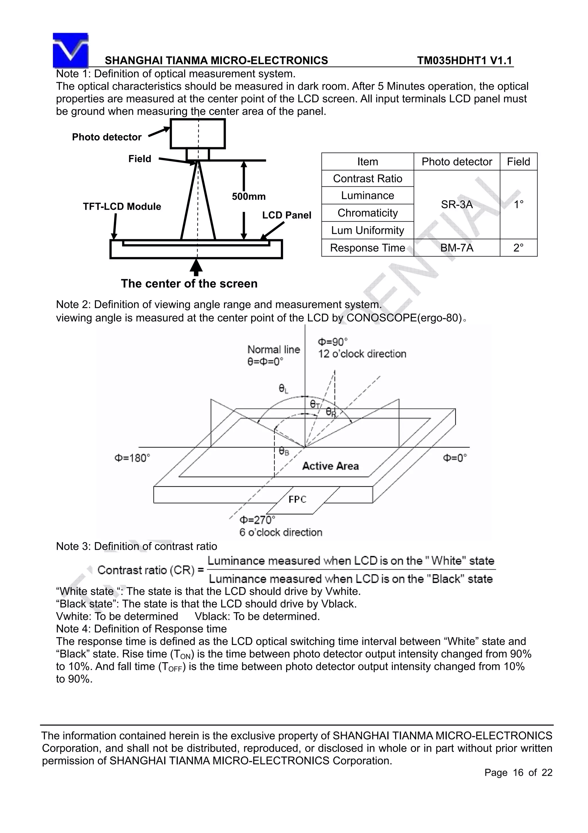
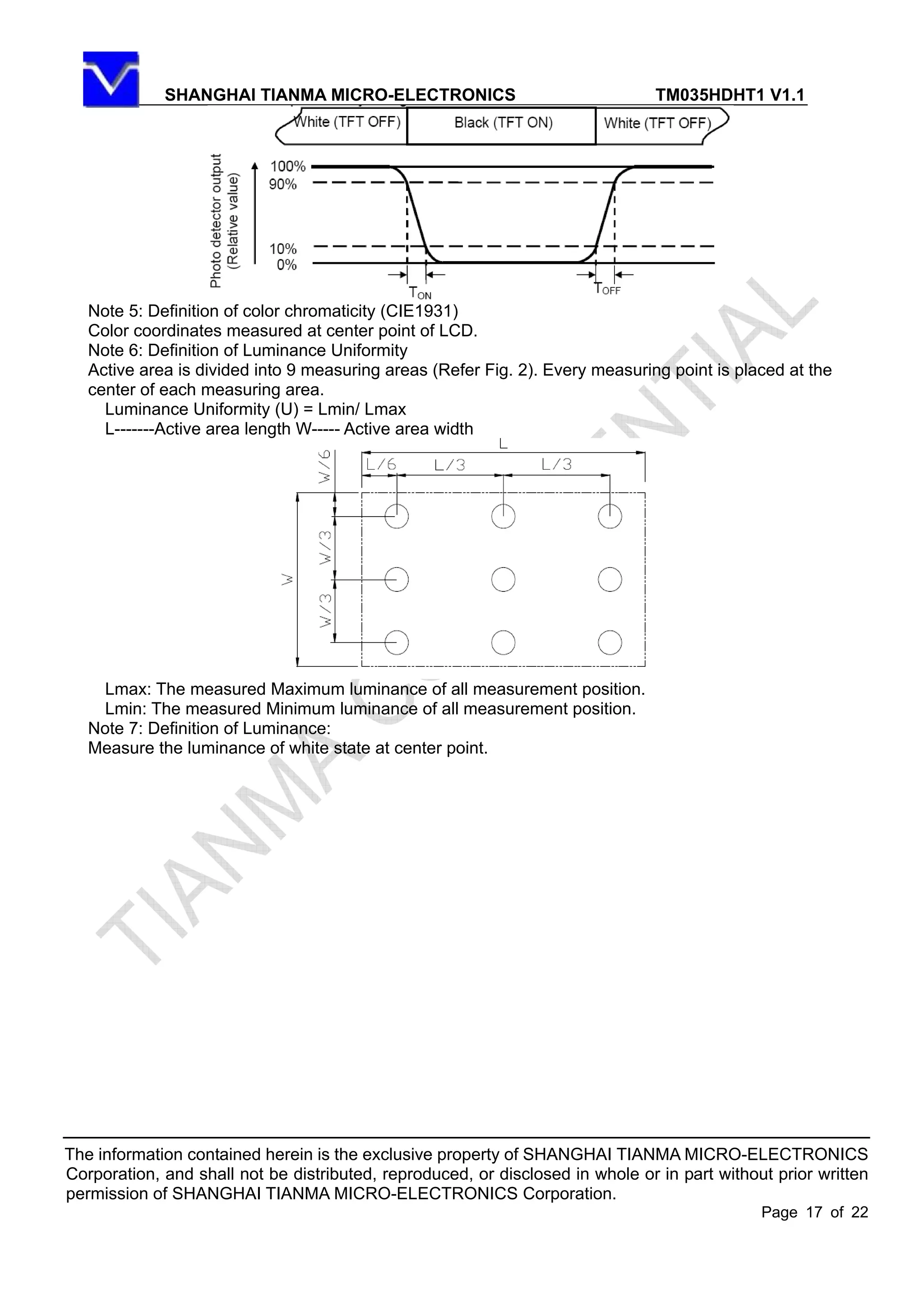
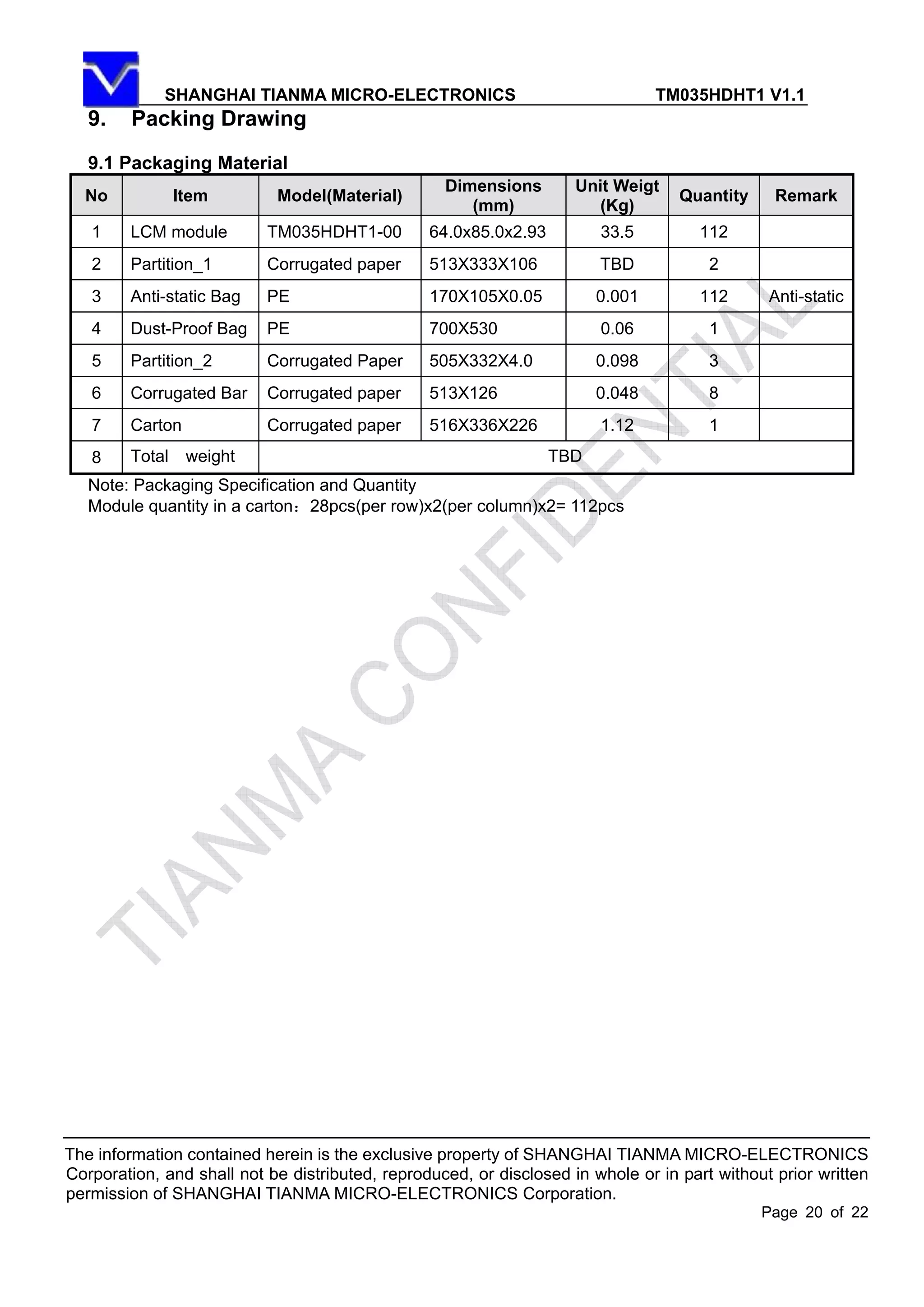
Download to read offline


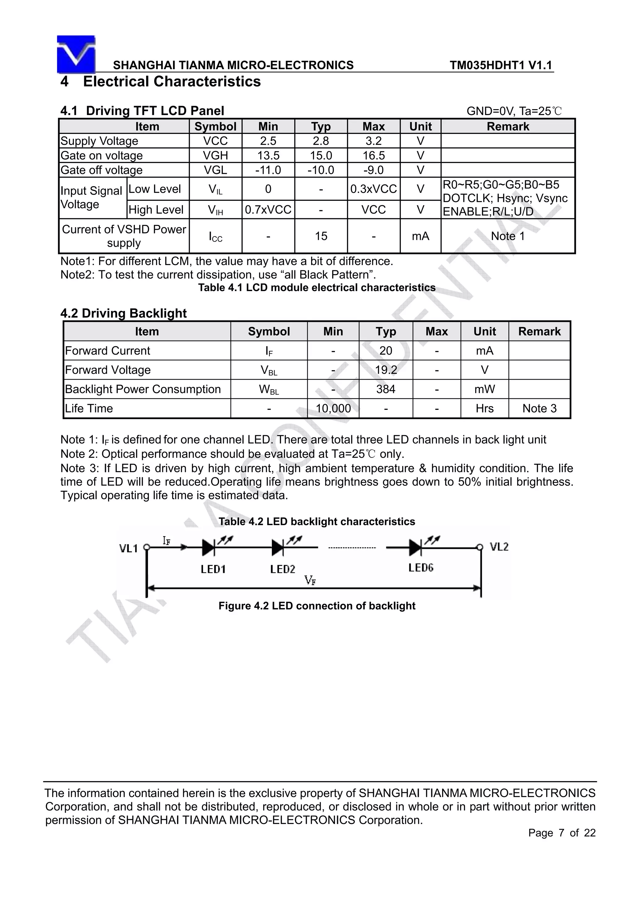
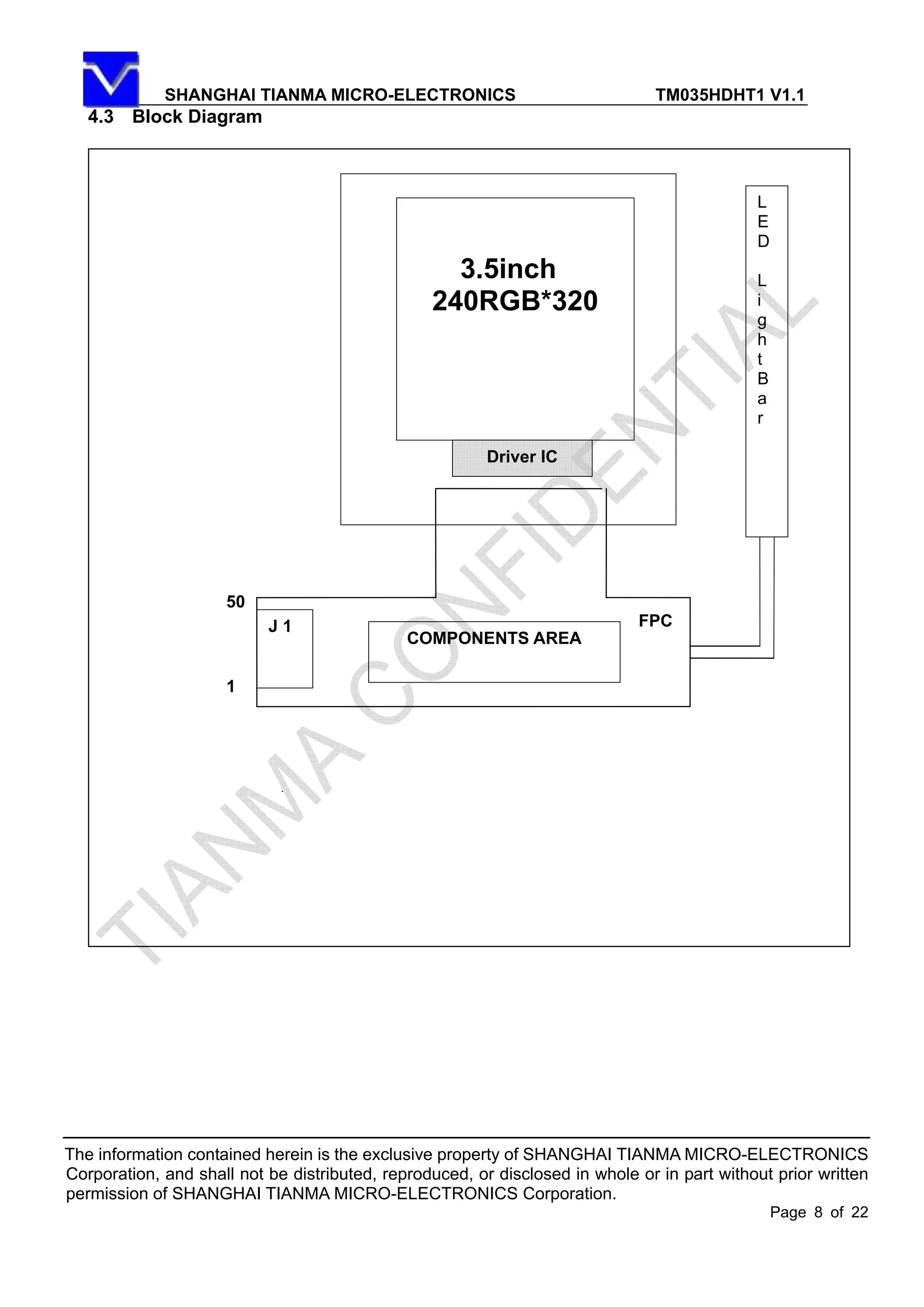


This document is a technical specification sheet for the SHANGHAI TIANMA MICRO-ELECTRONICS TM035HDHT1 V1.1 LCD module. It includes specifications for the input/output terminals, electrical characteristics when driving the TFT LCD panel and backlight, data input timing diagrams, optical characteristics, environmental tests, mechanical drawings, and precautions for use. Key specifications include a 3.5-inch TFT LCD with 240x320 RGB pixel resolution, LED backlight, and electrical characteristics for the LCD driver such as a supply voltage of 2.5-3.2V and gate voltages of 13.5-16.5V and -11 to -10V.


