1. 0
The Complete Diode Model
To understand that what the complete diode model is, following terms must
be known to us:
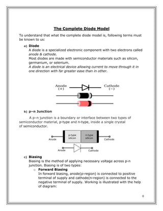
a) Diode
A diode is a specialized electronic component with two electrons called
anode & cathode.
Most diodes are made with semiconductor materials such as silicon,
germanium, or selenium.
A diode is an electrical device allowing current to move through it in
one direction with far greater ease than in other.
b) p–n Junction
A p–n junction is a boundary or interface between two types of
semiconductor material, p-type and n-type, inside a single crystal
of semiconductor.
c) Biasing
Biasing is the method of applying necessary voltage across p-n
junction. Biasing is of two types:
o Forward Biasing
In forward biasing, anode(p-region) is connected to positive
terminal of supply and cathode(n-region) is connected to the
negative terminal of supply. Working is illustrated with the help
of diagram:
2. 1
Forward bias is a close switch.
o Reverse Biasing
In reverse biasing, anode(p-region) is connected to negative
terminal of supply and cathode(n-region) is connected to the
positive terminal of supply. Working is illustrated with the help of
diagram:
Reverse Bias
Reverse bias acts as an open switch.
d) Barrier Potential
Barrier potential is the amount of energy required to produce full
conduction across the p-n junction in forward bias.
3. 2
e) Small forward Dynamic resistance
Dynamic Resistance of a p-n junction diode is the small change
in forward voltage to small change in forward current at a particular
operating point.
f) Large internal Reverse Resistance
It is the resistance which the diode offers in a circuit.
The complete model of a diode consists of the barrier potential, the small
forward dynamic resistance, and the large internal reverse resistance. The
reverse resistance is taken into account because it provides a path for the
reverse current, which is included in this diode model.
When the diode is forward-biased, it acts as a closed switch (as we already
know) in series with the barrier potential voltage and the small forward
dynamic resistance as indicated in the large internal reverse resistance as
indicated in the figure below.
When the diode is reverse-biased, it acts like a closed switch (as we already
know) in parallel with the large internal reverse resistance as shown in the
figure below. The barrier potential does not affect reverse bias; it is not a
factor.
The characteristic curve for the complete diode model is also shown in the
figure. Since the barrier potential and the forward dynamic resistance are
included, the diode is assumed to have a voltage across it when forward-
biased. This voltage consists of the barrier potential voltage plus the small
voltage drop across the dynamic resistance, as indicated by the portion of
the curve to the right of the origin. The curve slopes because the voltage
drop due to dynamic resistance increases as the current increases.
The reverse current is taken into account with the parallel resistance and is
indicated by the portion of the curve to the left of the origin. The breakdown
portion of the curve is not shown because breakdown is not a normal mode
of operation for most diodes.
4. 3
Review
g) What are the two conditions under which the diode is operated?
A diode is operated under these two conditions:
1) Forward Bias.
2) Reverse Bias.
h) Under what condition is the diode never intentionally operated?
A diode should never be operated in reverse breakdown.
i) What is the simplest way to visualize a diode?
The diode can be ideally viewed as a switch.
j) To more accurately represent a diode, what factors must be
included?
A diode includes barrier potential, dynamic resistance, and reverse
resistance in the complete model. So, the complete diode model is the
most accurate diode approximation.
k) Which diode models will be used in this book?
Complete diode model will be used in this book.