
Recommended
More Related Content
Similar to Electronics Devices and Circuits: Junction Diode Applications (39
Similar to Electronics Devices and Circuits: Junction Diode Applications (39 (20)
Recently uploaded
Recently uploaded (20)
Electronics Devices and Circuits: Junction Diode Applications (39
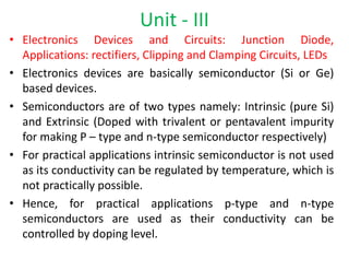
- 1. • Electronics Devices and Circuits: Junction Diode, Applications: rectifiers, Clipping and Clamping Circuits, LEDs • Electronics devices are basically semiconductor (Si or Ge) based devices. • Semiconductors are of two types namely: Intrinsic (pure Si) and Extrinsic (Doped with trivalent or pentavalent impurity for making P – type and n-type semiconductor respectively) • For practical applications intrinsic semiconductor is not used as its conductivity can be regulated by temperature, which is not practically possible. • Hence, for practical applications p-type and n-type semiconductors are used as their conductivity can be controlled by doping level. Unit - III
- 2. • Electronic circuits contain Electronic devices • Electronic devices are mostly Non-linear as the relation between voltage and current is not a straight line passing through origin. Also, they don’t follow ohm’s law • Electronic devices are mostly Unilateral as their behavior is not same if we reverse them • Electronics circuits can be categorized in two major parts viz. (a) Analog Electronics and (b) Digital Electronics • The basic building blocks of Analog electronics circuits are diode, transistor etc which in turn are used to construct logic gates and other digital electronics devices. Electronic Devices & Circuits
- 3. • Junction Diode or p-n junction diode is the simplest element of Electronics circuit. • It is fabricated by doping trivalent impurity (on half part) and pentavalent impurity (on another half part) of the single silicon wafer. • Two different pieces of silicon one with trivalent doping and another with pentavalent doping cannot be joined together to form a p-n junction diode as inter-atomic space will be much higher and electrons and holes movement will not be possible. Junction Diode
- 4. • I = Io[e^(Ve/ηkBT) - 1] • Where Io is the reverse saturation current at temperature T K • V is the applied voltage • e is electronic charge in coulomb • kB is Boltzmann constant = 1.38* 10^-23 J/K • T is temperature in K • η is a constant depending on Diode material (1 for Ge and 2 for Si) Junction Diode Current equation
- 5. • I = Io[e^(Ve/ηkBT) - 1] = Io[e^(V/ηVT) - 1] • Where VT = 0.026 V for at room temperature • This equation is valid for both forward bias as well as reverse bias • For forward bias the exponential term is much higher than unity and 1 is neglected such that the relation becomes exponential one • For reverse bias exponential term becomes negligible as compared to 1 and I is simply –IO i.e. constant value equal to reverse saturation current Junction Diode Current equation
- 6. • Piecewise Linear Diode Model: • AS per piecewise linear model Diode is treated as on/off switch in forward and reverse bias region respectively. • In reverse bias it will act as a open switch and no current flows across it. • In forward bias it will act as a close switch and a small voltage (knee voltage) drops across it. • This model is used for studying diode applications in rectifier and clipping/clamping circuits. Diode Model for applications
- 7. • Rectifier is a circuit which converts AC to DC • Rectifiers are of two types: (a) Half wave rectifier (b) Full wave rectifier • Full wave rectifiers are again of two types (i) Full wave Centre tap rectifier (ii) Full wave Bridge rectifier We will study them one by one Diode applications: Rectifiers
- 8. • The half wave rectifier rectifies only one half (either positive half or negative half) of the AC waveform to DC • In this only one diode is used. For the half cycle of the AC wave it is in the forward bias region and acts as short circuit, applying the source voltage to the load. • In the another half cycle of the AC wave it is in the reverse bias region and acts as open circuit, applying zero voltage across the load Half wave Rectifier
- 9. • Peak Inverse Voltage (PIV): Same as maximum of the transformer secondary output = Vmax • Average output voltage (Vdc): Vmax/π • RMS of output voltage (Vrms): Vmax/2 • Ripple factor (ϒ): defined as (ac component)/(dc component) = 1.21; where ac component = √((rms)^2 – (dc)^2) • Form factor: defined as ratio of rms value and dc value = π/2 = 1.57 Performance parameters for Half wave Rectifier
- 10. • In this rectifier a special type of transformer known as “Centre Tap Transformer” is used and two diodes are connected on the two extreme ends of the transformer as shown in circuit. • It is clear that in one half of the AC wave diode D1 acts as short circuit and another diode D2 acts as open circuit. In the other half of the AC wave diode D1 acts as open circuit and another diode D2 acts as short circuit. Such that a positive voltage appears always across the load. Full wave Centre Tap Rectifier
- 11. • In this rectifier a normal transformer is used and four diodes are connected in bridge like structure as shown in the circuit. • In this rectifier for one half of the AC wave diode pair D1 and D3 are forward biased and diode pair D2 and D4 are in reverse bias simultaneously such that the transformer output voltage appears across the load. • In the another half of the AC wave the earlier forward bias diode pair D1 and D3 are now reverse biased and earlier reverse biased diode pair D2 and D4 are now in forward bias such that the transformer output voltage appears across the load in the same polarity as the first half cycle. • Hence, the voltage across the load always appears in the same polarity. Full wave Bridge Rectifier
- 12. Full wave Bridge Rectifier The output of full wave bridge rectifier is same as centre-tap rectifier. But, the cost of normal transformer used here is less than the centre tap transformer. Also, the PIV ratings of the diodes used here is just half as compared to the PIV rating of diodes used for centre tap method.
- 13. • Only the PIV is different for the two types of full wave rectifiers. Rest all the parameters are same. • Peak Inverse Voltage (PIV) for Centre tap type: Twice of maximum of the transformer secondary output between one extreme and centre tap = 2Vmax • Peak Inverse Voltage (PIV) for Bridge type: Same as maximum of the transformer secondary output = Vmax • Average output voltage (Vdc): 2Vmax/π • RMS of output voltage (Vrms): Vmax/√2 • Ripple factor (ϒ): defined as (ac component)/(dc component) = 0.482; where ac component = √((rms)^2 – (dc)^2) • Form factor: defined as ratio of rms value and dc value = π/2√2 = 1. 11 Performance parameters for Full wave Rectifier
- 14. • The clipper circuit is a circuit which clips (removes) some portion of the applied waveform • Clipping circuits are widely used in RADAR, digital and other electronic systems. • Simple clipping circuits can be configured using diodes • The important types of clipping circuits are as follows: 1. Positive clipper: removes positive half of waveform 2. Negative clipper: removes negative half of waveform 3. Biased clipper: removes some portion of positive or negative half (not completely the half portion) 4. Combination clipper: removes some part of positive half as well as some part of negative half simultaneously Diode applications: Clippers
- 15. Positive Clipper As explained earlier the Positive Clipper removes the positive half of waveform completely and only the negative half of the waveform is available in the output as shown in the figure.
- 16. Negative Clipper As explained earlier the Negative Clipper removes the negative half of waveform completely and only the positive half of the waveform is available in the output as shown in the figure.
- 17. Biased Clipper The biased Clipper has a DC source in series with the Diode such that the DC source will reverse bias the diode as shown in the figure. Till the time AC voltage is lower than the DC source, the diode will remain reverse biased and source voltage will appear across the load. Once the AC source voltage is higher than the DC source the diode will be forward biased (short) such that the DC source voltage will appear across the load as shown in the figure.
- 18. Combination Clipper The combination Clipper will have two parallel branches in which diode will be connected in opposite direction and two different DC sources will be connected in series with the Diodes as shown in the figure. In positive half cycle till the time AC voltage is lower than the DC source V1, the diode D1 will remain reverse biased and source voltage will appear across the load. Similarly, in negative half cycle till the time AC voltage is lower than the DC source V2, the diode D2 will remain reverse biased and source voltage will appear across the load. Once the AC source voltage is higher than the DC source (either V1 or V2) the corresponding diode will be forward biased (short) such that the DC source voltage will appear across the load as shown in the figure.
- 19. • A clamper circuit is a circuit which introduces a DC level to an applied AC signal. • The effect of the clamper circuit is that the whole input waveform clamps (shifts) up or down without any change in the waveform. • For constructing a clamper circuit, a capacitor of high capacitance is chosen such that the time constant of the RC circuit is high as compared to the time period of applied voltage such that it will be assumed that capacitor will maintain a fairly constant voltage once charged. • The clamper circuits are of two types: 1. Positive peak clamper or clamp down circuit or Negative DC restoring circuit 2. Negative peak clamper or clamp up circuit or Positive DC restoring circuit Diode Clamper
- 20. Positive peak clamper or clamp down circuit or Negative DC restoring circuit As discussed earlier, for constructing a clamper circuit, a capacitor of high capacitance is chosen such that the time constant of the RC circuit is high as compared to the time period of applied voltage such that it will be assumed that capacitor will maintain a fairly constant voltage once charged. The circuit diagram and output of the clamp down clamper is as shown in the figure below.
- 21. Negative peak clamper or clamp up circuit or Positive DC restoring circuit As discussed earlier, for constructing a clamper circuit, a capacitor of high capacitance is chosen such that the time constant of the RC circuit is high as compared to the time period of applied voltage such that it will be assumed that capacitor will maintain a fairly constant voltage once charged. The circuit diagram and output of the clamp up clamper is as shown in the figure below.
- 22. • LEDs are special purpose diodes, which emit light when connected in forward bias. • They are fabricated of different materials (like GaAs, GaP, GaAsP etc) for emitting different color light. • These materials have band gap energy (between Valence and Conduction band) in the range of 1.5 – 3 eV, and emits radiation of visible range by the recombination of electrons and holes • The use of LEDs as a light source is increasing very fastly now a days as they are more efficient than tungsten filament bulb as the energy is not converted to heat in them. Light emitting Diodes (LEDs)