intel microprocessors manufacturing and generations
•Download as PPTX, PDF•
0 likes•46 views

intel

Recommended
Recommended
More Related Content
What's hot
What's hot (20)
Similar to intel microprocessors manufacturing and generations
Similar to intel microprocessors manufacturing and generations (20)
Recently uploaded
Recently uploaded (20)
intel microprocessors manufacturing and generations
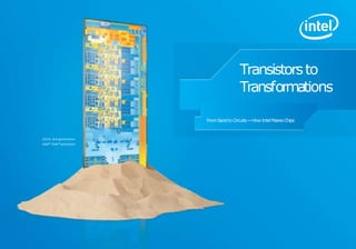
- 1. 22nm 3rd generation Intel® Core™ processor Transistorsto Transformations FromSandto Circuits—How Intel MakesChips
- 2. “For years we have seen limits to how small transistor can get this change in the basic structure is a truly revolutionary approach,
- 3. And one that should allow MOORE’S law and the historic pace of innovation to be continued” - Gordan E Moore , cofounder, intel corporation .,
- 4. REVOLUTIONARY For decades, Intel’s research anddevelopment, advanced silicon chips, and manufacturing have brought together the best of computing, communications, and consumer electronics to enable valuable benefits fromtechnology. Intel continues to introduce new process technologies that deliver more energy-efficient, secure, and higher-performance products, which are then designed into your increasinglyconnected, smarterdevices. MOORE’S LAW According to Moore’s Law, the number of transistors on achip roughly doubles every couple of years. As aresult, the transistor scale gets smaller and smaller. As the transistor count climbs, so does the ability to integrate more capabilities onto achip and increase device complexity. The cumulative impact of these spiralingincreases in capabilities enables today’s mobile devices, fuels the increasingly Internet-connected and information-rich digital experiences weseek, and powers industries and our globaleconomy. Delivering Moore’s Law requires numerous innovations. Intel’s world-first, advanced transistor design introductionsinclude strained silicon (2003), 45nmwith high-k/metal gate silicon technology (2007),followed by the 32nm2ndgeneration high-k/metal gate silicon technology (2009). Recently, Intel introduced another radical design change—22nm3-D Tri-Gate transistors (2011), which entered high-volume productionin 2012. YOUR WORLD CONNECTED “Our vision is very simple:if it consumes electricity, it’s going to end up computing,and if it’s computing, it will be connected to the Internet,” stated Kirk B. Skaugen,Intel Vice President and General Manager of the PCClient Group.He was describing server cloud computing capabilities and connected device growth expected within the next decade at the Web2.0 Summitin November2011. 1 Forecasts call for 15 billion connected devices and 2 over three billion connected users by 2015.The growthofglobaldatathrough2015isexpectedto 3 surpass4.8zettabytes peryear. Attheselevels, eachconnected user will generate morethan four GB ofdatatrafficeveryday.That’s the equivalent of a4-hour HDmovie. THE POWER TO TRANSFORM From Ultrabook™ devices, datacenters, and high performance computing, to applications, security, and Intel-powered smartphones and tablets, the only thing more amazingthan Intel’s technology is whatyoudowithit. Find definitions of italicized words in the “Terminology” sectionat the end of this brochure. A SmartWorld
- 5. 2008* Intel® Core™2 Duo processor die 45nmhigh-k/metalgate silicontechnology) 2010* 2nd generation Intel® Core™ processor die (32nmprocesstechnology) 2012* 3rd generation Intel® Core™ processor die (manufactured onindustry-leading 22nmprocess technology with 3-DTri-Gatetransistors) Die not shown to scale. *Date of high volumeproduction 20155th generation intel core processor die (14nm process technology) 20177th generation intel core processor die (4.2GHz clock speed)
- 6. ADVANCED DESIGN Intel creates industry-leading and world-first silicon products that introduce more capabilities, are smaller,more powerful, and use less energy. While advancing technology, Intel incorporates environmental principles into each step of the productlife cycle. Andby anticipatingthe needs for the next generation, Intel’s success at advanced chip design has helped drive other innovations in almost allindustries. WHAT IS A CHIP? A chip, also known as adie or processor, is a microelectronic device that can process information in the form of electrical current traveling along a circuit. Although they look flat, today’s chips may have more than 30 layers of complex circuitry compared to five layers on the 4004, Intel’s first processor, introduced in1971. HOW CHIPS WORK The way achip works is aresult of how achip’s transistors and gates are designed and the use ofthe chip. A chip can contain millions or billions of transistors interconnected in acertain manner.These transistors act as switches, either preventing or allowing electrical current to pass through. A gate turns the transistors on and off, allowing electrical currents to send, receive, and process digital data(1sand 0s)as instructions and information.Chips today can have multiplecores. THE ULTIMATE PUZZLE How would you organize something with 1,000,000,000 pieces, and then create aplan so it can be put together correctly and on time? Worldwide teamwork is critical. Precision counts. Rules matter.Many types of engineerswork closely together to design chips and translate circuit schematics into mask layers formanufacturing. Before Intel makeschips, engineers ensure the accuracy of the specification. They begin with a design or blueprint and consider manyfactors: What type of chip is needed and why? How many transistors can be built on the chip? What is the optimal chip size? What technology will beavailable to createthe chip? When does the chip need to be ready? Where will it be manufactured and tested? To answer these questions, Intel teams work with customers, software companies, and Intel’s marketing, manufacturing, and testing staff. The design teamstake this input and begin the monumental task of defining achip’sfeatures anddesign. Whenthe specifications for the chip areready, Intel creates alogic design, an abstract representation of the hundreds of millions of transistors and interconnections that control the flow ofelectricity through achip. After this phase is complete, designers prepare physical representationsof each layer of the chip and its transistors. They then develop stencil-like patterns, or masks, for each layer of the chip that are used with ultraviolet (UV)light during afabrication process called photolithography. To complete the design, testing, and simulation of achip, Intel uses computer-aided design (CAD) tools. CADhelps designers create very complex designs that meet functional, performance, and power goals.After extensive modeling, simulation, and verification, the chip is ready forfabrication. It can take hundreds of engineersworking multiple years to design, test, and ready anew chip design forfabrication.
- 8. Global.Connected. MissionCritical. FABRICATION The process of makingchips is called fabrication. Inside Intel’s ultra-clean fabs, the world’s most complex, tiniest machines —processors and other silicon chips —are built in asustainable manner. Intel fabs are amongthemost technically advanced manufacturing facilities in the world. Within these sophisticated fabs, Intel makeschips in aspecial area called acleanroom. Because particles of dust can ruin the complex circuitry on achip, cleanroom air must be ultra- clean. Purified air is constantly recirculated, entering through the ceiling and exiting through floor tiles. Technicians put on aspecial suit, commonly called abunny suit, before they entera cleanroom. This helps keep contaminants such as lint and hair off the wafers. Inacleanroom, acubic foot of air contains lessthan one particle measuring about 0.5 micron (millionth of ameter) across. That’s thousands of times cleaner than ahospital operatingroom. Automation has acritical role in afab. Batches of wafers are kept clean and are processed quickly and efficiently by traveling through the fab inside front-opening unified pods (FOUPs) on an overhead monorail. Each FOUP receives abarcode tag that identifies the recipe that will be used to makethe chips inside. This labeling ensures the correct processing at each step of fabrication.Each FOUP contains up to 25 wafers and weighs more than 25 pounds. Production automationmachinery allows for this FOUP weight, which is too heavy to be handled manually bytechnicians. Above: 3rd generation Intel®Core™wafer Intel’smanufacturingleadershipincludesaglobalnetworkof high-volume, technicallyadvancedwaferfabricationfacilities,orfabs,thatrun24hours aday,7 daysaweek,365daysayear.
- 9. Top left:OrangeFOUPscarry300mmwafersin anautomated fab. Top right: Highly-trained technicians monitor eachphaseofchip fabrication. Bottom left: Purified air enters from the ceiling and exits through perforated floor tiles. Bottom right:The 32nmplanartransistor(onleft) illustratescurrent(representedbyyellow dots) flowing in a flat plane under the gate, while Intel’s smaller 22nm 3-D Tri-Gatetransistor (onright) illustrates increased current flow over three sides of a vertical fin.
- 10. SAND TO INGOT Sand Sandhas ahigh percentage of silicon—the starting material forcomputer chips. Silicon is a semiconductor,meaning that it can be turned into an excellent conductor or insulator of electricity with minor amounts of impuritiesadded. Melted Silicon Silicon is purified to less than one alien atom per billion. It is melted and cooled into a solid crystal lattice cylinder, called aningot. Monocrystalline Silicon Ingot The silicon ingot has adiameterof 300 millimeters (mm)and weighs about 100 kilograms(kg). PHOTOLITHOGRAPHY Applying Photoresist Photolithography is aprocess that imprints a specific pattern on the wafer.It starts by applying alight-sensitive, etch-resistant materialcalled photoresist onto the wafersurface. Exposing Photoresist The photoresist is hardened and parts of it are exposed to ultraviolet light, makingit soluble. The light passes through amask(similar to astencil), and then through alens to shrink and print circuit patterns on each layer of every chip on the wafer. Developing Resist A chemical process removes the soluble photoresist, leaving apatterned photoresist imageas determinedby what was on themask. INGOT TO WAFER Slicing Ingots The ingotis cut into individual silicon discs called wafers. Each wafer is about onemmthick. Polishing Wafers The wafers are polished to aflawless, mirror-smooth surface. Intel buysthese manufacturing-readywafers. HowIntelMakesChips
- 11. ION IMPLANTATION Implanting Ions Ions(positively or negatively charged atoms) are embedded beneath the surface of the wafer in regions not covered by photoresist. This alters the conductive properties of the silicon in selectedlocations. Removing Photoresist After the ion implantation, the photoresist is removed, resulting in certain regions beingdoped with alien atoms(green in theimage). The Transistor Although hundreds of chips are usually built on a single wafer,the next steps focus on asmall piece of achip—atransistor. TEMPORARY GATE FORMATION Creating a Gate Dielectric Photoresist is appliedto portions of the transistor, and athin silicon dioxide layer (red in the image)is created by inserting the wafer in an oxygen-filled tube-furnace. This layer becomes atemporarygate dielectric. Creating a Gate Electrode Using photolithography, atemporary layer of polycrystalline silicon (yellow in the image)is created.This becomes atemporary gateelectrode. Insulating the Transistor Inanother oxidation step, asilicon dioxide layer is created over the entire wafer (transparent red in the image)to insulate the transistor from otherelements. ETCHING Etching To create afin for atri-gate transistor, Intel applies ahard maskmaterial(blue in the image)using photolithography.Then achemical is appliedtoetch away unwanted silicon, leaving behind afin with a layer of hard maskontop. Removing Hard Mask The hard maskis chemically removed, leaving a tall, thin siliconfin that will contain the channel of atransistor. CHIPS ARE THREE-DIMENSIONAL STRUCTURES built simultaneously on batches of wafers in a fab. Making chips is a complex processrequiring hundreds of precisely controlled steps that result in patterned layers ofvarious materials built one on top of another. These layers form the circuits, which include electrical pathways and transistors (switches). Follow some of the keysteps illustrating Intel’s chipmanufacturing process for the 22nm 3rd generation Intel® Core™processors.
- 12. “GATE-LAST” HIGH-K/METAL GATE FORMATION Removing the Temporary Gate The temporary gate electrode and gatedielectric are etched away in preparation for forming the final gate.This procedure is called gate-last. Applying High-k Dielectric Material Multiple layers of high-k dielectric material (yellow in the image)are applied to the wafer surface using amethodcalled atomic layer deposition. This materialis etchedawayin some areas, such as the silicon dioxidelayer. Forming a MetalGate A metal gate electrode (blue in the image)is formed over the wafer and removed fromregions other than the gate electrode. The combination of this and the high-k dielectric materialimproves performance and reducesleakage. METAL LAYERS Polishing The excess materialis polished off, revealing aspecific pattern ofcopper. Connecting with Metal Layers Like amulti-level highway, metal layers interconnect the transistors in achip (middleand right images).The designof the chip determines how the connections are made.Although chips look flat, they can have more than 30 layersof this complexcircuitry. METAL DEPOSITION Preparing to Connect the Transistor Three holes are etched into the insulation layer (red in the image)above the transistor. Theholes are filled with copper or another materialthat creates metal connections to othertransistors. Electroplating The wafers are put into a copper sulphate solution. Copper ions are deposited onto the transistor using aprocess calledelectroplating. After Electroplating Copperions settle as athin layer of copperon the transistorsurface. HowIntelMakesChips
- 13. WAFER SORT TEST AND SINGULATION Sort Testing Afterwafer processing is complete,each chip on awafer is testedfor its functionality. Slicing Wafers The wafer is cut into pieces called die. Moving to Packaging Based on the responses received in the wafer sort test, die are selected for packaging. CLASS TESTING AND COMPLETED PROCESSOR Package Testing Processors undergo final testing for functionality, performance, andpower. Binning Based on final test results, processors with the same capabilities are grouped into transporting trays. Retail Packaging Intel®processors, such as the 3rd generation Intel Core processor shown here, are sent to system manufacturers in trays, or they are boxed for retailstores. PACKAGING DIE Individual Die The silicondie shown here is a3rd generationIntel® Core™processor, Intel’s first 22nm microprocessor using 3-Dtransistors. Packaging The substrate, the die, and aheat spreader are put together to form acompleted processor. Thegreen substrate creates the electrical and mechanical connections so that the processor can interact with the system. The silver-colored heat spreader is athermalinterface that helps dissipateheat. Completed Processor A completed processor, such as the 3rdgeneration Intel Core processor, is one of the most complex manufactured products onEarth.
- 14. Intel® 4004 processor Initial clock speed:108KHz Transistors: 2,300 Manufacturingtechnology: 10micron Intel® 8008 processor Initial clock speed:800KHz Transistors: 3,500 Manufacturingtechnology: 10micron Intel® 8080 processor Initial clock speed:2MHz Transistors: 4,500 Manufacturingtechnology: 6micron Intel® 8086 processor Initial clock speed:5MHz Transistors: 29,000 Manufacturingtechnology: 3micron Intel® 286 processor Initial clock speed:6MHz Transistors: 134,000 Manufacturingtechnology: 1.5micron Throughout Intel’shistory,newandimprovedtechnologies have transformed the human experience. 1971 IntelChips 1972 1974 1978 1982 1985 1989 1993 1995 Intel386™ processor Initial clock speed:16MHz Transistors: 275,000 Manufacturingtechnology: 1.5micron Intel486™ processor Initial clock speed:25MHz Transistors: 1.2million Manufacturingtechnology: 1micron Intel® Pentium® Pro processor Initial clock speed:200MHz Transistors: 5.5million Manufacturingtechnology: 0.35micron Intel® Pentium® processor Initial clock speed:66MHz Transistors: 3.1million Manufacturingtechnology: 0.8micron
- 15. Decades of Intel chips, including the 22nm 3rd generation Intel®Core™processor with its revolutionary 3-D Tri-Gate transistors, illustrate Intel’s unwavering commitment to delivering technology and manu- facturing leadership to thedevices you use every day.As you advance throughthe chart, the benefits of Moore’s Law, which states that the number of transistors roughly doubles every couple of years, are evident as Intel increases transistor density and innovates the architecture designs that deliver more complex, powerful, and energy-efficient chips that transform the way we work, live, and play. Intel® Pentium® Mprocessor Initial clock speed:1.7GHz Transistors: 55 million Manufacturing technology: 90nm Intel® Core™2 Duo processor Initial clock speed:2.66GHz Transistors: 291 million Manufacturing technology: 65nm Intel® Core™2 Duo processor Initial clock speed:2.4GHz Transistors: 410million Manufacturing technology: 45nm Intel® Atom™ processor Initial clock speed:1.86GHz Transistors: 47 million Manufacturingtechnology: 45nm 2nd generation Intel® Core™ processor Initial clock speed:3.8GHz Transistors: 1.16billion Manufacturingtechnology: 32nm 3rd generation Intel® Core™ processor Initial clock speed:2.9GHz Transistors: 1.4billion Manufacturingtechnology: 22nm 2003 2006 2008 2008 20122010 1997 1998 1999 2000 2001 Intel® Pentium® processor Initial clock speed:300MHz Transistors: 7.5million Manufacturingtechnology: 0.25micron Intel® Celeron® processor Initial clock speed:266MHz Transistors: 7.5million Manufacturingtechnology: 0.25micron Intel® Pentium® III processor Initial clock speed:600MHz Transistors: 9.5million Manufacturingtechnology: 0.25micron Intel® Pentium® 4 processor Initial clock speed:1.5GHz Transistors: 42 million Manufacturingtechnology: 0.18micron Intel® Xeon® processor Initial clock speed:1.7GHz Transistors: 42 million Manufacturingtechnology: 0.18micron
- 16. 2013 4thgeneration Intel core processor Initial clock speed:3.80GHz Transistors :1.4 billion Manufacturing technology: 22nm 2015 5thgeneration Intel core processor Initial clock speed:3.80GHz Transistors:1.9 billion Manufacturing technology: 14nm 2016 6thgeneration Intel core processor Initial clock speed:3.80GHz Transistors:2.27 billion Manufacturing technology: 14nm 2017 7th generation Intel core processor Initial clock speed :4.2GHz Transistor:2.27 billion Manufacturing technology: 14nm
- 17. NEW LEVELS OF SECURITY The full benefits of technologycan only be realized when the computing experience is secure—when individuals can be certain that personalinformation remains personal, and when businesses can ensure that data and systems integrity isnever breached. To enable this vision, Intel is delivering anew level of security that builds protection and safety into the heart of computing technology. From silicon,to software, to services, Intel is building security into everything wedo. Oneexample isthe Ultrabook, which delivers asafer experience with security technology features built into the chip.Intel®Anti-Theft6 and Intel®Identity Protection7 technologies, coupled with software and services, protect your identity and data for greater peace-of-mind. THE ULTIMATE MOBILE DEVICE Intel Capitalis investing to help accelerate innovation and the adoption ofnew technology and services in the automotiveindustry. The funding is part of Intel’s ongoing work with automakers and in-vehicle infotainment suppliers to help integrate advanced technologies into cars. Ultimately,the connected car will have the intelligenceand context awareness to offer the right information,at the right time, and in the right way to keep drivers and passengers informed, entertained, and productive while maintaining optimal safety. Aconnected car could then communicate with the cloud, the transportation infrastructure, and even other vehicles to provide additional services such as advanced driver assistance and real-timetraffic informationto optimizethe flow of traffic. THE HEART OF INNOVATION Throughout Intel’s history, we have pushedthe boundaries of what’s possible. Our vision for the next decade is evenmore ambitious. Intel believes that education, innovation, and entrepreneurship are the keys todriving economic growth and improving social conditions. Skills such as digital literacy, problemsolving, criticalthinking, and collaboration are best developedin active learning environments supported by technology to inspire the nextgeneration. This Next Decade Intelwillcreate and extend computing technology to connect and enrichthe lives of everypersononEarth.Webelieve fundamentallythat computing technology will haveapositive impactoneveryindividual,business,and communityaroundtheworld.
- 18. Thankyou.,