1. Kumar Suryanshu (2K20/VLS/08)
Experiment No. 03(a)
Aim:-
i).To implement dynamic latch and calculate its set up time, hold time, c to q delay ,d to q delay
for different value of capacitance.
ii). To implement a Dynamic Transmission Gate Edge Triggered D Flip-Flop calculate its set-
up time, hold time, clk-Q delay, D-Q delay.
Theory:-
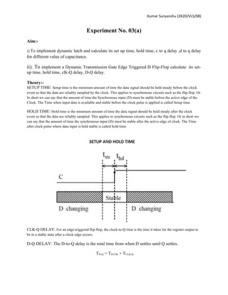
SETUP TIME: Setup time is the minimum amount of time the data signal should be held steady before the clock
event so that the data are reliably sampled by the clock. This applies to synchronous circuits such as the flip-flop. Or
In short we can say that the amount of time the Synchronous input (D) must be stable before the active edge of the
Clock. The Time when input data is available and stable before the clock pulse is applied is called Setup time.
HOLD TIME: Hold time is the minimum amount of time the data signal should be held steady after the clock
event so that the data are reliably sampled. This applies to synchronous circuits such as the flip-flop. Or in short we
can say that the amount of time the synchronous input (D) must be stable after the active edge of clock. The Time
after clock pulse where data input is held stable is called hold time.
CLK-Q DELAY: For an edge-triggered flip-flop, the clock-to-Q time is the time it takes for the register output to
be in a stable state after a clock edge occurs.
D-Q DELAY: The D-to-Q delay is the total time from when D settles until Q settles.
TD-Q = TD-ClK + TCLK-Q
2. Kumar Suryanshu (2K20/VLS/08)
For analysis of setup time, hold time, clk-Q delay, we implement Dynamic Transmission Gate
Edge Triggered D Flip-Flop using master-slave concept. We use NMOS (L=180nm, W=360nm)
and PMOS (L=180nm, W=720nm) with 180nm technology file.
Observations:-
Figure3.1: Circuit diagram of dynamic latch using transmission gate
3. Kumar Suryanshu (2K20/VLS/08)
i). Observation for C=100f capacitance value
Figure 3.2: Transient response of the Dynamic latch
Figure 3.3: Transient response of the Dynamic latch when setup and hold violation occurred
8. Kumar Suryanshu (2K20/VLS/08)
Figure 3.12: Transient response for different values of capacitance of the Dynamic latch
ii). Observation for C=10f value of capacitance
Figure 3.13: Setup time and Hold time violation for the Dynamic latch
13. Kumar Suryanshu (2K20/VLS/08)
iii). Observation For Dynamic negative edge triggered D Flip Flop
Figure 3.23: Transient response for the Dynamic negative edge triggered D Flip Flop
Figure 3.24: Setup and Hold time violation for Dynamic edge negative triggered D Flip Flop
14. Kumar Suryanshu (2K20/VLS/08)
Figure 3.25: Setup Time for the dynamic negative edge triggered D FF
Figure 3.26: Setup Time for the dynamic negative edge triggered D FF
15. Kumar Suryanshu (2K20/VLS/08)
Figure 3.28: Clock to Q delay for the dynamic negative edge triggered D FF
Figure 3.29: Clock to Q delay for the dynamic negative edge triggered D FF
Calcula on:
For Dynamic latch:
Capacitor value Tsetup Thold Tclk-Q TD-ClK TD-Q= TD-ClK + TCLK-
Q
100f 1.1ns 0.65ns 0.56ns 0.37ns 0.83ns
10f 0.482ns 0.567ns 0.4857ns 0.323ns 0.809ns
16. Kumar Suryanshu (2K20/VLS/08)
For dynamic negative edge triggered D FF:
Tsetup = 0.81ns
Thold = 0 ns
Tclk-Q= 0.296ns
TD-ClK = 0.81ns
TD-Q = 1.106ns
Result & Conclusion:
1. We have calculated Setup time , Hold time, D- Clk delay, Clk-Q delay and D-Q delay for Dynamic Latch
and dynamic negative edge triggered D FF
2. As we increase the capacitors values the setup time, clk-Q delay and D-Q delay increases.