SlideShare a Scribd company logo
1 of 20
Download to read offline
EverDisplay Optronics (Shanghai) Limited
Confidential Level3
Page:1/20
Product Specification
Doc No:
Ver No:01
The copyright belongs to EDO, Any unauthorized use is prohibited
AMOLED
Product Specification
Model Name: E1473AC63.B
Description: 1.47”
Doc. Version: 01
Customer: XM
■Approved for Preliminary Specification
□Approved for Final Specification
□Approved for Final Specification & Sample
Prepared Checked Approved
陈晟
Customer’s Approval
M
o
r
e
D
i
s
p
l
a
y
P
a
n
e
l
s
O
n
w
w
w
.
p
a
n
o
x
d
i
s
p
l
a
y
.
c
o
m
EverDisplay Optronics (Shanghai) Limited
Confidential Level3
Page:2/20
Product Specification
Doc No:
Ver No:01
The copyright belongs to EDO, Any unauthorized use is prohibited
Version History
Version. No Date Contents Remark
01 2020.04.20 First Draft
M
o
r
e
D
i
s
p
l
a
y
P
a
n
e
l
s
O
n
w
w
w
.
p
a
n
o
x
d
i
s
p
l
a
y
.
c
o
m
EverDisplay Optronics (Shanghai) Limited
Confidential Level3
Page:3/20
Product Specification
Doc No:
Ver No:01
The copyright belongs to EDO, Any unauthorized use is prohibited
Contents
1 Scope.......................................................................................................................................................... 4
2 Features...................................................................................................................................................... 4
2.1 Product Applications ............................................................................................................................ 4
2.2 Product Features................................................................................................................................... 4
3 Mechanical Specifications ......................................................................................................................... 4
4 Maximum Rating ....................................................................................................................................... 4
5 Electrical Specifications............................................................................................................................. 5
5.1 Electrical Characteristics...................................................................................................................... 5
5.2 TP IC Recommended Operating Conditions ........................................................................................ 5
5.3 I/O Connection ................................................................................................................................... 10
5.4 Graphic memory writing direction ..................................................................................................... 11
5.5 Recommended Operating Sequence................................................................................................... 11
6 Electro-Optical Specification................................................................................................................... 14
7 Reliability................................................................................................................................................. 14
7.1 Environmental Test............................................................................................................................. 17
7.2 Electrical Test ..................................................................................................................................... 17
7.3 Mechanical Test.................................................................................................................................. 18
8 Outline Dimension Drawing.................................................................................................................... 19
9 Packing Specification................................................................................................................................ 20
10 The Control of Hazardous Substances...................................................................................................... 20
M
o
r
e
D
i
s
p
l
a
y
P
a
n
e
l
s
O
n
w
w
w
.
p
a
n
o
x
d
i
s
p
l
a
y
.
c
o
m
EverDisplay Optronics (Shanghai) Limited
Confidential Level3
Page:4/20
Product Specification
Doc No:
Ver No:01
The copyright belongs to EDO, Any unauthorized use is prohibited
1 Scope
This Specification defines AMOLED manufactured by EverDisplay Optronics(Shanghai)
Limited, from here on refer as EDO. In the case of any unspecified item, it may require both
EDO and the party designs this module into its product to work out a solution.
2 Features
2.1 Product Applications
Display/Touch terminals for Smart Watch
2.2 Product Features
1) Display color:16.7M (RGB x 24bits)
2) Display format:1.47”(194 RGB*368)
3) Pixel arrangement:Real RGB arrangement
4) Interface:Quad SPI
5) Driver IC: SH8501B (COF)
6) On cell touch sensor
7) Pixel format:only support 16bit GBRG 3553
3 Mechanical Specifications
Item Specification unit
LTPS Glass outline 19.36(V) x 36.17(W) mm
Encapsulation Glass outline 19.36(V) x 35.42(W) mm
Number of dots 194(W) x RGB x 368(H) dots
Active area 17.46*33.12 mm
Diagonal size 1.47 inch
Pixel pitch 90*90 μm
Glass thickness
(LTPS/Encap. Glass/POL)
0.2/0.3/0.147 mm
Weight TBD g
4 Maximum Rating
Parameter Symbol
Spec
Unit Note
Min. Typ. Max.
Analog/boost power voltage VCI 3.2 3.3 3.4 V -
I/O voltage VDDIO 1.7 1.8 1.9 V -
M
o
r
e
D
i
s
p
l
a
y
P
a
n
e
l
s
O
n
w
w
w
.
p
a
n
o
x
d
i
s
p
l
a
y
.
c
o
m
EverDisplay Optronics (Shanghai) Limited
Confidential Level3
Page:5/20
Product Specification
Doc No:
Ver No:01
The copyright belongs to EDO, Any unauthorized use is prohibited
Operating temperature Top -20 - 70 ℃ -
Storage temperature Tstg -30 - 80 ℃ -
5 Electrical Specifications
5.1 Electrical Characteristics
5.1.1 Power Characteristic:
Item Symbol Min. Typ. Max. Unit Remark
AMOLED Power positive ELVDD 3.2 3.3 3.4 V -
AMOLED power Negative ELVSS -3.4 -3.3 -3.2 V Ref
Digital Power supply VDDIO 1.7 1.8 1.9 V Ref
Analog Power supply VCI 3.2 3.3 3.4 V Ref
1) Normal Mode
Power Supply: VDDIO =1.8V VCI=3.3V ELVDD=3.3V,ELVSS=-3.3V
Frame Frequency: Fframe =60HZ @ 25degC, Brightness 450 nits,
Display Condition Symbol Min. Typ. Max. Unit Remark
100% Pixel On,450nits
Normal
mode
- 110 130 mW Ref
2) Idle Mode
Power Supply: VDDIO=1.8V VCI=3.3
Frame Frequency: Fframe =15HZ @ 25degC, Brightness 50 nits,
Display Condition Symbol Min. Typ. Max. Unit Remark
10% Pixel On,50nits Idle mode - 6.5 8.2 mW Ref
3) Deep Standby Mode
Display Condition Symbol Min. Typ. Max. Unit Remark
All Pixel Off,0nits/ Vci
off/Vddio on
Standby
mode
- - 50 μW -
5.2 Driver IC
SH8501B (refer to the datasheet)
5.3 TP IC
ZTW622
M
o
r
e
D
i
s
p
l
a
y
P
a
n
e
l
s
O
n
w
w
w
.
p
a
n
o
x
d
i
s
p
l
a
y
.
c
o
m
EverDisplay Optronics (Shanghai) Limited
Confidential Level3
Page:6/20
Product Specification
Doc No:
Ver No:01
The copyright belongs to EDO, Any unauthorized use is prohibited
5.3.1 Basic Specifications
No. Item Specification Description Remark
1 Project ID 10 Bytes
1.The ninth byte
increased by 1 if
sensor or circuit
changed and cannot
use one TP FW
compatible for them.
2.No need to read it
by FW
2
Communication Protocol to
Host
I2C
3 I2C Address TBD
4 Touch Origination Dot Left-up Refer AMOLED
5 Finger 2
6
Respond Time(60HZ~120HZ)
Active:18 ms(Avg)/
30ms(Max)
Active mode
Response Time(60HZ~120HZ) TBD Doze mode
7 Point Sensitivity ≤Ф5mm
Report
Percentage=10
0% (Both
center area and
edge area)
Arm of robot with
5mm diameter copper
8 Accuracy(Ф7mm)
Edge area<2.0mm
Center area<1.5mm
9 Precision(Ф7mm)
Edge area <0.5mm
Center area <0.4mm
10 Jitter (Ф7mm)
Edge area <0.5mm
Center area <0.4mm
11 Move Sensitivity ≤Ф 5mm
12 Linearity (Ф7mm)
Edge area <2.0mm
Center area <1.5mm
13 Adjacent Finger Finger Distance <15mm
Center to
Center
M
o
r
e
D
i
s
p
l
a
y
P
a
n
e
l
s
O
n
w
w
w
.
p
a
n
o
x
d
i
s
p
l
a
y
.
c
o
m
EverDisplay Optronics (Shanghai) Limited
Confidential Level3
Page:7/20
Product Specification
Doc No:
Ver No:01
The copyright belongs to EDO, Any unauthorized use is prohibited
14 Palm & Face Ø14mm
15 Water Proof Refer to Note 1
1.No ghost
finger,
2.No fault ID
3.No sensitivity
reduce when
water wiped off
Note 1
16
Move with low speed (2mm/s)-
Handwork
NO fault ID, especial
missing point near edge
area
17
Fast drawing(1 fingers)-
Handwork
NO fault ID report to
host interface
Touch Panel
must detect
touch ID fast
and exactly
18 Fast Tap ( 2 fingers)-Handwork
NO fault ID report to
host interface
19 Common-mode interference ≥2.5Vpp
1.Input wave:
Sine Wave
Frequency:
<500KHz
2. support
standard
Charger
20 Ripple interference 100mv
Based on
Power typ.
Value
mentioned in
item7.2
5.3.2 Waterproof touch Requirement
No Item Water proof Remark
1 Water Spray Test 1.No ghost finger,
2.No fault ID
3.No sensitivity reduce when water wiped
off
2 Drop Test 1.No ghost finger reported to host
2.Wipe off water the water area
3.No sensitivity reduce when water wiped
off
3 Bathroom Test 1.No ghost finger,
2.No fault ID
3.No sensitivity reduce when water wiped
off
M
o
r
e
D
i
s
p
l
a
y
P
a
n
e
l
s
O
n
w
w
w
.
p
a
n
o
x
d
i
s
p
l
a
y
.
c
o
m
EverDisplay Optronics (Shanghai) Limited
Confidential Level3
Page:8/20
Product Specification
Doc No:
Ver No:01
The copyright belongs to EDO, Any unauthorized use is prohibited
3 Wash with
running water
1.No ghost finger reported to host
2.Wipe off water the water area
4 Operate with
Wet finger
1.No ghost finger,
2.No fault ID
3.No sensitivity reduce when water wiped
off
5 Operate with
Sweat
1.No ghost finger,
2.No fault ID
3.No sensitivity reduce when water wiped
off
5.3.3 Touch IC Specifications
NO. Item Specification Description Remark
1
Communication Host
I2C to Host
Speed: ≥400KHZ
2
SPI Communication
to Host
NO
3
Main Oscillator
Frequency Shift
≤ 3%
1, (Max – Min)/Max
2, between -20℃~60℃
4
Auxiliary Oscillator
Frequency Shift
≤ 15 %
1, (Max – Min)/Max
2, between -20℃~60℃
5 Power on latency ≤ 100 ms from power up to the 1st Frame
6
Maximum Sensing
Frequency
≥ 500 KHz Tx Sensing Frequency
7
Minimum Sensing
Frequency
≤ 50 KHz Tx Sensing Frequency
8
Sensing Frequency
resolution
≤ 5 KHz
9 Software Update Must support
1, If FW update fails for some reason,
IC must have secured bootloader
section which can inform host the
project code etc. and start re-flash
operation per host command
2, Can not affect the other information
11 Calibration time
If the IC need do
Calibration
1,must calibrate and save in factory
2, driver can calibrate the IC
automatically
no manual
calibration
M
o
r
e
D
i
s
p
l
a
y
P
a
n
e
l
s
O
n
w
w
w
.
p
a
n
o
x
d
i
s
p
l
a
y
.
c
o
m
EverDisplay Optronics (Shanghai) Limited
Confidential Level3
Page:9/20
Product Specification
Doc No:
Ver No:01
The copyright belongs to EDO, Any unauthorized use is prohibited
12 <200 ms Calibration must be done in 200ms
13 Timing request
Mode Switching
Latency from idle mode
to active mode less than
16 ms
Reference :
Note 1 :TP Water Proof
The presence of moisture on the surface of touch can affect touch performance. Performance will
vary based on the amount of moisture and its properties. In the test we will define the particular
requirement in the document.
Test procedure:
Drop: Size : ø10 mm diameter drop,4 drops
Spray size: 3ml once
Water Drop Water Spray Test
Procedure:
Test 1-Drop Test:
Step 1: Make 4 drops water on the surface of touch, each drop with 10mm diameter.
Step 2: Test the area (without water area) handwork, and test it again after wiped off water
Step 3: Observe whether the water area report ghost finger
Test 2-Spray test:
Step 1: Spray the water on the surface of touch for 3ml.
Step 2: Keep the water on the surface of touch for 60 seconds.
Step 3: Wipe off the water then test the function
10mm
M
o
r
e
D
i
s
p
l
a
y
P
a
n
e
l
s
O
n
w
w
w
.
p
a
n
o
x
d
i
s
p
l
a
y
.
c
o
m
EverDisplay Optronics (Shanghai) Limited
Confidential Level3
Page:10/20
Product Specification
Doc No:
Ver No:01
The copyright belongs to EDO, Any unauthorized use is prohibited
5.4 I/O Connection
5.4.1 Main FPC Bonding PAD Define
Pin No. Symbol I/O Function Description
1 TP_OPT_VDDIO I/O 1.8V power for TP&OPTIC
2 GND Power Ground
3 OPTIC_INT I/O ALS INT
4 TP_OPT_I2C_SDA I/O TP & OPT I2C DATA
5 TP_OPT_I2C_SCL I/O TP & OPT I2C CLK
6 TP_VDD Power 2.8V power for TP
7 GND Power Ground
8 AM_SPI_CSX I OLED QSPI interface
9 AM_SPI_SCL I OLED QSPI interface
10 REST I OLED Device reset signal(0:enable;1:Disable)
11 GND Power Ground
12 TE O Synchronous signal output from panel to avoid tearing effect
13 VDDIO Power OLED Power supply for interface system
14 GND Power Ground
15 ELVDD Power OLED Power Supply
16 ELVDD Power OLED Power Supply
17 GND Power Ground
18 GND Power Ground
19 ELVSS Power OLED Power Supply
20 ELVSS Power OLED Power Supply
21 SWDIO(NC) - Floating
22 VCI Power AMOLED power
23 GND Power Ground
24 Swire I Swire control interface.
25 AM_SPI_SD0 I/O OLED QSPI interface
26 AM_SPI_SD1 I/O OLED QSPI interface
27 AM_SPI_SD2 I/O OLED QSPI interface
28 AM_SPI_SD3 I/O OLED QSPI interface
29 NC(MTP) -- Floating
30 TP_RST I/O TP Reset
31 TP_INT I/O TP INT
32 GND Power Ground
33 NFC_P I/O NFC TX1
34 NFC_N I/O NFC TX2
M
o
r
e
D
i
s
p
l
a
y
P
a
n
e
l
s
O
n
w
w
w
.
p
a
n
o
x
d
i
s
p
l
a
y
.
c
o
m
EverDisplay Optronics (Shanghai) Limited
Confidential Level3
Page:11/20
Product Specification
Doc No:
Ver No:01
The copyright belongs to EDO, Any unauthorized use is prohibited
5.5 Graphic memory writing direction
5.6 Recommended Operating Sequence
5.6.1 Power on sequence
5.6.2 Power off sequence
5.6.3 Quad SPI Interface Characteristics
M
o
r
e
D
i
s
p
l
a
y
P
a
n
e
l
s
O
n
w
w
w
.
p
a
n
o
x
d
i
s
p
l
a
y
.
c
o
m
EverDisplay Optronics (Shanghai) Limited
Confidential Level3
Page:12/20
Product Specification
Doc No:
Ver No:01
The copyright belongs to EDO, Any unauthorized use is prohibited
5.6.4 Display Reset Timing
M
o
r
e
D
i
s
p
l
a
y
P
a
n
e
l
s
O
n
w
w
w
.
p
a
n
o
x
d
i
s
p
l
a
y
.
c
o
m
EverDisplay Optronics (Shanghai) Limited
Confidential Level3
Page:13/20
Product Specification
Doc No:
Ver No:01
The copyright belongs to EDO, Any unauthorized use is prohibited
5.6.5 TP Reset Timing
M
o
r
e
D
i
s
p
l
a
y
P
a
n
e
l
s
O
n
w
w
w
.
p
a
n
o
x
d
i
s
p
l
a
y
.
c
o
m
EverDisplay Optronics (Shanghai) Limited
Confidential Level3
Page:14/20
Product Specification
Doc No:
Ver No:01
The copyright belongs to EDO, Any unauthorized use is prohibited
6 Electro-Optical Specification
Test condition:IOVCC=1.8V , VCI=3.3V ,Ta=25℃
Item Symbol Condition
Value
Unit Note
Min Typ Max
Luminance
θ=0°
400 450 500 cd/m2 Note 1
Uniformity 85 - % Note 2
Viewing
Angle
Left θL
Cr≥200
80 85 -
Deg. Note 3
Right θR 80 85 -
Top ψT 80 85 -
Bottom ψB 80 85 -
Contrast Ratio CR
θ=0°
50000 100000 - - Note 4
Response Time Tr+Tf - 2 3 ms Note 5
Color
Coordinate
of CIE1931
Red
X
θ=0°
0.656 0.686 0.716
- -
Y 0.283 0.313 0.343
Green
X 0.195 0.235 0.275
Y 0.685 0.725 0.765
Blue
X 0.113 0.143 0.173
Y 0.014 0.044 0.074
White
X 0.28 0.30 0.32
Y 0.29 0.31 0.33
NTSC Ratio NTSC CIE1931 100 - % -
Flicker - - - - -30 dB -
Gamma - - 1.9 2.2 2.5 Note 6
Crosstalk △CT - - - 1.1 Note 7
Color shift θL=30° 6 JNCD
OLED Life Time
0.95*(TYP
brightness)
At
25℃,with
white color
pattern
200 hrs Note8
Note 1: Luminance measurement
The test condition is measured on the surface of AMOLED module at 25℃.
• Measurement equipment CS2000 or similar equipment (Field of view:1deg,Distance:50cm)
• Measuring surroundings: Dark room.
• Measuring temperature: Ta=25℃.
• Adjust operating voltage to get optimum contrast at the center of the display.
M
o
r
e
D
i
s
p
l
a
y
P
a
n
e
l
s
O
n
w
w
w
.
p
a
n
o
x
d
i
s
p
l
a
y
.
c
o
m
EverDisplay Optronics (Shanghai) Limited
Confidential Level3
Page:15/20
Product Specification
Doc No:
Ver No:01
The copyright belongs to EDO, Any unauthorized use is prohibited
Note 2: Uniformity
The luminance uniformity is calculated by using following formula:
△Bp = Bp (Min.) / Bp (Max.)×100 (%)
Bp (Max.) = Maximum brightness in 5 measured spots
Bp (Min.) = Minimum brightness in 5 measured spots.
Note 3: The definition of Viewing Angle
Refer to the graph below marked by θ and Ф
Note 4: The definition of Contrast Ratio:
Luminance When AMOLED is at “White” state
Contrast Ratio (CR) =
Luminance When AMOLED is at “Black” state
Note 5: Definition of Response time.
M
o
r
e
D
i
s
p
l
a
y
P
a
n
e
l
s
O
n
w
w
w
.
p
a
n
o
x
d
i
s
p
l
a
y
.
c
o
m
EverDisplay Optronics (Shanghai) Limited
Confidential Level3
Page:16/20
Product Specification
Doc No:
Ver No:01
The copyright belongs to EDO, Any unauthorized use is prohibited
The output signals of photo detector are measured when the input signals are changed
from “black” to “white” (Voltage falling time) and from “white” to “black” (Voltage rising
time), respectively. The response time is defined as the time interval between the 10%
and 90% of amplitudes. Refer to figure as below.
Note 6: Gamma curve
The whole curve’s tolerance must control within +/-0.3, test the gray scale below:
8, 16, 25, 33, 41, 49, 58, 66, 74, 82, 90, 99, 107, 115, 123, 132, 140, 148, 156, 165, 173,
181, 189, 197,206, 214, 222, 230, 239, 255
Note 7: Crosstalk
There should be no visible cross-talk in normal direction of the display when the two
“Cross-talk Test Patterns” below are loaded.
△Bp (Max.) = Maximum value in △Bp1~△Bp4.
△Bp (Min.) = Minimum value in △Bp1~△Bp4.
△CT=△Bp (Max.)/ △Bp(Min.).
△CT must be less than 1.10
Cross-talk Test Pattern
Note 7: Life Time
OLED life time is defined by the Minimum Duration Time that the luminance is decayed
to a specific ratio (ex. 92%) of initial state.
Test Pattern under duration period: L255 White
M
o
r
e
D
i
s
p
l
a
y
P
a
n
e
l
s
O
n
w
w
w
.
p
a
n
o
x
d
i
s
p
l
a
y
.
c
o
m
EverDisplay Optronics (Shanghai) Limited
Confidential Level3
Page:17/20
Product Specification
Doc No:
Ver No:01
The copyright belongs to EDO, Any unauthorized use is prohibited
7 Reliability
7.1 Environmental Test
Item Main spec No. of failures /
No. of examinations
High Temperature Operation 70℃/ 240hrs 0/5
Low Temperature Operation -20℃/ 240hrs 0/5
High Temperature Storage 80℃/ 240hrs 0/5
Low Temperature Storage -30℃/ 240hrs 0/5
High Temperature
Humidity Operation
60℃/90%RH/ 240hrs 0/16
Thermal Shock
-40℃~80℃ dwell time=0.5hr,
100cycles.
0/16
TP Sensor-Film 表面能测试 达因笔画线 5 秒后成 A 状 0/10
TP FPC 拉拔力测试 >5N/CM 0/5
TP FPC 抗弯折测试 20 次,同位置反向弯折 20 次 0/5
撕膜 ESD 测试 静电峰值电压<500V 0/10
7.2 Electrical Test
Item Main spec Note
Air Discharge
±4 kV , 150pF/330Ω
(Module level; without CG)
5Points, Each 10times.
After one time discharge,
panel and gun touch the
ground, through the whole
test, turn on ion fan. No
degradation of OLED
performance after this test.
Contact Discharge
±2kV, 150pF/330Ω
(Module level; without CG)
M
o
r
e
D
i
s
p
l
a
y
P
a
n
e
l
s
O
n
w
w
w
.
p
a
n
o
x
d
i
s
p
l
a
y
.
c
o
m
EverDisplay Optronics (Shanghai) Limited
Confidential Level3
Page:18/20
Product Specification
Doc No:
Ver No:01
The copyright belongs to EDO, Any unauthorized use is prohibited
7.3 Mechanical Test
Test item Test condition Note
Packing vibration-proof
test
2g, f=10->55->10Hz apply in each of X,
Y, and Z direction for 30 min
Package
Packing Drop test
Drop the packing from 60cm height,
6-faces, 3-edges and 1-corner(one
time for each)
Package
M
o
r
e
D
i
s
p
l
a
y
P
a
n
e
l
s
O
n
w
w
w
.
p
a
n
o
x
d
i
s
p
l
a
y
.
c
o
m
EverDisplay Optronics (Shanghai) Limited
Confidential Level3
Page:19/20
Product Specification
Doc No:
Ver No:01
The copyright belongs to EDO, Any unauthorized use is prohibited
8 Outline Dimension Drawing
M
o
r
e
D
i
s
p
l
a
y
P
a
n
e
l
s
O
n
w
w
w
.
p
a
n
o
x
d
i
s
p
l
a
y
.
c
o
m
EverDisplay Optronics (Shanghai) Limited
Confidential Level3
Page:20/20
Product Specification
Doc No:
Ver No:01
The copyright belongs to EDO, Any unauthorized use is prohibited
9 Packing Specification
TBD
10 The Control of Hazardous Substances
The control of Hazardous substances refer to EDO document 《有害物质管控标准书》 (Standard
document for the Control of Hazardous substances) EDO –IS- 110, the latest version.
M
o
r
e
D
i
s
p
l
a
y
P
a
n
e
l
s
O
n
w
w
w
.
p
a
n
o
x
d
i
s
p
l
a
y
.
c
o
m

More Related Content

More from Panox Display

More from Panox Display (8)

1.63 inch OLED 320X320 MIPI Square OLED
1.63 inch OLED 320X320 MIPI Square OLED1.63 inch OLED 320X320 MIPI Square OLED
1.63 inch OLED 320X320 MIPI Square OLED
 
EDO 1.41 inch On-Cell PCAP Touch Panel 320X360
EDO 1.41 inch On-Cell PCAP Touch Panel 320X360EDO 1.41 inch On-Cell PCAP Touch Panel 320X360
EDO 1.41 inch On-Cell PCAP Touch Panel 320X360
 
E1392AM1 1.39 inch OLED 400X400/EDO
E1392AM1 1.39 inch OLED 400X400/EDOE1392AM1 1.39 inch OLED 400X400/EDO
E1392AM1 1.39 inch OLED 400X400/EDO
 
1.39 inch OLED 454X454 OLED MIPI Interface
1.39 inch OLED 454X454 OLED MIPI Interface1.39 inch OLED 454X454 OLED MIPI Interface
1.39 inch OLED 454X454 OLED MIPI Interface
 
1.39 inch Round OLED 454X454 SPI/MIPI
1.39 inch Round OLED 454X454 SPI/MIPI1.39 inch Round OLED 454X454 SPI/MIPI
1.39 inch Round OLED 454X454 SPI/MIPI
 
OLED Display 1.2 inch 60 Hz 390x390 QSPI
OLED Display 1.2 inch 60 Hz 390x390 QSPIOLED Display 1.2 inch 60 Hz 390x390 QSPI
OLED Display 1.2 inch 60 Hz 390x390 QSPI
 
OLED Display 0.95 inch 120x240 SPI For SmartBand
OLED Display 0.95 inch 120x240 SPI For SmartBandOLED Display 0.95 inch 120x240 SPI For SmartBand
OLED Display 0.95 inch 120x240 SPI For SmartBand
 
Round OLED 1.2 inch 390x390 Display Module-PanoxDisplay
Round OLED 1.2 inch 390x390 Display Module-PanoxDisplayRound OLED 1.2 inch 390x390 Display Module-PanoxDisplay
Round OLED 1.2 inch 390x390 Display Module-PanoxDisplay
 

EDO 1.47 inch AM-OLED 194X368 SPI Interface

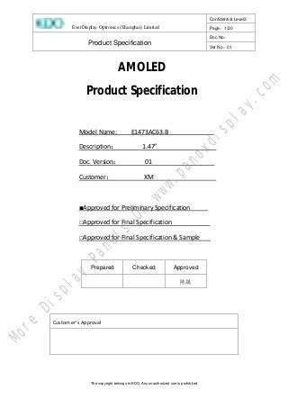
  • 1. EverDisplay Optronics (Shanghai) Limited Confidential Level3 Page:1/20 Product Specification Doc No: Ver No:01 The copyright belongs to EDO, Any unauthorized use is prohibited AMOLED Product Specification Model Name: E1473AC63.B Description: 1.47” Doc. Version: 01 Customer: XM ■Approved for Preliminary Specification □Approved for Final Specification □Approved for Final Specification & Sample Prepared Checked Approved 陈晟 Customer’s Approval M o r e D i s p l a y P a n e l s O n w w w . p a n o x d i s p l a y . c o m
  • 2. EverDisplay Optronics (Shanghai) Limited Confidential Level3 Page:2/20 Product Specification Doc No: Ver No:01 The copyright belongs to EDO, Any unauthorized use is prohibited Version History Version. No Date Contents Remark 01 2020.04.20 First Draft M o r e D i s p l a y P a n e l s O n w w w . p a n o x d i s p l a y . c o m
  • 3. EverDisplay Optronics (Shanghai) Limited Confidential Level3 Page:3/20 Product Specification Doc No: Ver No:01 The copyright belongs to EDO, Any unauthorized use is prohibited Contents 1 Scope.......................................................................................................................................................... 4 2 Features...................................................................................................................................................... 4 2.1 Product Applications ............................................................................................................................ 4 2.2 Product Features................................................................................................................................... 4 3 Mechanical Specifications ......................................................................................................................... 4 4 Maximum Rating ....................................................................................................................................... 4 5 Electrical Specifications............................................................................................................................. 5 5.1 Electrical Characteristics...................................................................................................................... 5 5.2 TP IC Recommended Operating Conditions ........................................................................................ 5 5.3 I/O Connection ................................................................................................................................... 10 5.4 Graphic memory writing direction ..................................................................................................... 11 5.5 Recommended Operating Sequence................................................................................................... 11 6 Electro-Optical Specification................................................................................................................... 14 7 Reliability................................................................................................................................................. 14 7.1 Environmental Test............................................................................................................................. 17 7.2 Electrical Test ..................................................................................................................................... 17 7.3 Mechanical Test.................................................................................................................................. 18 8 Outline Dimension Drawing.................................................................................................................... 19 9 Packing Specification................................................................................................................................ 20 10 The Control of Hazardous Substances...................................................................................................... 20 M o r e D i s p l a y P a n e l s O n w w w . p a n o x d i s p l a y . c o m
  • 4. EverDisplay Optronics (Shanghai) Limited Confidential Level3 Page:4/20 Product Specification Doc No: Ver No:01 The copyright belongs to EDO, Any unauthorized use is prohibited 1 Scope This Specification defines AMOLED manufactured by EverDisplay Optronics(Shanghai) Limited, from here on refer as EDO. In the case of any unspecified item, it may require both EDO and the party designs this module into its product to work out a solution. 2 Features 2.1 Product Applications Display/Touch terminals for Smart Watch 2.2 Product Features 1) Display color:16.7M (RGB x 24bits) 2) Display format:1.47”(194 RGB*368) 3) Pixel arrangement:Real RGB arrangement 4) Interface:Quad SPI 5) Driver IC: SH8501B (COF) 6) On cell touch sensor 7) Pixel format:only support 16bit GBRG 3553 3 Mechanical Specifications Item Specification unit LTPS Glass outline 19.36(V) x 36.17(W) mm Encapsulation Glass outline 19.36(V) x 35.42(W) mm Number of dots 194(W) x RGB x 368(H) dots Active area 17.46*33.12 mm Diagonal size 1.47 inch Pixel pitch 90*90 μm Glass thickness (LTPS/Encap. Glass/POL) 0.2/0.3/0.147 mm Weight TBD g 4 Maximum Rating Parameter Symbol Spec Unit Note Min. Typ. Max. Analog/boost power voltage VCI 3.2 3.3 3.4 V - I/O voltage VDDIO 1.7 1.8 1.9 V - M o r e D i s p l a y P a n e l s O n w w w . p a n o x d i s p l a y . c o m
  • 5. EverDisplay Optronics (Shanghai) Limited Confidential Level3 Page:5/20 Product Specification Doc No: Ver No:01 The copyright belongs to EDO, Any unauthorized use is prohibited Operating temperature Top -20 - 70 ℃ - Storage temperature Tstg -30 - 80 ℃ - 5 Electrical Specifications 5.1 Electrical Characteristics 5.1.1 Power Characteristic: Item Symbol Min. Typ. Max. Unit Remark AMOLED Power positive ELVDD 3.2 3.3 3.4 V - AMOLED power Negative ELVSS -3.4 -3.3 -3.2 V Ref Digital Power supply VDDIO 1.7 1.8 1.9 V Ref Analog Power supply VCI 3.2 3.3 3.4 V Ref 1) Normal Mode Power Supply: VDDIO =1.8V VCI=3.3V ELVDD=3.3V,ELVSS=-3.3V Frame Frequency: Fframe =60HZ @ 25degC, Brightness 450 nits, Display Condition Symbol Min. Typ. Max. Unit Remark 100% Pixel On,450nits Normal mode - 110 130 mW Ref 2) Idle Mode Power Supply: VDDIO=1.8V VCI=3.3 Frame Frequency: Fframe =15HZ @ 25degC, Brightness 50 nits, Display Condition Symbol Min. Typ. Max. Unit Remark 10% Pixel On,50nits Idle mode - 6.5 8.2 mW Ref 3) Deep Standby Mode Display Condition Symbol Min. Typ. Max. Unit Remark All Pixel Off,0nits/ Vci off/Vddio on Standby mode - - 50 μW - 5.2 Driver IC SH8501B (refer to the datasheet) 5.3 TP IC ZTW622 M o r e D i s p l a y P a n e l s O n w w w . p a n o x d i s p l a y . c o m
  • 6. EverDisplay Optronics (Shanghai) Limited Confidential Level3 Page:6/20 Product Specification Doc No: Ver No:01 The copyright belongs to EDO, Any unauthorized use is prohibited 5.3.1 Basic Specifications No. Item Specification Description Remark 1 Project ID 10 Bytes 1.The ninth byte increased by 1 if sensor or circuit changed and cannot use one TP FW compatible for them. 2.No need to read it by FW 2 Communication Protocol to Host I2C 3 I2C Address TBD 4 Touch Origination Dot Left-up Refer AMOLED 5 Finger 2 6 Respond Time(60HZ~120HZ) Active:18 ms(Avg)/ 30ms(Max) Active mode Response Time(60HZ~120HZ) TBD Doze mode 7 Point Sensitivity ≤Ф5mm Report Percentage=10 0% (Both center area and edge area) Arm of robot with 5mm diameter copper 8 Accuracy(Ф7mm) Edge area<2.0mm Center area<1.5mm 9 Precision(Ф7mm) Edge area <0.5mm Center area <0.4mm 10 Jitter (Ф7mm) Edge area <0.5mm Center area <0.4mm 11 Move Sensitivity ≤Ф 5mm 12 Linearity (Ф7mm) Edge area <2.0mm Center area <1.5mm 13 Adjacent Finger Finger Distance <15mm Center to Center M o r e D i s p l a y P a n e l s O n w w w . p a n o x d i s p l a y . c o m
  • 7. EverDisplay Optronics (Shanghai) Limited Confidential Level3 Page:7/20 Product Specification Doc No: Ver No:01 The copyright belongs to EDO, Any unauthorized use is prohibited 14 Palm & Face Ø14mm 15 Water Proof Refer to Note 1 1.No ghost finger, 2.No fault ID 3.No sensitivity reduce when water wiped off Note 1 16 Move with low speed (2mm/s)- Handwork NO fault ID, especial missing point near edge area 17 Fast drawing(1 fingers)- Handwork NO fault ID report to host interface Touch Panel must detect touch ID fast and exactly 18 Fast Tap ( 2 fingers)-Handwork NO fault ID report to host interface 19 Common-mode interference ≥2.5Vpp 1.Input wave: Sine Wave Frequency: <500KHz 2. support standard Charger 20 Ripple interference 100mv Based on Power typ. Value mentioned in item7.2 5.3.2 Waterproof touch Requirement No Item Water proof Remark 1 Water Spray Test 1.No ghost finger, 2.No fault ID 3.No sensitivity reduce when water wiped off 2 Drop Test 1.No ghost finger reported to host 2.Wipe off water the water area 3.No sensitivity reduce when water wiped off 3 Bathroom Test 1.No ghost finger, 2.No fault ID 3.No sensitivity reduce when water wiped off M o r e D i s p l a y P a n e l s O n w w w . p a n o x d i s p l a y . c o m
  • 8. EverDisplay Optronics (Shanghai) Limited Confidential Level3 Page:8/20 Product Specification Doc No: Ver No:01 The copyright belongs to EDO, Any unauthorized use is prohibited 3 Wash with running water 1.No ghost finger reported to host 2.Wipe off water the water area 4 Operate with Wet finger 1.No ghost finger, 2.No fault ID 3.No sensitivity reduce when water wiped off 5 Operate with Sweat 1.No ghost finger, 2.No fault ID 3.No sensitivity reduce when water wiped off 5.3.3 Touch IC Specifications NO. Item Specification Description Remark 1 Communication Host I2C to Host Speed: ≥400KHZ 2 SPI Communication to Host NO 3 Main Oscillator Frequency Shift ≤ 3% 1, (Max – Min)/Max 2, between -20℃~60℃ 4 Auxiliary Oscillator Frequency Shift ≤ 15 % 1, (Max – Min)/Max 2, between -20℃~60℃ 5 Power on latency ≤ 100 ms from power up to the 1st Frame 6 Maximum Sensing Frequency ≥ 500 KHz Tx Sensing Frequency 7 Minimum Sensing Frequency ≤ 50 KHz Tx Sensing Frequency 8 Sensing Frequency resolution ≤ 5 KHz 9 Software Update Must support 1, If FW update fails for some reason, IC must have secured bootloader section which can inform host the project code etc. and start re-flash operation per host command 2, Can not affect the other information 11 Calibration time If the IC need do Calibration 1,must calibrate and save in factory 2, driver can calibrate the IC automatically no manual calibration M o r e D i s p l a y P a n e l s O n w w w . p a n o x d i s p l a y . c o m
  • 9. EverDisplay Optronics (Shanghai) Limited Confidential Level3 Page:9/20 Product Specification Doc No: Ver No:01 The copyright belongs to EDO, Any unauthorized use is prohibited 12 <200 ms Calibration must be done in 200ms 13 Timing request Mode Switching Latency from idle mode to active mode less than 16 ms Reference : Note 1 :TP Water Proof The presence of moisture on the surface of touch can affect touch performance. Performance will vary based on the amount of moisture and its properties. In the test we will define the particular requirement in the document. Test procedure: Drop: Size : ø10 mm diameter drop,4 drops Spray size: 3ml once Water Drop Water Spray Test Procedure: Test 1-Drop Test: Step 1: Make 4 drops water on the surface of touch, each drop with 10mm diameter. Step 2: Test the area (without water area) handwork, and test it again after wiped off water Step 3: Observe whether the water area report ghost finger Test 2-Spray test: Step 1: Spray the water on the surface of touch for 3ml. Step 2: Keep the water on the surface of touch for 60 seconds. Step 3: Wipe off the water then test the function 10mm M o r e D i s p l a y P a n e l s O n w w w . p a n o x d i s p l a y . c o m
  • 10. EverDisplay Optronics (Shanghai) Limited Confidential Level3 Page:10/20 Product Specification Doc No: Ver No:01 The copyright belongs to EDO, Any unauthorized use is prohibited 5.4 I/O Connection 5.4.1 Main FPC Bonding PAD Define Pin No. Symbol I/O Function Description 1 TP_OPT_VDDIO I/O 1.8V power for TP&OPTIC 2 GND Power Ground 3 OPTIC_INT I/O ALS INT 4 TP_OPT_I2C_SDA I/O TP & OPT I2C DATA 5 TP_OPT_I2C_SCL I/O TP & OPT I2C CLK 6 TP_VDD Power 2.8V power for TP 7 GND Power Ground 8 AM_SPI_CSX I OLED QSPI interface 9 AM_SPI_SCL I OLED QSPI interface 10 REST I OLED Device reset signal(0:enable;1:Disable) 11 GND Power Ground 12 TE O Synchronous signal output from panel to avoid tearing effect 13 VDDIO Power OLED Power supply for interface system 14 GND Power Ground 15 ELVDD Power OLED Power Supply 16 ELVDD Power OLED Power Supply 17 GND Power Ground 18 GND Power Ground 19 ELVSS Power OLED Power Supply 20 ELVSS Power OLED Power Supply 21 SWDIO(NC) - Floating 22 VCI Power AMOLED power 23 GND Power Ground 24 Swire I Swire control interface. 25 AM_SPI_SD0 I/O OLED QSPI interface 26 AM_SPI_SD1 I/O OLED QSPI interface 27 AM_SPI_SD2 I/O OLED QSPI interface 28 AM_SPI_SD3 I/O OLED QSPI interface 29 NC(MTP) -- Floating 30 TP_RST I/O TP Reset 31 TP_INT I/O TP INT 32 GND Power Ground 33 NFC_P I/O NFC TX1 34 NFC_N I/O NFC TX2 M o r e D i s p l a y P a n e l s O n w w w . p a n o x d i s p l a y . c o m
  • 11. EverDisplay Optronics (Shanghai) Limited Confidential Level3 Page:11/20 Product Specification Doc No: Ver No:01 The copyright belongs to EDO, Any unauthorized use is prohibited 5.5 Graphic memory writing direction 5.6 Recommended Operating Sequence 5.6.1 Power on sequence 5.6.2 Power off sequence 5.6.3 Quad SPI Interface Characteristics M o r e D i s p l a y P a n e l s O n w w w . p a n o x d i s p l a y . c o m
  • 12. EverDisplay Optronics (Shanghai) Limited Confidential Level3 Page:12/20 Product Specification Doc No: Ver No:01 The copyright belongs to EDO, Any unauthorized use is prohibited 5.6.4 Display Reset Timing M o r e D i s p l a y P a n e l s O n w w w . p a n o x d i s p l a y . c o m
  • 13. EverDisplay Optronics (Shanghai) Limited Confidential Level3 Page:13/20 Product Specification Doc No: Ver No:01 The copyright belongs to EDO, Any unauthorized use is prohibited 5.6.5 TP Reset Timing M o r e D i s p l a y P a n e l s O n w w w . p a n o x d i s p l a y . c o m
  • 14. EverDisplay Optronics (Shanghai) Limited Confidential Level3 Page:14/20 Product Specification Doc No: Ver No:01 The copyright belongs to EDO, Any unauthorized use is prohibited 6 Electro-Optical Specification Test condition:IOVCC=1.8V , VCI=3.3V ,Ta=25℃ Item Symbol Condition Value Unit Note Min Typ Max Luminance θ=0° 400 450 500 cd/m2 Note 1 Uniformity 85 - % Note 2 Viewing Angle Left θL Cr≥200 80 85 - Deg. Note 3 Right θR 80 85 - Top ψT 80 85 - Bottom ψB 80 85 - Contrast Ratio CR θ=0° 50000 100000 - - Note 4 Response Time Tr+Tf - 2 3 ms Note 5 Color Coordinate of CIE1931 Red X θ=0° 0.656 0.686 0.716 - - Y 0.283 0.313 0.343 Green X 0.195 0.235 0.275 Y 0.685 0.725 0.765 Blue X 0.113 0.143 0.173 Y 0.014 0.044 0.074 White X 0.28 0.30 0.32 Y 0.29 0.31 0.33 NTSC Ratio NTSC CIE1931 100 - % - Flicker - - - - -30 dB - Gamma - - 1.9 2.2 2.5 Note 6 Crosstalk △CT - - - 1.1 Note 7 Color shift θL=30° 6 JNCD OLED Life Time 0.95*(TYP brightness) At 25℃,with white color pattern 200 hrs Note8 Note 1: Luminance measurement The test condition is measured on the surface of AMOLED module at 25℃. • Measurement equipment CS2000 or similar equipment (Field of view:1deg,Distance:50cm) • Measuring surroundings: Dark room. • Measuring temperature: Ta=25℃. • Adjust operating voltage to get optimum contrast at the center of the display. M o r e D i s p l a y P a n e l s O n w w w . p a n o x d i s p l a y . c o m
  • 15. EverDisplay Optronics (Shanghai) Limited Confidential Level3 Page:15/20 Product Specification Doc No: Ver No:01 The copyright belongs to EDO, Any unauthorized use is prohibited Note 2: Uniformity The luminance uniformity is calculated by using following formula: △Bp = Bp (Min.) / Bp (Max.)×100 (%) Bp (Max.) = Maximum brightness in 5 measured spots Bp (Min.) = Minimum brightness in 5 measured spots. Note 3: The definition of Viewing Angle Refer to the graph below marked by θ and Ф Note 4: The definition of Contrast Ratio: Luminance When AMOLED is at “White” state Contrast Ratio (CR) = Luminance When AMOLED is at “Black” state Note 5: Definition of Response time. M o r e D i s p l a y P a n e l s O n w w w . p a n o x d i s p l a y . c o m
  • 16. EverDisplay Optronics (Shanghai) Limited Confidential Level3 Page:16/20 Product Specification Doc No: Ver No:01 The copyright belongs to EDO, Any unauthorized use is prohibited The output signals of photo detector are measured when the input signals are changed from “black” to “white” (Voltage falling time) and from “white” to “black” (Voltage rising time), respectively. The response time is defined as the time interval between the 10% and 90% of amplitudes. Refer to figure as below. Note 6: Gamma curve The whole curve’s tolerance must control within +/-0.3, test the gray scale below: 8, 16, 25, 33, 41, 49, 58, 66, 74, 82, 90, 99, 107, 115, 123, 132, 140, 148, 156, 165, 173, 181, 189, 197,206, 214, 222, 230, 239, 255 Note 7: Crosstalk There should be no visible cross-talk in normal direction of the display when the two “Cross-talk Test Patterns” below are loaded. △Bp (Max.) = Maximum value in △Bp1~△Bp4. △Bp (Min.) = Minimum value in △Bp1~△Bp4. △CT=△Bp (Max.)/ △Bp(Min.). △CT must be less than 1.10 Cross-talk Test Pattern Note 7: Life Time OLED life time is defined by the Minimum Duration Time that the luminance is decayed to a specific ratio (ex. 92%) of initial state. Test Pattern under duration period: L255 White M o r e D i s p l a y P a n e l s O n w w w . p a n o x d i s p l a y . c o m
  • 17. EverDisplay Optronics (Shanghai) Limited Confidential Level3 Page:17/20 Product Specification Doc No: Ver No:01 The copyright belongs to EDO, Any unauthorized use is prohibited 7 Reliability 7.1 Environmental Test Item Main spec No. of failures / No. of examinations High Temperature Operation 70℃/ 240hrs 0/5 Low Temperature Operation -20℃/ 240hrs 0/5 High Temperature Storage 80℃/ 240hrs 0/5 Low Temperature Storage -30℃/ 240hrs 0/5 High Temperature Humidity Operation 60℃/90%RH/ 240hrs 0/16 Thermal Shock -40℃~80℃ dwell time=0.5hr, 100cycles. 0/16 TP Sensor-Film 表面能测试 达因笔画线 5 秒后成 A 状 0/10 TP FPC 拉拔力测试 >5N/CM 0/5 TP FPC 抗弯折测试 20 次,同位置反向弯折 20 次 0/5 撕膜 ESD 测试 静电峰值电压<500V 0/10 7.2 Electrical Test Item Main spec Note Air Discharge ±4 kV , 150pF/330Ω (Module level; without CG) 5Points, Each 10times. After one time discharge, panel and gun touch the ground, through the whole test, turn on ion fan. No degradation of OLED performance after this test. Contact Discharge ±2kV, 150pF/330Ω (Module level; without CG) M o r e D i s p l a y P a n e l s O n w w w . p a n o x d i s p l a y . c o m
  • 18. EverDisplay Optronics (Shanghai) Limited Confidential Level3 Page:18/20 Product Specification Doc No: Ver No:01 The copyright belongs to EDO, Any unauthorized use is prohibited 7.3 Mechanical Test Test item Test condition Note Packing vibration-proof test 2g, f=10->55->10Hz apply in each of X, Y, and Z direction for 30 min Package Packing Drop test Drop the packing from 60cm height, 6-faces, 3-edges and 1-corner(one time for each) Package M o r e D i s p l a y P a n e l s O n w w w . p a n o x d i s p l a y . c o m
  • 19. EverDisplay Optronics (Shanghai) Limited Confidential Level3 Page:19/20 Product Specification Doc No: Ver No:01 The copyright belongs to EDO, Any unauthorized use is prohibited 8 Outline Dimension Drawing M o r e D i s p l a y P a n e l s O n w w w . p a n o x d i s p l a y . c o m
  • 20. EverDisplay Optronics (Shanghai) Limited Confidential Level3 Page:20/20 Product Specification Doc No: Ver No:01 The copyright belongs to EDO, Any unauthorized use is prohibited 9 Packing Specification TBD 10 The Control of Hazardous Substances The control of Hazardous substances refer to EDO document 《有害物质管控标准书》 (Standard document for the Control of Hazardous substances) EDO –IS- 110, the latest version. M o r e D i s p l a y P a n e l s O n w w w . p a n o x d i s p l a y . c o m