E1392AM1 1.39 inch OLED 400X400/EDO
•
0 likes•4 views

Model: H139BLN01.0 (AUO 24 pins Left side interface) E1392AM1 (EDO 20 pins Right Side Interface) Display Brand AUO/EDO Interface MIPI Screen Size 1.39 Orientation Landscape Display Color Full Color Manufacturer AUO/EDO Resolution 400(RGB)×400 Driver IC RM69080/RM67160 Active Area (mm) 35.4 × 35.4 (H×V) Luminance 350 or 300 cd/m² (Typ.) Viewing Angle 80/80/80/80 (Min.)(CR≥1600) Color Depth 16.7M 100% (CIE1931) Mass 2.15±0.33g Refresh Rate 30 Hz Signal Type MIPI (1 data lane) , Connector , 24 pins/20 pins OLED Product Page https://www.panoxdisplay.com/amoled/1-39-round-amoled-full-color-400x400.html

Recommended
More Related Content
More from Panox Display
More from Panox Display (8)
E1392AM1 1.39 inch OLED 400X400/EDO
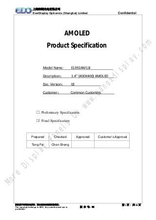
- 1. 上海和辉光电有限公司 EverDisplay Optronics (Shanghai) Limited Confidential 版权属于和辉光电所有,禁止任何未经授权的使用。 The copyright belongs to EDO, Any unauthorized use is prohibited. 版 本 号:02 第 1 页 / 共 19 页 √ AMOLED Product Specification Model Name: E1392AM1.B Description: 1.4” (400X400) AMOLED Doc. Version: 02 Customer: Common Customers □ Preliminary Specification □ Final Specification Prepared Checked Approved Customer’s Approval Teng Fei Chen Sheng M o r e D i s p l a y P a n e l s O n w w w . p a n o x d i s p l a y . c o m
- 2. 上海和辉光电有限公司 EverDisplay Optronics (Shanghai) Limited Confidential 版权属于和辉光电所有,禁止任何未经授权的使用。 The copyright belongs to EDO, Any unauthorized use is prohibited. 版 本 号:02 第 2 页 / 共 19 页 Reversion History Reversion. No Date Contents Remark 01 2015-1-13 First Draft 02 2015-5-15 Rev. B 03 2016-10-17 Updated 2D Drawings M o r e D i s p l a y P a n e l s O n w w w . p a n o x d i s p l a y . c o m
- 3. 上海和辉光电有限公司 EverDisplay Optronics (Shanghai) Limited Confidential 版权属于和辉光电所有,禁止任何未经授权的使用。 The copyright belongs to EDO, Any unauthorized use is prohibited. 版 本 号:02 第 3 页 / 共 19 页 Contents Contents .......................................................................................................................................................... 3 1 Scope.......................................................................................................................................................... 4 2 Features ..................................................................................................................................................... 4 2.1 Product Applications............................................................................................................................. 4 2.2 Product Features .................................................................................................................................. 4 3 Mechanical Specifications.......................................................................................................................... 4 4 Maximum Rating........................................................................................................................................ 4 5 Electrical Specifications.............................................................................................................................. 5 5.1 Electrical Characteristics....................................................................................................................... 5 5.2 I/O Connection and Block Diagrams..................................................................................................... 8 5.3 Recommended Operating Sequence.................................................................................................. 10 5.4 AC Characteristics(MIPI)................................................................................................................ 10 6 Electro-Optical Specification.................................................................................................................... 13 7 Reliability.................................................................................................................................................. 16 7.1 Environmental Test............................................................................................................................. 16 7.2 Electrical Test...................................................................................................................................... 16 7.3 Mechanical Test.................................................................................................................................. 17 8 Handling Precautions............................................................................................................................... 17 9 Outline Dimension Drawing..................................................................................................................... 18 10 Packing Specification................................................................................................................................ 19 M o r e D i s p l a y P a n e l s O n w w w . p a n o x d i s p l a y . c o m
- 4. 上海和辉光电有限公司 EverDisplay Optronics (Shanghai) Limited Confidential 版权属于和辉光电所有,禁止任何未经授权的使用。 The copyright belongs to EDO, Any unauthorized use is prohibited. 版 本 号:02 第 4 页 / 共 19 页 1 Scope This Specification defines AMOLED manufactured by EverDisplay Optronics(Shanghai) Limited, from here on refer as EDO. In the case of any unspecified item, it may require both EDO and the party designs this module into its product to work out a solution. 2 Features 2.1 Product Applications Smart Watch 2.2 Product Features 1) Display color:16.7M (RGB x 8bits) 2) Display format:1.4”(400RGBx400) 3) Pixel arrangement:Real RGB arrangement 4) Interface:MIPI 1-lane 3 Mechanical Specifications Item Specification unit Dimension outline 38.6 x 40.5 x 0.67 mm LTPS Glass outline 38.6 x 40.5 mm Encapsulation Glass outline φ38.6 mm Number of dots 400(W) x RGB x 400(H) dots Active area φ35.4 mm Diagonal size 1.39 inch Pixel pitch 29.5 x 88.5 μm Glass thickness (LTPS/encapsulation glass) 0.2 / 0.2 mm Weight 2 g Note: Refer to 9 Outline Dimension Drawing 4 Maximum Rating Parameter Symbol Spec Unit Note Min. Typ. Max. Analog/boost power voltage VCI -0.3 - - V - I/O voltage VDDIO -0.3 - - V - Operating temperature Top -20 - 60 ℃ - Storage temperature Tstg -30 - 70 ℃ - M o r e D i s p l a y P a n e l s O n w w w . p a n o x d i s p l a y . c o m
- 5. 上海和辉光电有限公司 EverDisplay Optronics (Shanghai) Limited Confidential 版权属于和辉光电所有,禁止任何未经授权的使用。 The copyright belongs to EDO, Any unauthorized use is prohibited. 版 本 号:02 第 5 页 / 共 19 页 5 Electrical Specifications 5.1 Electrical Characteristics 5.1.1 Power Characteristic: Item Symbol Min. Typ. Max. Unit Remark AMOLED Power positive ELVDD 4.55 4.6 4.65 V - AMOLED power Negative ELVSS -2.45 -2.4 -2.35 V Ref Digital Power supply VDDIO 1.65 1.8 1.95 V Ref Analog Power supply VCI 2.7 2.8 2.9 V Ref 1) Normal Mode Power Supply: IOVCC=1.8V VCI=2.8V Frame Frequency: Fframe =60HZ @ 25degC, Brightness 300 nits, Command Mode, Display Condition Symbol Min. Typ. Max. Unit Remark 100% Pixel On 300nits IELVDD /ELVSS - 21.0 25.4 mA Ref IVCI - 6.0 7.2 mA Ref IVDDIO - 2.0 2.4 mA Ref 50% Pixel On 150nits IELVDD /ELVSS - 5.2 6.2 mA Ref IVCI - 6.6 8.0 mA Ref IVDDIO - 2.0 2.4 mA Ref 10% Pixel On 50nits IELVDD /ELVSS - 0.4 0.5 mA Ref IVCI - 7.2 8.6 mA Ref IVDDIO - 2.0 2.4 mA Ref 2) Idle Mode Power Supply: IOVCC=1.8V VCI=2.8V Frame Frequency: Fframe =15HZ @ 25degC, Brightness 30 nits, Display Condition Symbol Min. Typ. Max. Unit Remark 10% Pixel On 30 nits IELVDD /ELVSS - - - mA Supplied by Driver IC IVCI - 3.0 3.6 mA Ref IVDDIO - 1.0 1.2 mA Ref 3) Deep Standby Mode Display Condition Symbol Min. Typ. Max. Unit Remark Deep Standby IVCI - - 1 uA - IVDDIO - - 0 uA - M o r e D i s p l a y P a n e l s O n w w w . p a n o x d i s p l a y . c o m
- 6. 上海和辉光电有限公司 EverDisplay Optronics (Shanghai) Limited Confidential 版权属于和辉光电所有,禁止任何未经授权的使用。 The copyright belongs to EDO, Any unauthorized use is prohibited. 版 本 号:02 第 6 页 / 共 19 页 5.1.2 Power supply circuit application (This is for reference only): 1) RT4723 2) SM3321 3) TPS65631W M o r e D i s p l a y P a n e l s O n w w w . p a n o x d i s p l a y . c o m
- 7. 上海和辉光电有限公司 EverDisplay Optronics (Shanghai) Limited Confidential 版权属于和辉光电所有,禁止任何未经授权的使用。 The copyright belongs to EDO, Any unauthorized use is prohibited. 版 本 号:02 第 7 页 / 共 19 页 4) STAM1332 M o r e D i s p l a y P a n e l s O n w w w . p a n o x d i s p l a y . c o m
- 8. 上海和辉光电有限公司 EverDisplay Optronics (Shanghai) Limited Confidential 版权属于和辉光电所有,禁止任何未经授权的使用。 The copyright belongs to EDO, Any unauthorized use is prohibited. 版 本 号:02 第 8 页 / 共 19 页 5.2 I/O Connection and Block Diagrams 5.2.1 I/O Connection # Pin_name I/O Description 1 ELVSS1 Power AMOLED power Negative 2 ELVDD1 Power AMOLED power Positive 3 ELVSS2 Power AMOLED power Negative 4 ELVDD2 Power AMOLED power Positive 5 ELVSS3 Power AMOLED power Negative 6 ELVDD3 Power AMOLED power Positive 7 VCI Power Driver IC analog supply 8 GND2 Power The power ground 9 VDDIO Power Driver IC digital I/O supply 10 DSI_D0N I/O MIPI DSI data0- 11 GND1 Power The power ground 12 DSI_D0P I/O MIPI DSI data0+ 13 TE O Tear effect output 14 GND3 Power The power ground 15 VPP Power Power supply for OTP. Leave the pin to open when not in use. 16 DSI_CLKN I/O MIPI DSI clock- 17 REST I This signal will reset the device and must be applied to properly initialize the chip. Active low. 18 DSI_CLKP I/O MIPI DSI clock+ 19 SWIRE O Swire protocol setting pin of Power IC 20 GND4 Power The power ground M o r e D i s p l a y P a n e l s O n w w w . p a n o x d i s p l a y . c o m
- 9. 上海和辉光电有限公司 EverDisplay Optronics (Shanghai) Limited Confidential 版权属于和辉光电所有,禁止任何未经授权的使用。 The copyright belongs to EDO, Any unauthorized use is prohibited. 版 本 号:02 第 9 页 / 共 19 页 AMOLED PANEL FPC COF Driver IC LTPS GOA LTPS GOA Data Driver OP output Timing Controller DC/DC Passive Components for Driver IC Connector Host Interface M o r e D i s p l a y P a n e l s O n w w w . p a n o x d i s p l a y . c o m
- 10. 上海和辉光电有限公司 EverDisplay Optronics (Shanghai) Limited Confidential 版权属于和辉光电所有,禁止任何未经授权的使用。 The copyright belongs to EDO, Any unauthorized use is prohibited. 版 本 号:02 第 10 页 / 共 19 页 5.3 Recommended Operating Sequence 5.3.1 Power on sequence 5.3.2 Power off sequence 5.4 AC Characteristics(MIPI) 5.4.1 HS Data Transmission Burst 5.4.2 HS Clock Transmission M o r e D i s p l a y P a n e l s O n w w w . p a n o x d i s p l a y . c o m
- 11. 上海和辉光电有限公司 EverDisplay Optronics (Shanghai) Limited Confidential 版权属于和辉光电所有,禁止任何未经授权的使用。 The copyright belongs to EDO, Any unauthorized use is prohibited. 版 本 号:02 第 11 页 / 共 19 页 5.4.3 Turnaround Procedure 5.4.4 Timing Parameters Symbol Description Min Typ Max Unit TREOT 30%-85% rise time and fall time - - 35 ns TCLK-MISS Timeout for receiver to detect absence of Clock transitions and disable the Clock Lane HS-RX. - - 60 ns TCLK-POST*1 Time that the transmitter continues to send HS clock after the last associated Data Lane has transitioned to LP Mode. Interval is defined as the period from the end of THS-TRAIL to the beginning of TCLK-TRAIL. 60ns + 52*UI (For DCS) - - ns TCLK-PRE Time that the HS clock shall be driven by the transmitter prior to any associated Data Lane beginning the transition from LP to HS mode. 8 - - ns TCLK-SETTLE Time interval during which the HS receiver shall ignore any Clock Lane HS transitions, starting from the beginning of TCLK-PRE. 95 - 300 ns TCLK-TERM-EN Time for the Clock Lane receiver to enable the HS line termination,starting from the time point when Dn crosses VIL,MAX. Time for Dn to reach VTERM-EN 38 ns THS-SETTLE Time interval during which the HS receiver shall ignore any Data Lane HS transitions, starting from 85 ns + 6*UI 145 ns + 10*UI ns M o r e D i s p l a y P a n e l s O n w w w . p a n o x d i s p l a y . c o m
- 12. 上海和辉光电有限公司 EverDisplay Optronics (Shanghai) Limited Confidential 版权属于和辉光电所有,禁止任何未经授权的使用。 The copyright belongs to EDO, Any unauthorized use is prohibited. 版 本 号:02 第 12 页 / 共 19 页 the beginning of THSPREPARE. TEOT Time from start of THS-TRAIL or TCLK-TRAIL period to start of LP-11 state - - 105ns+48*UI ns THS-EXIT(1) time to drive LP-11 after HS burst 100 - - ns THS-PREPARE Time to drive LP-00 to prepare for HS transmission 40ns + 4*UI - 85ns+6*UI ns THS-PREPARE + THS-ZERO THS-PREPARE + Time to drive HS-0 before the Sync sequence 145ns + 10*UI - - ns THS-SKIP Time-out at RX to ignore transition period of EoT 40 - 55ns+4*UI ns THS-TRAIL Time to drive flipped differential state after last payload data bit of a HS transmission burst 60 + 4*UI - - ns TLPX Length of any Low-Power state period 50 - - ns Ratio TLPX Ratio of TLPX(MASTER)/TLPS(SLAVE) between Master and Slave side 2/3 - 3/2 ns TTA-GET Time to drive LP-00 by new TX 5*TLPX 5*TLPX 5*TLPX ns TTA-GO Time to drive LP-00 after Turnaround Request 4*TLPX 4*TLPX 4*TLPX ns TTA-SURE Time-out before new TX side starts driving TLPX - 2*TLPX ns 5.4.5 Timing requirements for RESETB When RESETB of the reset pin equals to Low, it will be in the condition of reset. When it is in the condition of reset, it will make the device recover the initial set. However, in order to avoid the reset noise cause reset, there is a mechanism to judge about whether the reset is needed or not. The closed interval of Low can be shown as the following. (Test condition: VDDIO=1.65V~3.6V, VSS=0V, TA=-20℃~+70℃) Parameter Symbol Conditions Spec Unit Min. Typ. Max. Reset low pulse width Trst - 20 - - µs Table: Reset timing M o r e D i s p l a y P a n e l s O n w w w . p a n o x d i s p l a y . c o m
- 13. 上海和辉光电有限公司 EverDisplay Optronics (Shanghai) Limited Confidential 版权属于和辉光电所有,禁止任何未经授权的使用。 The copyright belongs to EDO, Any unauthorized use is prohibited. 版 本 号:02 第 13 页 / 共 19 页 Trst 20% 20% RESETB Figure: Reset timing 6 Electro-Optical Specification Test condition:IOVCC=1.8V , VCI=2.8V ,Ta=25℃ Item Symbol Condition Value Unit Note Min Typ Max Luminance θ=0° =0° 250 300 - cd/m2 Note 1 Uniformity 80 - % Note 2 Viewing Angle Left θL Cr≥200 80 85 - Deg. Note 3 Right θR 80 85 - Top ψT 80 85 - Bottom ψB 80 85 - Contrast Ratio CR θ=0° =0° 5000 10000 - - Note 4 Response Time Tr+Tf - 2 4 ms Note 5 Color Coordinate of CIE1931 Red X θ=0° =0° 0.63 0.66 0.69 - - Y 0.31 0.34 0.37 Green X 0.16 0.21 0.26 Y 0.69 0.74 0.79 Blue X 0.09 0.13 0.17 Y 0.02 0.06 0.10 White X 0.27 0.30 0.33 Y 0.28 0.31 0.34 NTSC Ratio NTSC CIE1931 85 100 - % - Flicker - - - -30 - dB - Gamma - - 1.9 2.2 2.5 Note 6 Crosstalk △ CT - - - 1.1 Note 7 Note 1: Luminance measurement The test condition is measured on the surface of AMOLED module at 25℃. • Measurement equipment CS2000 or similar equipment (Field of view:1deg,Distance:50cm) • Measuring surroundings: Dark room. • Measuring temperature: Ta=25℃. • Adjust operating voltage to get optimum contrast at the center of the display. • Measuring Pattern: M o r e D i s p l a y P a n e l s O n w w w . p a n o x d i s p l a y . c o m
- 14. 上海和辉光电有限公司 EverDisplay Optronics (Shanghai) Limited Confidential 版权属于和辉光电所有,禁止任何未经授权的使用。 The copyright belongs to EDO, Any unauthorized use is prohibited. 版 本 号:02 第 14 页 / 共 19 页 Note 2: Uniformity The luminance uniformity is calculated by using following formula: △Bp = Bp (Min.) / Bp (Max.)×100 (%) Bp (Max.) = Maximum brightness in 5 measured spots Bp (Min.) = Minimum brightness in 5 measured spots. Note 3: The definition of Viewing Angle Refer to the graph below marked by θ and Ф M o r e D i s p l a y P a n e l s O n w w w . p a n o x d i s p l a y . c o m
- 15. 上海和辉光电有限公司 EverDisplay Optronics (Shanghai) Limited Confidential 版权属于和辉光电所有,禁止任何未经授权的使用。 The copyright belongs to EDO, Any unauthorized use is prohibited. 版 本 号:02 第 15 页 / 共 19 页 Note 4: The definition of Contrast Ratio: Luminance When AMOLED is at “White” state Contrast Ratio (CR) = Luminance When AMOLED is at “Black” state Note 5: Definition of Response time. The output signals of photo detector are measured when the input signals are changed from “black” to “white” (Voltage falling time) and from “white” to “black” (Voltage rising time), respectively. The response time is defined as the time interval between the 10% and 90% of amplitudes. Refer to figure as below. Note 6: Gamma curve The whole curve’s tolerance must control within +/-0.3, test the gray scale below: 8, 16, 25, 33, 41, 49, 58, 66, 74, 82, 90, 99, 107, 115, 123, 132, 140, 148, 156, 165, 173, 181, 189, 197,206, 214, 222, 230, 239, 247 Note 7: Crosstalk There should be no visible cross-talk in normal direction of the display when the two “Cross-talk Test Patterns” below are loaded. △Bp (Max.) = Maximum value in △Bp1~△Bp4. △Bp (Min.) = Minimum value in △Bp1~△Bp4. △CT=△Bp (Max.)/ △Bp(Min.). △CT must be less than 1.10 M o r e D i s p l a y P a n e l s O n w w w . p a n o x d i s p l a y . c o m
- 16. 上海和辉光电有限公司 EverDisplay Optronics (Shanghai) Limited Confidential 版权属于和辉光电所有,禁止任何未经授权的使用。 The copyright belongs to EDO, Any unauthorized use is prohibited. 版 本 号:02 第 16 页 / 共 19 页 Cross-talk Test Pattern 7 Reliability 7.1 Environmental Test Item Main spec No. of failures / No. of examinations Note High Temperature Operation 70℃/ 128hours 0/5 Low Temperature Operation -20℃/ 128hours 0/5 High Temperature Storage 80℃/ 128hours 0/5 Low Temperature Storage -30℃/ 128hours 0/5 High Temperature Humidity Operation 60℃/90%RH 128hours 0/5 Thermal Shock -40℃~80℃ 0.5hr, 30 cycles 0/5 7.2 Electrical Test Item Main spec Note Air Discharge ±4kV , 150pF/330Ω (Module level) 5Points, Each 2times. No degradation of OLED performance after this test. Contact Discharge ±4kV, 150pF/330Ω (Module level) M o r e D i s p l a y P a n e l s O n w w w . p a n o x d i s p l a y . c o m
- 17. 上海和辉光电有限公司 EverDisplay Optronics (Shanghai) Limited Confidential 版权属于和辉光电所有,禁止任何未经授权的使用。 The copyright belongs to EDO, Any unauthorized use is prohibited. 版 本 号:02 第 17 页 / 共 19 页 7.3 Mechanical Test Item Main spec Note Drop Test Drop the packing from 75cm height, 3 times for 6-faces, 3-edges and 1-corner Package Vibration-proof test 2g, f=10->55->10Hz apply in each of X, Y, and Z direction for 30 min Package 8 Handling Precautions 8.1 When cleaning ITO pad, avoid using hard and abrasive material or corrosive solution 8.2 Keep module away from direct sunlight or fluorescent light, and keep it at room temperature and humidity 8.3 Strong impact & pressure on module and packing is prohibited 8.4 Following normal power on/off sequence is necessary for preventing abnormal display or permanent damage to display 8.5 Optimal contrast ratio under ideal voltage is AMOLED module’s characteristic, hence it is recommended a voltage control function available 8.6 Image sticking may occur if an image displays for an extended period of time 8.7 When interfered by system’s overall mechanical design, an abnormal display may occur 8.8 After considering emitting energy, you should plan your design to satisfy EMI standards. 8.9 Host side should place a surge-prevent circuit at power trace (ie: VCI, Vddi) to protect AMOLED module. M o r e D i s p l a y P a n e l s O n w w w . p a n o x d i s p l a y . c o m
- 18. 上海和辉光电有限公司 EverDisplay Optronics (Shanghai) Limited Confidential 版权属于和辉光电所有,禁止任何未经授权的使用。 The copyright belongs to EDO, Any unauthorized use is prohibited. 版 本 号:02 第 18 页 / 共 19 页 9 Outline Dimension Drawing M o r e D i s p l a y P a n e l s O n w w w . p a n o x d i s p
- 19. 上海和辉光电有限公司 EverDisplay Optronics (Shanghai) Limited Confidential 版权属于和辉光电所有,禁止任何未经授权的使用。 The copyright belongs to EDO, Any unauthorized use is prohibited. 版 本 号:02 第 19 页 / 共 19 页 10Packing Specification E1392AM1_D_包装建 议书_V1.0_ME_150720.doc M o r e D i s p l a y P a n e l s O n w w w . p a n o x d i s p l a y . c o m