SlideShare a Scribd company logo
1 of 23
Download to read offline
278 PCB Layout design specifications
Classification Technical specification content
1 PCB routing & layout
PCB layout and layout isolation criteria: strong and weak current
isolation, size and voltage isolation, high and low frequency isolation,
input and output isolation, digital analog isolation, input and output
isolation, and the demarcation standard is an order of magnitude
difference. The isolation method includes: the space is far away, and
the ground line is separated.
2 PCB routing & layout
The crystal should be as close as possible to the IC, and the wiring
should be thicker.
3 PCB routing & layout Crystal housing ground
4 PCB routing & layout
When the clock wiring is output through the connector, the pins on the
connector are covered with ground pins around the clock line pins.
5 PCB layout and layout
Let the analog and digital circuits have their own power and ground
paths. Whenever possible, widen the power and ground of these two
circuits or use separate power and ground planes to reduce power
and ground. The impedance of the line loop reduces any interference
voltage that may be in the power and ground loops
6 PCB routing & layout
The analog ground and digital ground of the PCB working alone can
be connected at a single point near the system grounding point. If the
power supply voltage is consistent, the analog and digital circuit power
supplies are connected at a single point at the power inlet. If the
power supply voltage is inconsistent, the power supply is close. And a
1~2nf capacitor provides a path for the signal return current between
the two power supplies.
7 PCB routing & layout
If the PCB is plugged into the motherboard, the power and ground of
the analog and digital circuits of the motherboard are also separated.
The analog ground and the digital ground are grounded at the ground
of the motherboard, and the power supply is connected at a single
point near the system ground. If the power supply voltage is the same,
the power supply of the analog and digital circuits is connected at a
single point at the power inlet. If the power supply voltage is
inconsistent, a capacitor of 1~2nf is located near the two power
supplies to provide a path for the signal return current between the
two power sources.
8 PCB routing & layout
When high-speed, medium-speed, and low-speed digital circuits are
mixed, they are assigned different layout areas on the printed board.
9 PCB routing & layout
Separate low-level analog circuits and digital logic circuits as much as
possible
10 PCB routing & layout
When designing a multi-layer printed board, the power plane should
be close to the ground plane and placed below the ground plane.
11 PCB routing & layout
The wiring layer should be arranged adjacent to the whole metal plane
when designing the multilayer printed board
12 PCB routing & layout
The multi-layer printed board is designed to separate the digital circuit
from the analog circuit, and the digital circuit and the analog circuit are
arranged in different layers when conditions permit. If it must be
arranged in the same layer, it can be remedied by ditching, adding
grounding lines, and separating. The analog and digital ground and
power supplies must be separated and cannot be mixed.
13 PCB routing & layout
The main requirements of analog circuit to ground wire are integrity,
small loop, impedance matching. Digital signals have no special
requirements if low frequency; if high speed, impedance matching and
ground integrity also need to be considered.
14 PCB routing & layout
Clock circuits and high frequency circuits are the main sources of
interference and radiation, and must be arranged separately and away
from sensitive circuits.
15 PCB routing & layout Pay attention to waveform distortion during long-distance transmission
16 PCB routing & layout
To reduce the loop area of the interference source and the sensitive
circuit, the best way is to twist the signal line and the ground line (or
current-carrying circuit) with twisted pair and shielded wires to make
the signal and ground line (or Nearest distance between current
carrying loops)
17 PCB routing & layout
Increase the distance between the lines so that the mutual inductance
between the interferer and the sensed line is as small as possible
18 PCB routing & layout
If possible, the line of the interferer is routed at right angles (or near
right angles) to the sensed line, which greatly reduces the coupling
between the two lines.
19 PCB routing & layout
Increasing the distance between lines is the best way to reduce
capacitive coupling
20 PCB routing & layout
Prior to formal wiring, the first thing to do is to classify the lines. The
main classification method is based on the power level and is divided
into groups at every 30 dB power level.
21 PCB routing & layout
Using blind holes or buried holes is an effective method to increase
the density of multilayers, reducing the number of layers and the size
of the board and significantly reducing the number of plated through-
holes. Through-holes are better and cheaper to implement, so they
are generally used in designs
22 PCB routing & layout
Wires of different classifications should be bundled separately and laid
separately. For adjacent types of wires, they can also be put together
after taking measures such as shielding or twisting. The minimum
distance between the wire harnesses for sorting is 50~75mm
23 PCB routing & layout
In the resistor layout, the gain control resistor and bias resistor (up
and down) of the amplifier, pull-up and regulation rectifier circuit
should be as close as possible to the amplifier, active device and its
power supply and ground to reduce its decoupling effect (improve the
transient response). time).
24 PCB routing & layout The bypass capacitor is placed close to the power input
25 PCB routing & layout
Decoupling capacitors need to be added in the right place at the right
value.For example, add them close to the supply port of your
analogue device and you need to use different capacitance values to
filter out spurious signals at different frequencies.
26 PCB routing & layout
Basic PCB characteristics Impedance: determined by the quality of the
copper and cross-sectional area. Specifically: 1 ounce 0.49 milliohms
per unit area
Capacitance: C=EoErA/h, Eo: free space dielectric constant, Er: PCB
substrate dielectric constant, A: current reaching range, h: trace
spacing
Inductance: average distribution in the wiring, about 1nH / m
For ounce copper wire, a 0.5mm wide, 20mm long line above the
ground plane can produce 9.8 milliohms of impedance, 20nH of
inductance and ground between 0.25mm (10mil) thick FR4 1.66pF
coupling capacitor.
27 PCB routing & layout
Basic guidelines for PCB layout: increase the trace spacing to reduce
the crosstalk of capacitive coupling; arrange the power and ground
lines in parallel to optimize the PCB capacitance; place sensitive high
frequency lines away from the high noise power line; widen the power
supply Line and ground to reduce the impedance of the power and
ground lines;
28 PCB routing & layout
Segmentation: Physical segmentation to reduce coupling between
different types of signal lines, especially power and ground
29 PCB routing & layout
Local decoupling: Decoupling the local power supply and the IC, using
a large-capacity bypass capacitor between the power input port and
the PCB for low-frequency ripple filtering and meeting the burst power
requirement, and adopting the power between each IC and the
ground. For coupling capacitors, these decoupling capacitors should
be as close as possible to the pins.
30 PCB routing & layout
Wiring separation: Minimize crosstalk and noise coupling between
adjacent lines in the same layer of PCB. The 3W specification is used
to handle critical signal paths.
31 PCB routing & layout
Protection and shunt lines: measures the two-side grounding
protection for key signals and ensure that both ends of the protection
line are grounded
32 PCB routing & layout
Single-layer PCB: The ground wire should be at least 1.5mm wide,
and the jumper and ground line width should be kept to a minimum.
33 PCB routing & layout
Double-layer PCB: The ground grid/dot matrix wiring is used
preferentially, and the width is maintained at 1.5mm or more. Or put
the ground aside and put the signal power on the other side
34 PCB routing & layout
Protection ring: use a ground wire to form a ring, and surround the
protection logic for isolation.
35 PCB routing & layout
PCB Capacitors: PCB capacitors are created on the multilayer board
due to the power plane and the thin layer of ground insulation. The
advantage is that there is a very high frequency response and a low
series inductance that is evenly distributed over the entire surface or
the entire line. Equivalent to a decoupling capacitor that is evenly
distributed across the board.
36 PCB routing & layout
High-speed circuits and low-speed circuits: High-speed circuits should
be brought close to the ground plane, and low-speed circuits should
be close to the power plane.
Copper fill of the ground: Copper fill must be grounded.
37 PCB routing & layout
The routing direction of adjacent layers is orthogonal to avoid different
signal lines from being in the same direction in adjacent layers to
reduce unnecessary interlayer interference; when it is difficult to avoid
due to board structure limitations (such as some backplanes) This
situation occurs, especially when the signal rate is high, it should be
considered to isolate the wiring layers with the ground plane, and
isolate the signal lines with the ground signal lines;
38 PCB routing & layout
Wiring with one end floating is not allowed, in order to avoid "antenna
effect".
39 PCB routing & layout
Impedance matching check rule: The wiring width of the same grid
should be consistent. The variation of the line width will cause the line
characteristic impedance to be uneven. When the transmission speed
is high, reflection will occur, which should be avoided in the design.
Under certain conditions, variations in line width may not be avoided
and the effective length of the inconsistent portion of the middle
should be minimized.
40 PCB routing & layout
Prevent the signal line from forming a self-loop between different
layers, and the self-loop will cause radiation interference.
41 PCB routing & layout
Short-term rules: The wiring should be as short as possible, especially
for important signal lines, such as clock lines, and keep the oscillator
close to the device.
42 PCB routing & layout
Chamfer rule: Avoid sharp angles and right angles in PCB design,
generate unnecessary radiation, and the process performance is not
good. The angle between all lines and lines should be greater than
135 degrees.
43 PCB routing & layout
The line connecting the filter capacitor pad to the lands should be
connected by a thick line of 0.3mm, and the length of the
interconnection should be ≤1.27mm.
44 PCB routing & layout
In general, the high frequency part is placed in the interface part to
reduce the wiring length. At the same time, we must also consider the
segmentation problem of the ground plane in the high/low frequency
part. Usually, the ground of the two is divided, and then the single
point is connected at the interface.
45 PCB routing & layout
For areas with dense vias, care should be taken to avoid
interconnecting the power supply and the hollowed out areas of the
formation to form a split of the planar layer, thereby destroying the
integrity of the planar layer and further increasing the loop area of the
signal line in the formation.
46 PCB routing & layout
Power layer projection non-overlapping criteria: PCB boards with more
than two layers (including), different power layers should avoid overlap
in space, mainly to reduce interference between different power
supplies, especially between power supplies with large voltage
differences. The overlap of the power plane must be avoided. If it is
difficult to avoid, consider the middle interval.
47 PCB routing & layout
3W rule: In order to reduce the interference between lines, it should
be ensured that the line spacing is large enough. When the line center
distance is not less than 3 times the line width, 70% of the electric
fields can be kept from interfering with each other. If 98% of the
electric fields do not interfere with each other, , 10W rules can be
used.
48 PCB routing & layout
20H criterion: With an H (media thickness between power and
ground), 70% of the electric field can be confined to the grounding
edge if it is 20H, and 98% of the electric field can be confined by
1000H.
49 PCB routing & layout
Five-five criteria: printed board layer selection rules, that is, the clock
frequency to 5MHZ or pulse rise time is less than 5ns, the PCB board
must use multi-layer board, such as the use of double-layer board, it is
best to use one side of the printed board as a Complete ground plane
50 PCB routing & layout
Mixed-signal PCB zoning guidelines: 1 partition the PCB into separate
analog and digital sections; 2 place the A/D converter across the
partition; 3 do not divide the ground, and place it uniformly under the
analog and digital sections of the board 4 In all layers of the board, the
digital signal can only be wired in the digital part of the board, the
analog signal can only be wired in the analog part of the board; 5 to
achieve analog power and digital power split; 6 wiring can not cross
the split power plane The gap between the 7; the signal line that must
cross the gap between the divided power sources is located on the
wiring layer adjacent to the large area; 8 analyze the path and mode
through which the return current actually flows;
51 PCB routing & layout
Multilayer boards are a good board level EMC protection design
measure and are recommended.
52 PCB routing & layout
The signal circuit and the power circuit are independent grounding
wires, and finally grounded at one point. They should not have a
common grounding wire.
53 PCB routing & layout
The signal return ground wire uses a separate low-impedance ground
loop, and no chassis or structural frame is used as a loop.
54 PCB routing & layout
When the equipment working in the medium and short wave is
connected to the earth, the grounding wire is <1/4λ; if the requirement
is not met, the grounding wire cannot be an odd multiple of 1/4λ.
55 PCB routing & layout
The ground of the strong signal and the weak signal should be
arranged separately and connected to the ground network only one
point.
56 PCB routing & layout
There are at least three separate ground lines in a typical device: one
is a low-level circuit ground (called a signal ground), and the other is a
relay, a motor, and a high-level circuit ground (called an interference
ground or a noise ground). The other is that when the device uses AC
power, the safe ground wire of the power supply should be connected
to the ground wire of the chassis, and the chassis and the sub-box are
insulated, but the two are the same at one point. Finally, all the ground
wires are grounded at one point. . The breaker circuit is grounded at a
single point at the maximum current point. When f<1MHz, one point is
grounded; when f>10MHz, multi-point is grounded; when
1MHz<f<10MHz, if the ground length is <1/20λ, one point is grounded,
otherwise multiple points are grounded.
57 PCB routing & layout
Avoid ground loop guidelines: Power lines should be routed parallel to
ground.
58 PCB routing & layout
The heatsink should be connected to the power ground or shielding
ground or protective ground in the board (preferably connected to the
shielding ground or the protective ground) to reduce the radiation
interference.
59 PCB routing & layout Digital ground is separated from analog ground, ground is widened
60 PCB routing & layout
Pay attention to different layout areas when mixing high speed,
medium speed and low speed
61 PCB routing & layout Dedicated zero-volt line, the trace width of the power line is ≥1mm
62 PCB routing & layout
The power and ground wires are as close as possible, and the power
and ground on the entire printed board are distributed in a "well"
shape to equalize the distribution line current.
63 PCB routing & layout
As far as possible, the interference source line and the sense line are
wired at right angles
64 PCB routing & layout
According to the power classification, the wires of different
classifications should be bundled separately, and the distance
between the bundles laid separately should be 50-75mm.
65 PCB routing & layout
In the case of high requirements, the inner conductor should be
provided with a 360° complete package, and the coaxial connector
should be used to ensure the integrity of the electric field shielding.
66 PCB routing & layout
Multilayer board: The power layer and the ground plane are adjacent.
The high speed signal should be close to the ground plane and the
non-critical signal should be placed close to the power plane.
67 PCB routing & layout
Power: When the circuit requires multiple power supplies, separate
each power supply with ground.
68 PCB routing & layout
Via: For high speed signals, the via produces an inductance of 1-4nH
and a capacitance of 0.3-0.8pF. Therefore, the vias of the high-speed
channel should be as small as possible. Make sure that the number of
vias on the high-speed parallel lines is the same.
69 PCB routing & layout
Short cut: Avoid using stubs on high frequency and sensitive signal
lines
70 PCB routing & layout
Star signal arrangement: avoiding high speed and sensitive signal
lines
71 PCB routing & layout
Radiated signal arrangement: Avoid high-speed and sensitive lines,
keep the signal path width constant, and do not be too dense through
the power supply surface and ground.
72 PCB routing & layout
Ground loop area: Keeping the signal path and its ground return line
close together will help minimize the ground loop
73 PCB routing & layout
Generally, the clock circuit is placed at the center of the PCB or at a
well-grounded position, so that the clock is as close as possible to the
microprocessor, and the leads are kept as short as possible, and the
quartz crystal is oscillated only to the ground of the case.
74 PCB routing & layout
Generally, the clock circuit is placed at the center of the PCB or at a
well-grounded position, so that the clock is as close as possible to the
microprocessor, and the leads are kept as short as possible, and the
quartz crystal is oscillated only to the ground of the case.
75 PCB routing & layout
The principle of component layout is to divide the analog circuit part
from the digital circuit part, divide the high-speed circuit and the low-
speed circuit, divide the high-power circuit and the small-signal circuit,
divide the noise component and the non-noise component, and
minimize the between components. Leads minimize interference with
each other.
76 PCB routing & layout
The circuit board is divided according to functions, and the ground
lines of each partition circuit are connected in parallel with each other
and grounded at one point. When there are multiple circuit units on
the circuit board, each unit should have independent ground return,
each unit is connected to the common ground, and single-panel and
double-panel single-point power supply and single-point grounding.
77 PCB routing & layout
The important signal lines are as short and thick as possible, and the
protective ground is added on both sides. The signals need to be
taken out through the flat cable when they are taken out, and the
"ground-signal-ground" is used to form a space.
78 PCB routing & layout
I/O interface circuit and power drive circuit as close as possible to the
edge of the printed board
79 PCB routing & layout
In addition to the clock circuit, noise-sensitive devices and circuits are
also avoided as much as possible.
80 PCB routing & layout
For low frequency signals, it does not matter if there are overholes, for
high frequency signals minimize overholes. If there are many lines
consider a multi-layer board.
81 PCB routing & layout
When there is a high-speed data interface such as PCI or ISA in the
printed circuit board period, it is necessary to pay attention to the
progressive layout of the signal frequency on the circuit board, that is,
the high-frequency circuit, the medium-frequency circuit and the low-
frequency circuit are sequentially arranged from the slot interface
portion, so that the generation is easy. The disturbing circuitry is
remote from the data interface.
82 PCB routing & layout
The shorter the lead of the signal on the printed circuit, the longer it
should not exceed 25 cm, and the number of vias should be as small
as possible.
83 PCB routing & layout
When the signal line needs to be turned, use 45 degree or circular arc
wiring to avoid using 90 degree polyline to reduce the reflection of
high frequency signals.
84 PCB routing & layout
Avoid 90 degree fold lines when wiring, reduce high frequency noise
emission
85 PCB routing & layout
Pay attention to the crystal wiring. The crystal oscillator and the MCU
pins are as close as possible. The clock area is isolated by the ground
wire. The crystal case is grounded and fixed.
86 PCB routing & layout
The board is reasonably partitioned, such as strong and weak signals,
digital and analog signals. Keep interference sources (such as motors,
relays) and sensitive components (such as microcontrollers) as far as
possible
87 PCB routing & layout
Use the ground wire to isolate the digital zone from the analog zone,
separate the digital ground from the analog ground, and finally
connect it to the power ground at one point. A/D and D/A chip wiring
are also based on this principle. Manufacturers have considered this
requirement when assigning A/D and D/A chip pinouts.
88 PCB routing & layout
The ground wire of the MCU and high-power devices should be
grounded separately to reduce mutual interference. High-power
devices are placed on the edge of the board as much as possible
89 PCB routing & layout Minimize the loop loop area during wiring to reduce induced noise
90 PCB routing & layout
When wiring, the power and ground wires should be as thick as
possible. In addition to reducing the voltage drop, it is more important
to reduce the coupling noise.
91 PCB routing & layout
IC devices are soldered directly to the board as much as possible,
with fewer IC seats
92 PCB routing & layout
The reference point should generally be placed at the intersection of
the left and bottom border lines (or the intersection of the extension
lines) or the first pad on the board's insert.
93 PCB routing & layout The layout recommends using a 25mil grid
94 PCB routing & layout
The total connection is as short as possible and the key signal line is
the shortest
95 PCB routing & layout
Elements of the same type should be identical in the X or Y direction.
The same type of polar discrete components must also strive to be
consistent in the X or Y direction for ease of production and
commissioning;
96 PCB routing & layout
The components should be placed for easy commissioning and
maintenance. Small components should not be placed on the side of
the large components. There should be sufficient space around the
components to be debugged. The heating element should have
enough space to facilitate heat dissipation. The thermal element
should be kept away from the heating element.
97 PCB routing & layout
The distance between the two in-line components is >2 mm. The
distance between the BGA and the adjacent device is >5mm. The
small components of the resistive and other small components are
separated by a distance of 0.7 mm. The outside of the chip
component pad and the outside of the adjacent component pad are >2
mm. No plug-in components can be placed within 5 mm of the
crimping element. Mounting components should not be placed within 5
mm of the soldering surface.
98 PCB routing & layout
The decoupling capacitor of the integrated circuit should be as close
as possible to the power supply pin of the chip, and the high
frequency is the closest. Make the shortest path between the power
supply and the ground.
99 PCB routing & layout
The bypass capacitor should be evenly distributed around the
integrated circuit.
100 PCB routing & layout
When using components, components using the same power supply
should be considered as close together as possible for future power
splits.
101 PCB routing & layout
The placement of the resistive container for impedance matching
purposes should be reasonably laid out according to its properties.
102 PCB routing & layout
The layout of the matching capacitor resistors should be clearly
defined. For multi-load terminal matching, it must be placed at the
farthest end of the signal for matching.
103 PCB routing & layout
The matching resistor layout should be close to the driving end of the
signal, and the distance is generally no more than 500 mils.
104 PCB routing & layout
Adjust the characters, all characters can not be above the tray, to
ensure that the character information can be clearly seen after the
assembly, all characters should be consistent in the X or Y direction.
Characters and silk screens must be uniform in size.
105 PCB routing & layout
Key signal line priority: priority transmission of key signals such as
power supply, analog small signal, high speed signal, clock signal and
synchronization signal;
106 PCB routing & layout
The minimum rule of the loop: that is, the ring area composed of the
signal line and its circuit should be as small as possible, the ring area
should be as small as possible, and the smaller the ring area, the less
external radiation, and the smaller the interference from the outside. In
the double-layer board design, in the case of leaving enough space
for the power supply, the remaining part should be filled with the
reference ground, and some necessary via holes should be added to
effectively connect the double-sided signals, as far as possible for
some key signals. Grounding isolation is adopted. For some designs
with higher frequencies, special consideration should be given to other
planar signal loops. It is recommended to use multi-layer boards.
107 PCB routing & layout
Shortest guidelines for grounding leads: Minimize and thicken the
grounding leads (especially high frequency circuits). For circuits
operating at different levels, long common ground lines are not
available.
108 PCB routing & layout
In the multi-layer board layout, because the power and ground layers
are on the inner layer, we should pay attention not to have the
suspended ground plane or the power plane. And also make sure that
the overholes punched into the ground are indeed connected to the
ground plane, and are to add some test points for some important
signals to facilitate measurements during debugging.
109 PCB routing & layout
If the internal circuit is to be connected to the metal case, use a single
point ground to prevent the discharge current from flowing through the
internal circuit.
110 PCB routing & layout
Components that are sensitive to electromagnetic interference should
be shielded from components or lines that can generate
electromagnetic interference. If such lines must pass by the part, they
should be used at an angle of 90°.
111 PCB routing & layout
If you want to use an LDO to provide power for digital and analog, it is
recommended to connect the analog power first. After the analog
power is filtered by LC, it becomes the digital power.
112 PCB routing & layout
The wiring layer should be arranged adjacent to the entire metal
plane. This arrangement is to generate flux cancellation
113 PCB routing & layout
There are many loops between the grounding points. The diameter (or
grounding point spacing) of these loops should be less than 1/20 of
the highest frequency wavelength.
114 PCB routing & layout
The power cable and ground wire of single or double panel should be
as close as possible. The best way is to connect the power cable to
one side of the printed board, and the ground wire is on the other side
of the printed board. The impedance is the lowest
115 PCB routing & layout
Signal traces (especially high frequency signals) should be as short as
possible
116 PCB routing & layout
The distance between the two conductors shall comply with the
provisions of the electrical safety design specification. The voltage
difference shall not exceed the breakdown voltage of the air and the
insulating medium between them, otherwise an arc will be generated.
In the 0.7ns to 10ns time, the arc current can reach tens of A, and
sometimes even exceed 100 amps. The arc will remain until the two
conductors are shorted or the current is low enough to sustain the arc.
Examples of possible spikes are hand or metal objects, which are
identified during design.
117 PCB routing & layout
Add a ground plane immediately adjacent the double panel and
connect the ground plane to the ground point on the circuit at the
shortest spacing.
118 PCB routing & layout
Make sure that each cable entry point is within 40mm (1.6 inches) of
the chassis ground.
119 PCB routing & layout
Connect the connector housing and the metal switch housing to the
chassis ground.
120 PCB routing & layout
Place a wide conductive guard ring around the membrane keyboard,
attach the outer perimeter of the ring to the metal chassis, or connect
to the metal chassis at least at the four corners. Do not connect the
guard ring to the PCB ground.
121 PCB routing & layout
Use of multi-layer PCB: Compared to double-sided PCB, ground plane
and power plane and tightly spaced signal line-ground spacing can
reduce common impedance and inductive coupling to achieve double-
sided PCB /10 to 1/100. Try to keep each signal layer close to a power
or ground plane.
122 PCB routing & layout
For high-density PCBs with components on the top and bottom
surfaces, short traces, and lots of fill, the inner trace can be used.
Most of the signal lines, as well as the power and ground planes, are
on the inner layer and are therefore similar to Faraday boxes with
shielding.
123 PCB routing & layout Place all connectors on the side of the board as much as possible.
124 PCB routing & layout
Place a wide chassis ground or polygon fill on all PCB layers
underneath the connector (which is easily hit directly by the ESD) and
connect them with vias every 13mm.
125 PCB routing & layout
When assembling the PCB, do not apply any solder to the top or
bottom mounting hole pads. Use a screw with an inset washer to
make the PCB in close contact with the metal chassis/shield or ground
plane bracket.
126 PCB routing & layout
The same "isolation zone" should be placed between the chassis
ground and circuit ground of each layer; if possible, keep the
separation distance 0.64 mm (0.025 inch).
127 PCB routing & layout
A circular ring is placed around the circuit to prevent ESD interference:
1 put a circular path on the entire circumference of the board; 2 the
annular width of all layers is >2.5mm (0.1 inch); 3 every 13mm (0.5
inch) with a via hole Connected together; 4 connects the ring ground
to the common ground of the multilayer circuit; 5 pairs of double
panels installed in the metal chassis or shielding device should be
connected to the circuit publicly; 6 unshielded The double-sided circuit
is connected annularly to the chassis ground, and no solder resist is
applied annularly so that the annular discharge can act as a discharge
rod for the ESD, at least one 0.5 mm wide at a position on the annular
ground (all layers) ( 0.020") gap to avoid large ground loops; 7 If the
board is not placed in a metal chassis or shield, solder resists should
not be applied to the top and bottom chassis grounds of the board so
they can be used as ESD A discharge rod for an electric arc.
128 PCB routing & layout
In the area that can be directly hit by ESD, a ground line is placed
near each signal line.
129 PCB routing & layout
Circuits that are susceptible to ESD are placed in the middle of the
PCB to reduce the likelihood of being touched.
130 PCB routing & layout
When the length of the signal line is greater than 300mm (12 inches),
be sure to lay a ground wire in parallel.
131 PCB routing & layout
Connection guidelines for mounting holes: can be connected to or
isolated from the circuit. 1 When the metal bracket must be used with
a metal shield or chassis, a 0Ω resistor is used for the connection. 2.
Determine the mounting hole size to achieve reliable mounting of the
metal or plastic bracket. Large pads should be used on the top and
bottom of the mounting holes. Solder resists should not be used on
the bottom pads, and the underlying pads should not be soldered by
wave soldering.
132 PCB routing & layout
Protected signal lines and unprotected signal lines are prohibited from
being arranged in parallel.
133 PCB routing & layout
Wiring guidelines for reset, interrupt, and control signal lines: 1 using
high frequency filtering; 2 away from the input and output circuits; 3
away from the edge of the board.
134 PCB routing & layout
The boards inside the chassis are not installed in the open position or
at the internal seams.
135 PCB routing & layout
The most sensitive circuit board for static electricity is placed in the
middle, where it is not easily accessible by humans; the static-
sensitive components are placed in the middle of the board and are
not easily accessible by humans.
136 PCB routing & layout
Binding criteria between two metal blocks: 1 solid bonding tape is
better than woven bonding tape; 2 bonding is not wet without water; 3
using multiple conductors to ground the ground plane of all boards in
the chassis Or the ground grids are connected together; 4 ensure that
the width of the bonding points and washers is greater than 5 mm.
137 Circuit design
Signal Filter Leg Coupling: For each analog amplifier power supply, a
decoupling capacitor must be added between the amplifiers closest to
the circuit connection. For digital integrated circuits, add decoupling
capacitors in groups. A capacitor bypass is installed on the brush of
the motor and the generator, and an R-C filter is connected in series
on each winding branch, and low-pass filtering is added at the power
inlet to suppress interference. Install the filter as close as possible to
the device being filtered, using short, shielded leads as the coupling
medium. All filters must be shielded and the input and output leads
should be isolated.
138 Circuit design
Each function board clarifies the voltage fluctuation range, ripple,
noise, load adjustment rate, etc. of the power supply. The secondary
power supply must meet the above requirements when it reaches the
function board.
139 Circuit design
A circuit with radiation source characteristics is placed within the metal
shield to minimize transient interference.
140 Circuit design Add a protection device at the cable entrance
141 Circuit design
Each IC's power supply pin should be connected with a bypass
capacitor (typically 104) and a smoothing capacitor (10uF~100uF) to
ground. The power supply pins of each corner of the large-area IC
should also be supplied with bypass capacitors and smoothing
capacitors.
142 Circuit design
Impedance mismatch criteria for filter selection: For low impedance
noise sources, the filter needs to be high impedance (large series
inductance); for high impedance noise sources, the filter needs to be
low impedance (large parallel capacitance)
143 Circuit design
Capacitor housing, auxiliary lead-out terminals must be completely
isolated from the positive and negative terminals and the board
144 Circuit design
The filter connector must be well grounded and the metal case filter
grounded.
145 Circuit design All pins of the filter connector are filtered
146 Circuit design
The electromagnetic compatibility design of digital circuits is to
consider the frequency bandwidth determined by the rising and falling
edges of the digital pulse rather than the repetition frequency of the
digital pulse. The printed circuit board design bandwidth of a square
digital signal is set to 1/πtr, usually taking into account the bandwidth
of this bandwidth.
147 Circuit design
Using R-S flip-flops as a buffer between the device control buttons
and the device electronics
148 Circuit design
Reducing the input impedance of sensitive lines effectively reduces
the likelihood of introducing interference.
149 Circuit design
LC Filter An LC filter is required between the low output impedance
power supply and the high impedance digital circuit to ensure
impedance matching of the loop.
150 Circuit design
Voltage calibration circuit: At the input and output terminals, a
decoupling capacitor (such as 0.1μF) is added, and the bypass
capacitor selection value follows the standard of 10μF/A.
151 Circuit design
Signal Termination: Impedance matching between the source and
destination of the high frequency circuit is very important, and
incorrect matching leads to signal feedback and damped oscillation.
Excessive RF energy can cause EMI problems. At this point, you need
to consider signal termination.
There are several types of signal terminations: series/source
termination, parallel termination,
RC termination, Thevenin termination, diode termination.
152 Circuit design
MCU circuit:
I/O pin: The vacant I/O pin is connected to a high impedance to
reduce the supply current. And avoid floating.
IRQ pin: There should be measures to prevent electrostatic discharge
on the IRQ pin. For example, using bidirectional diodes, Transorbs or
metal oxide varistor.
Reset pin: The reset pin has a time delay. In order to avoid the initial
reset of the MCU.
Oscillator: The lower the clock oscillation frequency used by the MCU,
the better, if the requirements are met.
Let the clock circuit, calibration circuit and decoupling circuit be placed
close to the MCU
153 Circuit design
A small-scale integrated circuit with less than 10 outputs, with a
working frequency of ≤ 50 MHz, at least one 0.1 uf filter capacitor.
When the operating frequency is ≥50MHZ, each power supply pin is
connected with a 0.1uf filter capacitor;
154 Circuit design
For medium to large scale integrated circuits, each power supply pin is
mated with a 0.1uf filter capacitor. For circuits with large power supply
redundancy, the number of matching capacitors can be calculated
according to the number of output pins, and a 0.1uf filter capacitor is
connected to every 5 outputs.
155 Circuit design
For a region without active devices, connect at least one 0.1uf filter
capacitor per 6cm2
156 Circuit design
For UHF circuits, each power supply pin is mated with a 1000pf filter
capacitor. For circuits with large power supply redundancy, the
number of matching capacitors can be calculated according to the
number of output pins, and a 1000pf filter capacitor is connected to
every 5 outputs.
157 Circuit design
The high frequency capacitor should be as close as possible to the
power supply pin of the IC circuit.
158 Circuit design
At least one 0.1uf filter capacitor is connected to every 5 high
frequency filter capacitors;
159 Circuit design
Each 5 10uf is equipped with at least two 47uf low frequency filter
capacitors;
160 Circuit design
At least one 220uf or 470uf low frequency filter capacitor is connected
every 100cm2;
161 Circuit design
At least 2 220uf or 470uf capacitors should be placed around the
power outlet of each module. If space permits, the number of
capacitors should be appropriately increased.
162 Circuit design
Pulse and transformer isolation criteria: The pulse network and the
transformer must be isolated. The transformer can only be connected
to the decoupling pulse network with the shortest connection line.
163 Circuit design
In the process of opening and closing the switch and the closet, in
order to prevent arc interference, a simple RC network, an inductive
network can be connected, and a high resistance, a rectifier or a load
resistor is added to these circuits, and if not, Shield the input and
output leads. In addition, a feedthrough capacitor can be connected to
these circuits.
164 Circuit design
The decoupling and filter capacitors must be analyzed according to
the high frequency equivalent circuit diagram.
165 Circuit design
Appropriate filter circuits should be used for the introduction of power
supply for each function board. The differential mode noise and
common mode noise should be filtered out at the same time. The
noise discharge ground should be separated from the working ground,
especially the signal ground. Consider using the protection ground;
Decoupling capacitors should be placed at the input of the power
supply to improve anti-interference ability
166 Circuit design
Defining the maximum operating frequency of each board and taking
necessary shielding measures for devices or components with an
operating frequency above 160MHz (or 200 MHz) to reduce the level
of radiated interference and improve the ability to resist radiation
interference.
167 Circuit design
If possible, add R-C decoupling at the entrance of the control line (on
the printed board) to eliminate possible interference factors in the
transmission.
168 Circuit design
Using R-S flip-flops to buffer the cooperation between buttons and
electronic circuits
169 Circuit design
Use a fast recovery diode in the secondary rectification loop or a
polyester film capacitor in parallel with the diode
170 Circuit design “Trimming” the transistor switching waveform
171 Circuit design Reduce the input impedance of sensitive lines
172 Circuit design
If it is possible to use a balanced line as input in the sensitive circuit,
the common mode rejection capability inherent in the balanced line
can be used to overcome the interference of the interference source
to the sensitive line.
173 Circuit design The way to ground the load directly is not appropriate
174 Circuit design
Note that bypass decoupling capacitors (typically 104) are added
between the power supply and ground at the near end of the IC.
175 Circuit design
If possible, the sensitive circuit uses a balanced line for input and the
balanced line is not grounded.
176 Circuit design
The relay coil adds a freewheeling diode to eliminate back EMF
interference when the coil is disconnected. Only the freewheeling
diode will delay the opening time of the relay. After the Zener diode is
added, the relay can move more times per unit time.
177 Circuit design
Spark suppression circuit is connected at both ends of the relay
contact (generally RC series circuit, the resistance is generally
selected from a few K to tens of K, and the capacitor is selected as
0.01uF) to reduce the influence of spark
178 Circuit design
Add a filter circuit to the motor, pay attention to the capacitor and
inductor leads as short as possible
179 Circuit design
Each IC on the board should be connected with a high-frequency
capacitor of 0.01μF to 0.1μF to reduce the impact of the IC on the
power supply. Pay attention to the wiring of high-frequency capacitors.
The wiring should be close to the power supply terminal and be as
short and as short as possible. Otherwise, it will increase the
equivalent series resistance of the capacitor and affect the filtering
effect.
180 Circuit design
The RC suppression circuit is connected to both ends of the thyristor
to reduce the noise generated by the thyristor (this thyristor may break
down when this noise is severe)
181 Circuit design
Many single-chip microcomputers are very sensitive to power supply
noise. It is necessary to add a filter circuit or a voltage regulator to the
power supply of the single-chip microcomputer to reduce the
interference of the power supply noise on the single-chip
microcomputer. For example, a magnetic bead and a capacitor can be
used to form a π-shaped filter circuit. Of course, when the condition is
not high, a 100Ω resistor can be used instead of the magnetic bead.
182 Circuit design
If the I/O port of the microcontroller is used to control noise devices
such as motors, isolation should be added between the I/O port and
the noise source (increasing the π-shaped filter circuit). Control noise
devices such as motors, and add isolation between the I/O port and
the noise source (increasing the π-shaped filter circuit).
183 Circuit design
Use anti-interference components such as magnetic beads, magnetic
rings, power filters, and shields in key areas such as I/O ports, power
lines, and circuit board connectors. This can significantly improve the
anti-jamming performance of the circuit.
184 Circuit design
For the idle I/O port of the MCU, do not hang it, ground it or connect it
to the power supply. The idle ends of other ICs are grounded or
connected to the power supply without changing the system logic.
185 Circuit design
Power supply monitoring and watchdog circuits for single-chip
microcomputers, such as IMP809, IMP706, IMP813, X25043, X25045,
etc., can greatly improve the anti-interference performance of the
entire circuit.
186 Circuit design
Under the premise that the speed can meet the requirements, try to
reduce the crystal oscillator of the single-chip microcomputer and
select the low-speed digital circuit.
187 Circuit design
If possible, add RC low-pass filters or EMI suppression components
(such as magnetic beads, signal filters, etc.) to the interface of the
PCB to eliminate interference from the cable; however, be careful not
to affect the transmission of useful signals.
188 Circuit design
Clock output wiring should not be directly connected to multiple
components (called daisy-chain connection); instead, the clock should
be directly provided to other components via the buffer.
189 Circuit design
Extend the membrane keyboard border to 12mm beyond the wire, or
use a plastic cut to increase the path length.
190 Circuit design
Near the connector, connect the signal on the connector to the
chassis ground of the connector with an L-C or bead-capacitor filter.
191 Circuit design
Add a magnetic bead between the chassis ground and the circuit
common ground.
192 Circuit design
The power distribution system inside the electronic device is the main
object of the ESD arc inductive coupling. The power distribution
system is anti-ESD measures: 1 tightly twisting the power line and the
corresponding return line; 2 entering the electronic device in each
power line Place a magnetic bead; 3 Place a transient suppressor,
metal oxide varistor (MOV) or 1kV high frequency capacitor between
each power supply pin and the ground of the electronics chassis; 4 is
best placed on the PCB Dedicated power and ground planes, or tight
power and ground grids with a large number of bypass and
decoupling capacitors.
193 Circuit design
Place resistors and beads in series on the receiving end. For cable
drivers that are easily hit by ESD, you can also place resistors or
beads in series on the drive end.
194 Circuit design
Place a transient protector on the receiving end. 1 Connect to the
chassis ground with a short, thick wire (less than 5 times the width,
preferably less than 3 times the width). 2 The signal and ground wires
coming out of the connector should be connected directly to the
transient protector before they can be connected to other parts of the
circuit.
195 Circuit design
A filter capacitor is placed at the connector or within 25 mm (1.0 inch)
of the receiving circuit. 1 Use a short, thick wire to connect to the
chassis ground or receive circuit ground (length less than 5 times the
width, preferably less than 3 times the width). 2 The signal line and the
ground line are first connected to the capacitor and then connected to
the receiving circuit.
196 Casing
On the metal chassis, the maximum diameter of the opening is ≤ λ/20,
λ is the wavelength of the highest frequency electromagnetic wave
inside and outside the machine; the non-metal chassis is regarded as
unprotected in the electromagnetic compatibility design.
197 Casing
The number of seams of the shield is the least; the joint of the shield
has a good electrical continuity; the venting hole D<3mm, this
aperture can effectively avoid large electromagnetic leakage or entry;
shielding opening Where (such as vents) are sealed with a thin copper
mesh or other suitable conductive material; if the vent metal mesh is
to be removed frequently, it can be fixed around the hole with screws
or bolts, but the screw spacing is <25mm to maintain continuous line
contact.
198 Casing
f>1MHz, 0.5mm thick metal plate shield, the field strength is reduced
by 99%; when f>10MHz, 0.1mm copper shield reduces the field
strength by more than 99%; f>100MHz, the surface of the insulator is
plated A copper layer or a silver plated layer is a good shield.
However, it should be noted that for the plastic Casing, when the
metal coating is sprayed inside, the domestic spraying process is not
closed, the continuous conduction effect between the coating particles
is not good, and the conduction resistance is large, and the negative
effect of the coating may be emphasized.
199 Casing
The joint of the whole machine protection ground is not coated with
insulating varnish. It is necessary to ensure reliable metal contact with
the protective earth cable, and avoid the wrong way of relying only on
the screw thread for grounding connection.
200 Casing
Establish a complete shield structure with a grounded metal shielded
housing that discharges discharge current to ground
201 Casing
Establish an anti-ESD environment with a breakdown voltage of 20kV;
measures to increase the distance are effective.
202 Casing
The length of the path between the electronic equipment and the
following items exceeds 20 mm, including the seams, vents, and
mounting holes, and any unusable metal that can be accessed by
user operators, such as fasteners, switches, Joystick and indicator.
203 Casing
The seams and mounting holes are covered with a mylar film in the
chassis, which extends the edges of the seams/vias and increases the
path length.
204 Casing
Cover the unused or rarely used connectors with metal caps or
shielded plastic dust caps.
205 Casing
Use a switch with a plastic shaft and a joystick, or place a plastic
handle/sleeve on top to increase the path length. Avoid using handles
with metal fixing screws.
206 Casing
Install the LEDs and other indicators in the holes in the device and
cover them with a strap or cover to extend the edge of the hole or use
a conduit to increase the path length.
207 Casing
Place the heat sink close to the seam of the chassis, and the sides
and corners on the metal parts of the vent or mounting hole should be
rounded.
208 Casing
In plastic cases, metal fasteners that are close to the electronics or
that are not grounded cannot protrude into the chassis.
209 Casing
High support feet keep the device away from the table or floor to solve
indirect ESD coupling problems on the desktop/ground or horizontal
coupling surfaces.
210 Casing
Apply an adhesive or sealant around the membrane keyboard circuit
layer.
211 Casing
Chassis Bonding Point and Edge Protection Guidelines: Bonding
points and edges are critical. At the junction of the chassis, high-
pressure silicone or gaskets are used to achieve hermetic, ESD-proof,
waterproof and dust-proof.
212 Casing
An ungrounded chassis should have a breakdown voltage of at least
20kV (rules A1 through A9); for a grounded chassis, the electronic
device must have at least a breakdown voltage of 1500V to prevent
secondary arcing, and a path length of 2.2 mm or more is required.
213 Casing
The chassis is made of the following shielding materials: metal plate;
polyester film/copper or polyester film/aluminum plate; thermoformed
metal mesh with welded joints; thermoformed metallized fiber mat
(non-woven) or fabric (woven); Silver, copper or nickel coating; zinc
arc spraying; vacuum metal treatment; electroless plating; adding
conductor filling material to plastic;
214 Casing
Anti-electrochemical corrosion criteria for shielding materials: The
potential of the components in contact with each other (EMF) < 0.75V.
If in a salty, humid environment, the potential between them must be
<0.25V. The size of the anode (positive) component should be larger
than the cathode (negative) component.
215 Casing
A shielding material having a slit width of 5 times or more is laminated
on the joint.
216 Casing
The electrical connection is made by welding, fasteners, etc. at a
distance of 20 mm (0.8 inch) between the shield layer and the case.
217 Casing
The gap is bridged by a gasket to eliminate grooving and provide a
conductive path between the slits.
218 Casing Avoid straight corners and excessive corners in the shielding material.
219 Casing
The aperture is ≤ 20 mm and the length of the groove is ≤ 20 mm.
Under the same opening area condition, the opening is preferred
instead of the slotting.
220 Casing
If possible, replace the large opening with a few small openings, with
the spacing between the openings as large as possible.
221 Casing
For grounded equipment, connect the shield to the chassis ground
where the connector enters; for ungrounded (double isolated)
equipment, connect the shield material to the circuit near the switch.
222 Casing
Whenever possible, let the cable entry point near the center of the
panel, not near the edge or corner.
223 Casing
The individual slots arranged in the shielding device are parallel and
not perpendicular to the direction in which the ESD current flows.
224 Casing
Use a metal plate with a metal bracket to act as an additional
grounding point at the location of the mounting holes, or use a plastic
bracket for insulation and isolation.
225 Casing
Install a partial shield at the control panel and keyboard location on
the plastic chassis to block ESD:
226 Casing
The location of the power connector and the connector leading to the
outside is to be connected to the chassis ground or to the circuit
common ground.
227 Casing
Polyester film/copper or polyester film/aluminum platens are used in
plastics, or conductive coatings or conductive fillers are used.
228 Casing
A thin conductive chrome plating or chromate coating is used on the
aluminum plate, but anodization cannot be used.
229 Casing
Conductive filler materials are used in plastics. Note that the surface
of the molded part usually has a resin material, and it is difficult to
achieve a low-resistance connection.
230 Casing A thin conductive chromate coating is used on the steel material.
231 Casing
The clean, neat metal surfaces are in direct contact without relying on
screws to achieve the connection of the metal parts.
232 Casing
A shield coating (indium tin oxide, indium oxide, tin oxide, etc.) is used
to connect the display to the chassis shield along the entire periphery.
233 Casing
At the location where the operator is often in contact, provide an
antistatic (weak conductive) path to the ground, such as the space bar
on the keyboard.
234 Casing
It is difficult for the operator to generate an arc discharge to the edge
or corner of the metal sheet. Arcing to these points will cause more
indirect ESD effects than arcing to the center of the metal plate.
235 Others
The shielding protection criteria of the display window: 1 install a
shielded protective window; 2 the external circuit part and the circuit
connection in the machine are connected by a filter component.
236 Others Key window protection guidelines:
237 Component selection
The capacitor should be selected as much as possible for the chip
capacitor, and the lead inductance is small.
238 Component selection Stable power supply bypass capacitor, choose electrolytic capacitor
239 Component selection
Capacitors for AC coupling and charge storage are selected from
polytetrafluoroethylene capacitors or other polyester (polypropylene,
polystyrene, etc.) capacitors.
240 Component selection Monolithic ceramic capacitor for high frequency circuit decoupling
241 Component selection
The criteria for capacitor selection are:
As low as possible ESR capacitors;
The resonant frequency value of the capacitor as high as possible;
242 Component selection
Aluminum electrolytic capacitors should be avoided in the following
situations:
a, high temperature (temperature exceeds the maximum operating
temperature)
b. Overcurrent (current exceeds the rated ripple current). When the
applied ripple current exceeds the rated value, the capacitor body will
overheat, the capacity will decrease, and the life will be shortened.
c. Overvoltage (voltage exceeds rated voltage). When the voltage
applied to the capacitor is higher than the rated working voltage, the
leakage current of the capacitor will rise and its oxygen property will
deteriorate in a short period of time until it is damaged.
d. Apply reverse voltage or AC voltage. When the value flow
aluminum electrolytic capacitor is connected to the circuit in reverse
polarity, the capacitor will cause the electronic circuit to be short-
circuited, and the resulting current will cause damage to the capacitor.
If it is possible to apply a positive voltage to the negative lead in the
circuit, please select a non-polar product.
e. Used in circuits that repeatedly charge and discharge abruptly,
when a conventional capacitor is used for fast charging. Its service life
may be reduced due to a decrease in capacity and a sharp rise in
temperature.
243 Component selection It is only necessary to use a filter connector on the shielded chassis.
244 Component selection
When selecting a filter connector, in addition to the factors to be
considered when selecting a normal connector, the cutoff frequency of
the filter should also be considered. When the frequency of the signal
transmitted on each core wire in the connector is different, the cutoff
frequency is determined based on the signal with the highest
frequency.
245 Component selection Package select SMT as much as possible
246 Component selection
The choice of the preferred carbon film for the resistor, and the
second metal film, when selecting the wire winding for power reasons,
must consider the inductance effect
247 Component selection
Capacitor selection should pay attention to aluminum electrolytic
capacitors, tantalum electrolytic capacitors for low frequency
terminals; ceramic capacitors for medium frequency range (from KHz
to MHz); ceramic and mica capacitors for VHF and microwave circuits;
try to use low ESR (etc.
248 Component selection
The bypass capacitor selects the electrolytic capacitor, and the
capacitance value is 10-470PF, which depends mainly on the transient
current demand on the PCB.
249 Component selection
The decoupling capacitor should be a ceramic capacitor with a
capacitance of 1/100 or 1/1000 of the bypass capacitor. It depends on
the rise and fall times of the fastest signal. For example, 100MHz
takes 10nF, 33MHz takes 4.7-100nF, And the ESR value is less than
1 ohm.
Select NPO for decoupling above 50MHz, Z5U for low frequency
decoupling, preferably for parallel decoupling of capacitors with two
orders of magnitude difference
250 Component selection
When the inductor is selected, the closed loop is better than the open
loop, and the open loop is better than the rod or solenoid. Select
ferromagnetic core for low frequency applications, select ferrite core
for high frequency applications
251 Component selection Ferrite Beads High Frequency Attenuation 10dB
252 Component selection
Ferrite clamp common mode (CM) and differential mode (DM)
attenuation in the MHz frequency range up to 10-20dB
253 Component selection
Diode selection:
Schottky diodes: for fast transient signals and sharp pulse protection;
Zener diode: for ESD (electrostatic discharge) protection; overvoltage
protection; low capacitance and high data rate signal protection
Transient Voltage Suppression Diode (TVS): ESD excitation transient
high voltage protection, instantaneous spike reduction
Varistor diode: ESD protection; high voltage and high transient
protection
254 Component selection
TVS tubes and fuses are a must for power supplies. In the case of
signals, TVS tubes and diodes must be added to protect the analogue
circuit input from large voltages.
255 Component selection
integrated circuit:
The choice of CMOS devices, especially high-speed devices, has
dynamic power requirements that require decoupling to meet their
instantaneous power requirements.
256 Component selection
In high-frequency environments, the pin will form an inductor with a
value of approximately 1nH/1mm, and the end of the pin will also have
a small capacitive effect backwards, approximately 4pF. Surface-
mount devices facilitate EMI performance with parasitic inductance
and capacitance values of 0.5nH and 0.5pF, respectively.
257 Component selection Radial pins are superior to axial parallel pins;
258 Component selection
TTL and CMOS hybrid circuits generate clocks, useful signals, and
power supply harmonics because of different switch hold times, so it is
best to choose the same series of logic circuits.
259 Component selection
Unused CMOS device pins must be grounded or connected to a
power supply through a series resistor.
260 Component selection
The rated current of the filter is 1.5 times the actual operating current
value.
261 Component selection
Selection of power filter: According to theoretical calculation or test
result, the insertion loss value of the power supply filter should be IL.
In actual selection, the power supply filter with the insertion loss of
IL+20dB should be selected.
262 Component selection
The AC filter and the tributary filter are not replaceable in the actual
product. In the temporary prototype, the AC filter can be used to
temporarily replace the DC filter; however, the DC filter is absolutely
not available for AC, DC filter to ground capacitance. The filter cutoff
frequency is low and the AC current will cause a large loss on it.
263 Component selection
Avoid using static sensitive devices. The electrostatic sensitivity of the
selected device is generally not less than 2000V. Otherwise, it is
necessary to carefully evaluate and design an antistatic method. In
terms of structure, it is necessary to achieve good ground gas
connection and take necessary insulation or shielding measures to
improve the antistatic ability of the whole machine.
264 Component selection
With shielded twisted pair, the signal current flows on the two inner
conductors, and the noise current flows in the shield, thus eliminating
the coupling of the common impedance, and any interference will be
induced on both conductors simultaneously, so that the noise is
cancelled.
265 Component selection
Unshielded twisted pairs have less ability to withstand electrostatic
coupling. But it still plays a very good role in preventing magnetic field
induction. The shielding effect of the unshielded twisted pair is
proportional to the number of twists per unit length of the wire.
266 Component selection
Coaxial cables have a relatively uniform characteristic impedance and
low loss, making them better from DC to VHF.
267 Component selection
Do not use high-speed logic circuits wherever high-speed logic circuits
can be used.
268 Component selection
When selecting a logic device, try to select a device with a rise time
longer than 5ns, and do not select a logic device that requires faster
timing than the circuit.
269 System
When multiple devices are connected to an electrical system, in order
to eliminate the interference caused by the ground loop power supply,
isolation transformers, neutralization transformers, optocouplers, and
differential amplifier common mode inputs are used for isolation.
270 System
Identify the interference device and the interference circuit: in the
start-stop or running state, the device or circuit with a voltage change
rate dV/dt and a current rate of change di/dt is an interference device
or an interference circuit.
271 System
A grounded conductive layer is placed between the membrane
keyboard circuit and its adjacent circuitry.
272 Cables and connectors
PCB layout and layout isolation criteria: strong and weak current
isolation, size and voltage isolation, high and low frequency isolation,
input and output isolation, digital analog isolation, input and output
isolation, and the demarcation standard is an order of magnitude
difference. The isolation method includes: shielding one or all of the
independent shielding, space away, and ground separation.
273 Cables and connectors
Unshielded ribbon cable. The best way to connect is between the
signal and the ground. The next method is to push one ground, two
signals, and so on, or a dedicated grounding plate.
274 Cables and connectors
Signal Cable Shielding Guidelines: 1 Strong interference signal
transmission uses twisted pair or dedicated externally shielded twisted
pair. 2 DC power line application shielded line; 3 AC power line
application twisted wire; 4 All signal lines/power lines entering the
shielded area must be filtered. 5 All shielded wires (sets) should have
good contact with the ground at both ends. As long as no harmful
ground loops are generated, all cable shields should be grounded at
both ends. For very long cables, there should be grounding points in
the middle. 6 In sensitive low-level circuits, to eliminate possible
interference in the ground loop, each circuit should have its own
isolation and shielding ground wire.
275 Cables and connectors
The shielded wire is in close contact with the metal base plate. All
cables with shielding should be placed close to the metal plate to
prevent the magnetic field from passing through the circuit formed by
the metal floor and the shield wire.
276 Cables and connectors
The plug of the printed circuit should also arrange some zero-volt lines
as the line isolation.
277 Cables and connectors
The best way to reduce the loop area of interference and sensitive
circuits is to use twisted pair and shielded wires.
278 Cables and connectors
Twisted pair is very effective at less than 100KHz, and is limited at
high frequencies due to uneven characteristic impedance and
resulting waveform reflection.

More Related Content

What's hot

American Fibertek RR944C User Manual
American Fibertek RR944C User ManualAmerican Fibertek RR944C User Manual
American Fibertek RR944C User ManualJMAC Supply
 
Bipolar Junction Transistor (BJT) | Introduction | Operation | Uses
Bipolar Junction Transistor (BJT) | Introduction | Operation | UsesBipolar Junction Transistor (BJT) | Introduction | Operation | Uses
Bipolar Junction Transistor (BJT) | Introduction | Operation | UsesToukir Ahmed Chowdhury
 
7SR191 Capa Protection Relays
7SR191 Capa Protection Relays7SR191 Capa Protection Relays
7SR191 Capa Protection Relaysashwini reliserv
 
As3977 Datasheet R3 D4
As3977 Datasheet R3 D4As3977 Datasheet R3 D4
As3977 Datasheet R3 D4guest04f260
 
Loss free resistor-based power factor correction using a semi-bridgeless boos...
Loss free resistor-based power factor correction using a semi-bridgeless boos...Loss free resistor-based power factor correction using a semi-bridgeless boos...
Loss free resistor-based power factor correction using a semi-bridgeless boos...LeMeniz Infotech
 
Special semiconductor devices
Special semiconductor devicesSpecial semiconductor devices
Special semiconductor devicesMuthumanickam
 
New Topology for Transformer less Single Stage -Single Switch AC/DC Converter
New Topology for Transformer less Single Stage -Single Switch AC/DC ConverterNew Topology for Transformer less Single Stage -Single Switch AC/DC Converter
New Topology for Transformer less Single Stage -Single Switch AC/DC ConverterIJMER
 
IRJET- Bridgeless Boost PFC Rectifier with High Efficiency
IRJET-  	  Bridgeless Boost PFC Rectifier with High EfficiencyIRJET-  	  Bridgeless Boost PFC Rectifier with High Efficiency
IRJET- Bridgeless Boost PFC Rectifier with High EfficiencyIRJET Journal
 
LOW POWER SI CLASS E POWER AMPLIFIER AND RF SWITCH FOR HEALTH CARE
LOW POWER SI CLASS E POWER AMPLIFIER AND RF SWITCH FOR HEALTH CARELOW POWER SI CLASS E POWER AMPLIFIER AND RF SWITCH FOR HEALTH CARE
LOW POWER SI CLASS E POWER AMPLIFIER AND RF SWITCH FOR HEALTH CAREieijjournal
 
Lecture 2: Power Diodes
Lecture 2: Power DiodesLecture 2: Power Diodes
Lecture 2: Power Diodesaadesharya
 

What's hot (18)

American Fibertek RR944C User Manual
American Fibertek RR944C User ManualAmerican Fibertek RR944C User Manual
American Fibertek RR944C User Manual
 
Lm386
Lm386Lm386
Lm386
 
Bipolar Junction Transistor (BJT) | Introduction | Operation | Uses
Bipolar Junction Transistor (BJT) | Introduction | Operation | UsesBipolar Junction Transistor (BJT) | Introduction | Operation | Uses
Bipolar Junction Transistor (BJT) | Introduction | Operation | Uses
 
Power BJT
Power BJTPower BJT
Power BJT
 
7SR191 Capa Protection Relays
7SR191 Capa Protection Relays7SR191 Capa Protection Relays
7SR191 Capa Protection Relays
 
E-Mode LNA
E-Mode LNAE-Mode LNA
E-Mode LNA
 
Basic information
Basic informationBasic information
Basic information
 
As3977 Datasheet R3 D4
As3977 Datasheet R3 D4As3977 Datasheet R3 D4
As3977 Datasheet R3 D4
 
Bt31482484
Bt31482484Bt31482484
Bt31482484
 
Loss free resistor-based power factor correction using a semi-bridgeless boos...
Loss free resistor-based power factor correction using a semi-bridgeless boos...Loss free resistor-based power factor correction using a semi-bridgeless boos...
Loss free resistor-based power factor correction using a semi-bridgeless boos...
 
Special semiconductor devices
Special semiconductor devicesSpecial semiconductor devices
Special semiconductor devices
 
New Topology for Transformer less Single Stage -Single Switch AC/DC Converter
New Topology for Transformer less Single Stage -Single Switch AC/DC ConverterNew Topology for Transformer less Single Stage -Single Switch AC/DC Converter
New Topology for Transformer less Single Stage -Single Switch AC/DC Converter
 
IRJET- Bridgeless Boost PFC Rectifier with High Efficiency
IRJET-  	  Bridgeless Boost PFC Rectifier with High EfficiencyIRJET-  	  Bridgeless Boost PFC Rectifier with High Efficiency
IRJET- Bridgeless Boost PFC Rectifier with High Efficiency
 
LOW POWER SI CLASS E POWER AMPLIFIER AND RF SWITCH FOR HEALTH CARE
LOW POWER SI CLASS E POWER AMPLIFIER AND RF SWITCH FOR HEALTH CARELOW POWER SI CLASS E POWER AMPLIFIER AND RF SWITCH FOR HEALTH CARE
LOW POWER SI CLASS E POWER AMPLIFIER AND RF SWITCH FOR HEALTH CARE
 
asas IGBT
asas IGBTasas IGBT
asas IGBT
 
Field Effect Transistor
Field Effect TransistorField Effect Transistor
Field Effect Transistor
 
Transistor basics
Transistor   basicsTransistor   basics
Transistor basics
 
Lecture 2: Power Diodes
Lecture 2: Power DiodesLecture 2: Power Diodes
Lecture 2: Power Diodes
 

Similar to Omg! The Best 278 Pcb Layout Design Specifications Ever!

Circuit Board Layout Techniques - www.circuitsinc.tk
Circuit Board Layout Techniques - www.circuitsinc.tkCircuit Board Layout Techniques - www.circuitsinc.tk
Circuit Board Layout Techniques - www.circuitsinc.tkCircuitsAdmin
 
Analog Design Considerations in PCB.
Analog Design Considerations in PCB.Analog Design Considerations in PCB.
Analog Design Considerations in PCB.Shovana Khan Yusufzai
 
EC8072 UNIT IV.pptx
EC8072 UNIT IV.pptxEC8072 UNIT IV.pptx
EC8072 UNIT IV.pptxponni2
 
12 wp5 slides_authors_dp_dec_26_2012
12 wp5 slides_authors_dp_dec_26_201212 wp5 slides_authors_dp_dec_26_2012
12 wp5 slides_authors_dp_dec_26_2012Hany Fahmy
 
nota K pcb
nota K pcbnota K pcb
nota K pcbmkazree
 
Printed Circuit Board Design Techniques for EMC Compliance_20240220_145105_00...
Printed Circuit Board Design Techniques for EMC Compliance_20240220_145105_00...Printed Circuit Board Design Techniques for EMC Compliance_20240220_145105_00...
Printed Circuit Board Design Techniques for EMC Compliance_20240220_145105_00...AlanGustavo13
 
Printed board circuit design (Pcb) PPT
 Printed board circuit design (Pcb) PPT Printed board circuit design (Pcb) PPT
Printed board circuit design (Pcb) PPTHoneyKumar34
 
Pcbdesign 140510145153-phpapp01
Pcbdesign 140510145153-phpapp01Pcbdesign 140510145153-phpapp01
Pcbdesign 140510145153-phpapp01ssantosh1234
 
pi-fp-man-2015
pi-fp-man-2015pi-fp-man-2015
pi-fp-man-2015Raj Nair
 
PCB Layout guidelines.pdf
PCB Layout guidelines.pdfPCB Layout guidelines.pdf
PCB Layout guidelines.pdfssuserf36d4d1
 
FUNDAMENTALS OF HIGH SPEED DESIGN.pdf
FUNDAMENTALS OF HIGH SPEED DESIGN.pdfFUNDAMENTALS OF HIGH SPEED DESIGN.pdf
FUNDAMENTALS OF HIGH SPEED DESIGN.pdfSriDatta24
 
Reconfigurable Intelligent Surface or Intelligent Reflecting Surfaces Or So...
Reconfigurable Intelligent Surface or Intelligent Reflecting Surfaces  Or  So...Reconfigurable Intelligent Surface or Intelligent Reflecting Surfaces  Or  So...
Reconfigurable Intelligent Surface or Intelligent Reflecting Surfaces Or So...AshishKumarMeena16
 
High Performance Printed Circuit Boards - Lecture #3
High Performance Printed Circuit Boards - Lecture #3High Performance Printed Circuit Boards - Lecture #3
High Performance Printed Circuit Boards - Lecture #3Samsung Electro-Mechanics
 
Planar Passive Components and Filters (MMICs)
Planar Passive Components and Filters (MMICs)Planar Passive Components and Filters (MMICs)
Planar Passive Components and Filters (MMICs)FAIZAN AHMAD
 

Similar to Omg! The Best 278 Pcb Layout Design Specifications Ever! (20)

Circuit Board Layout Techniques - www.circuitsinc.tk
Circuit Board Layout Techniques - www.circuitsinc.tkCircuit Board Layout Techniques - www.circuitsinc.tk
Circuit Board Layout Techniques - www.circuitsinc.tk
 
Sprabj7
Sprabj7Sprabj7
Sprabj7
 
Pcb design powerpoint
Pcb design powerpointPcb design powerpoint
Pcb design powerpoint
 
Analog Design Considerations in PCB.
Analog Design Considerations in PCB.Analog Design Considerations in PCB.
Analog Design Considerations in PCB.
 
EC8072 UNIT IV.pptx
EC8072 UNIT IV.pptxEC8072 UNIT IV.pptx
EC8072 UNIT IV.pptx
 
Pcb layout
Pcb layoutPcb layout
Pcb layout
 
PCB
PCBPCB
PCB
 
12 wp5 slides_authors_dp_dec_26_2012
12 wp5 slides_authors_dp_dec_26_201212 wp5 slides_authors_dp_dec_26_2012
12 wp5 slides_authors_dp_dec_26_2012
 
nota K pcb
nota K pcbnota K pcb
nota K pcb
 
Printed Circuit Board Design Techniques for EMC Compliance_20240220_145105_00...
Printed Circuit Board Design Techniques for EMC Compliance_20240220_145105_00...Printed Circuit Board Design Techniques for EMC Compliance_20240220_145105_00...
Printed Circuit Board Design Techniques for EMC Compliance_20240220_145105_00...
 
Printed board circuit design (Pcb) PPT
 Printed board circuit design (Pcb) PPT Printed board circuit design (Pcb) PPT
Printed board circuit design (Pcb) PPT
 
Distribution system 2
Distribution system  2Distribution system  2
Distribution system 2
 
Pcbdesign 140510145153-phpapp01
Pcbdesign 140510145153-phpapp01Pcbdesign 140510145153-phpapp01
Pcbdesign 140510145153-phpapp01
 
pi-fp-man-2015
pi-fp-man-2015pi-fp-man-2015
pi-fp-man-2015
 
Chapter12.pdf
Chapter12.pdfChapter12.pdf
Chapter12.pdf
 
PCB Layout guidelines.pdf
PCB Layout guidelines.pdfPCB Layout guidelines.pdf
PCB Layout guidelines.pdf
 
FUNDAMENTALS OF HIGH SPEED DESIGN.pdf
FUNDAMENTALS OF HIGH SPEED DESIGN.pdfFUNDAMENTALS OF HIGH SPEED DESIGN.pdf
FUNDAMENTALS OF HIGH SPEED DESIGN.pdf
 
Reconfigurable Intelligent Surface or Intelligent Reflecting Surfaces Or So...
Reconfigurable Intelligent Surface or Intelligent Reflecting Surfaces  Or  So...Reconfigurable Intelligent Surface or Intelligent Reflecting Surfaces  Or  So...
Reconfigurable Intelligent Surface or Intelligent Reflecting Surfaces Or So...
 
High Performance Printed Circuit Boards - Lecture #3
High Performance Printed Circuit Boards - Lecture #3High Performance Printed Circuit Boards - Lecture #3
High Performance Printed Circuit Boards - Lecture #3
 
Planar Passive Components and Filters (MMICs)
Planar Passive Components and Filters (MMICs)Planar Passive Components and Filters (MMICs)
Planar Passive Components and Filters (MMICs)
 

More from PaddyWang4

5 Layers Take You Through The Internal Structure O.pdf
5 Layers Take You Through The Internal Structure O.pdf5 Layers Take You Through The Internal Structure O.pdf
5 Layers Take You Through The Internal Structure O.pdfPaddyWang4
 
Congratulation.pdf
Congratulation.pdfCongratulation.pdf
Congratulation.pdfPaddyWang4
 
How to read date code on electronic components.pdf
How to read date code on electronic components.pdfHow to read date code on electronic components.pdf
How to read date code on electronic components.pdfPaddyWang4
 
Seektronics quality management system
Seektronics quality management systemSeektronics quality management system
Seektronics quality management systemPaddyWang4
 
Seektronics.com 64 skills about switching power supply design
Seektronics.com 64 skills about switching power supply designSeektronics.com 64 skills about switching power supply design
Seektronics.com 64 skills about switching power supply designPaddyWang4
 
How to determine the polarity of smd components like a pro
How to determine the polarity of smd components like a proHow to determine the polarity of smd components like a pro
How to determine the polarity of smd components like a proPaddyWang4
 

More from PaddyWang4 (6)

5 Layers Take You Through The Internal Structure O.pdf
5 Layers Take You Through The Internal Structure O.pdf5 Layers Take You Through The Internal Structure O.pdf
5 Layers Take You Through The Internal Structure O.pdf
 
Congratulation.pdf
Congratulation.pdfCongratulation.pdf
Congratulation.pdf
 
How to read date code on electronic components.pdf
How to read date code on electronic components.pdfHow to read date code on electronic components.pdf
How to read date code on electronic components.pdf
 
Seektronics quality management system
Seektronics quality management systemSeektronics quality management system
Seektronics quality management system
 
Seektronics.com 64 skills about switching power supply design
Seektronics.com 64 skills about switching power supply designSeektronics.com 64 skills about switching power supply design
Seektronics.com 64 skills about switching power supply design
 
How to determine the polarity of smd components like a pro
How to determine the polarity of smd components like a proHow to determine the polarity of smd components like a pro
How to determine the polarity of smd components like a pro
 

Recently uploaded

Standard vs Custom Battery Packs - Decoding the Power Play
Standard vs Custom Battery Packs - Decoding the Power PlayStandard vs Custom Battery Packs - Decoding the Power Play
Standard vs Custom Battery Packs - Decoding the Power PlayEpec Engineered Technologies
 
School management system project Report.pdf
School management system project Report.pdfSchool management system project Report.pdf
School management system project Report.pdfKamal Acharya
 
Online electricity billing project report..pdf
Online electricity billing project report..pdfOnline electricity billing project report..pdf
Online electricity billing project report..pdfKamal Acharya
 
Tamil Call Girls Bhayandar WhatsApp +91-9930687706, Best Service
Tamil Call Girls Bhayandar WhatsApp +91-9930687706, Best ServiceTamil Call Girls Bhayandar WhatsApp +91-9930687706, Best Service
Tamil Call Girls Bhayandar WhatsApp +91-9930687706, Best Servicemeghakumariji156
 
S1S2 B.Arch MGU - HOA1&2 Module 3 -Temple Architecture of Kerala.pptx
S1S2 B.Arch MGU - HOA1&2 Module 3 -Temple Architecture of Kerala.pptxS1S2 B.Arch MGU - HOA1&2 Module 3 -Temple Architecture of Kerala.pptx
S1S2 B.Arch MGU - HOA1&2 Module 3 -Temple Architecture of Kerala.pptxSCMS School of Architecture
 
Computer Networks Basics of Network Devices
Computer Networks  Basics of Network DevicesComputer Networks  Basics of Network Devices
Computer Networks Basics of Network DevicesChandrakantDivate1
 
Hospital management system project report.pdf
Hospital management system project report.pdfHospital management system project report.pdf
Hospital management system project report.pdfKamal Acharya
 
Employee leave management system project.
Employee leave management system project.Employee leave management system project.
Employee leave management system project.Kamal Acharya
 
Unit 4_Part 1 CSE2001 Exception Handling and Function Template and Class Temp...
Unit 4_Part 1 CSE2001 Exception Handling and Function Template and Class Temp...Unit 4_Part 1 CSE2001 Exception Handling and Function Template and Class Temp...
Unit 4_Part 1 CSE2001 Exception Handling and Function Template and Class Temp...drmkjayanthikannan
 
Hostel management system project report..pdf
Hostel management system project report..pdfHostel management system project report..pdf
Hostel management system project report..pdfKamal Acharya
 
scipt v1.pptxcxxxxxxxxxxxxxxxxxxxxxxxxxxxxxxxxxxxxxxxxxxxxxxxxxxxxxxxxxxxxxxx...
scipt v1.pptxcxxxxxxxxxxxxxxxxxxxxxxxxxxxxxxxxxxxxxxxxxxxxxxxxxxxxxxxxxxxxxxx...scipt v1.pptxcxxxxxxxxxxxxxxxxxxxxxxxxxxxxxxxxxxxxxxxxxxxxxxxxxxxxxxxxxxxxxxx...
scipt v1.pptxcxxxxxxxxxxxxxxxxxxxxxxxxxxxxxxxxxxxxxxxxxxxxxxxxxxxxxxxxxxxxxxx...HenryBriggs2
 
Unleashing the Power of the SORA AI lastest leap
Unleashing the Power of the SORA AI lastest leapUnleashing the Power of the SORA AI lastest leap
Unleashing the Power of the SORA AI lastest leapRishantSharmaFr
 
Orlando’s Arnold Palmer Hospital Layout Strategy-1.pptx
Orlando’s Arnold Palmer Hospital Layout Strategy-1.pptxOrlando’s Arnold Palmer Hospital Layout Strategy-1.pptx
Orlando’s Arnold Palmer Hospital Layout Strategy-1.pptxMuhammadAsimMuhammad6
 
data_management_and _data_science_cheat_sheet.pdf
data_management_and _data_science_cheat_sheet.pdfdata_management_and _data_science_cheat_sheet.pdf
data_management_and _data_science_cheat_sheet.pdfJiananWang21
 
Generative AI or GenAI technology based PPT
Generative AI or GenAI technology based PPTGenerative AI or GenAI technology based PPT
Generative AI or GenAI technology based PPTbhaskargani46
 
Digital Communication Essentials: DPCM, DM, and ADM .pptx
Digital Communication Essentials: DPCM, DM, and ADM .pptxDigital Communication Essentials: DPCM, DM, and ADM .pptx
Digital Communication Essentials: DPCM, DM, and ADM .pptxpritamlangde
 
Online food ordering system project report.pdf
Online food ordering system project report.pdfOnline food ordering system project report.pdf
Online food ordering system project report.pdfKamal Acharya
 

Recently uploaded (20)

Standard vs Custom Battery Packs - Decoding the Power Play
Standard vs Custom Battery Packs - Decoding the Power PlayStandard vs Custom Battery Packs - Decoding the Power Play
Standard vs Custom Battery Packs - Decoding the Power Play
 
FEA Based Level 3 Assessment of Deformed Tanks with Fluid Induced Loads
FEA Based Level 3 Assessment of Deformed Tanks with Fluid Induced LoadsFEA Based Level 3 Assessment of Deformed Tanks with Fluid Induced Loads
FEA Based Level 3 Assessment of Deformed Tanks with Fluid Induced Loads
 
School management system project Report.pdf
School management system project Report.pdfSchool management system project Report.pdf
School management system project Report.pdf
 
Cara Menggugurkan Sperma Yang Masuk Rahim Biyar Tidak Hamil
Cara Menggugurkan Sperma Yang Masuk Rahim Biyar Tidak HamilCara Menggugurkan Sperma Yang Masuk Rahim Biyar Tidak Hamil
Cara Menggugurkan Sperma Yang Masuk Rahim Biyar Tidak Hamil
 
Online electricity billing project report..pdf
Online electricity billing project report..pdfOnline electricity billing project report..pdf
Online electricity billing project report..pdf
 
Tamil Call Girls Bhayandar WhatsApp +91-9930687706, Best Service
Tamil Call Girls Bhayandar WhatsApp +91-9930687706, Best ServiceTamil Call Girls Bhayandar WhatsApp +91-9930687706, Best Service
Tamil Call Girls Bhayandar WhatsApp +91-9930687706, Best Service
 
S1S2 B.Arch MGU - HOA1&2 Module 3 -Temple Architecture of Kerala.pptx
S1S2 B.Arch MGU - HOA1&2 Module 3 -Temple Architecture of Kerala.pptxS1S2 B.Arch MGU - HOA1&2 Module 3 -Temple Architecture of Kerala.pptx
S1S2 B.Arch MGU - HOA1&2 Module 3 -Temple Architecture of Kerala.pptx
 
Computer Networks Basics of Network Devices
Computer Networks  Basics of Network DevicesComputer Networks  Basics of Network Devices
Computer Networks Basics of Network Devices
 
Hospital management system project report.pdf
Hospital management system project report.pdfHospital management system project report.pdf
Hospital management system project report.pdf
 
Employee leave management system project.
Employee leave management system project.Employee leave management system project.
Employee leave management system project.
 
Unit 4_Part 1 CSE2001 Exception Handling and Function Template and Class Temp...
Unit 4_Part 1 CSE2001 Exception Handling and Function Template and Class Temp...Unit 4_Part 1 CSE2001 Exception Handling and Function Template and Class Temp...
Unit 4_Part 1 CSE2001 Exception Handling and Function Template and Class Temp...
 
Integrated Test Rig For HTFE-25 - Neometrix
Integrated Test Rig For HTFE-25 - NeometrixIntegrated Test Rig For HTFE-25 - Neometrix
Integrated Test Rig For HTFE-25 - Neometrix
 
Hostel management system project report..pdf
Hostel management system project report..pdfHostel management system project report..pdf
Hostel management system project report..pdf
 
scipt v1.pptxcxxxxxxxxxxxxxxxxxxxxxxxxxxxxxxxxxxxxxxxxxxxxxxxxxxxxxxxxxxxxxxx...
scipt v1.pptxcxxxxxxxxxxxxxxxxxxxxxxxxxxxxxxxxxxxxxxxxxxxxxxxxxxxxxxxxxxxxxxx...scipt v1.pptxcxxxxxxxxxxxxxxxxxxxxxxxxxxxxxxxxxxxxxxxxxxxxxxxxxxxxxxxxxxxxxxx...
scipt v1.pptxcxxxxxxxxxxxxxxxxxxxxxxxxxxxxxxxxxxxxxxxxxxxxxxxxxxxxxxxxxxxxxxx...
 
Unleashing the Power of the SORA AI lastest leap
Unleashing the Power of the SORA AI lastest leapUnleashing the Power of the SORA AI lastest leap
Unleashing the Power of the SORA AI lastest leap
 
Orlando’s Arnold Palmer Hospital Layout Strategy-1.pptx
Orlando’s Arnold Palmer Hospital Layout Strategy-1.pptxOrlando’s Arnold Palmer Hospital Layout Strategy-1.pptx
Orlando’s Arnold Palmer Hospital Layout Strategy-1.pptx
 
data_management_and _data_science_cheat_sheet.pdf
data_management_and _data_science_cheat_sheet.pdfdata_management_and _data_science_cheat_sheet.pdf
data_management_and _data_science_cheat_sheet.pdf
 
Generative AI or GenAI technology based PPT
Generative AI or GenAI technology based PPTGenerative AI or GenAI technology based PPT
Generative AI or GenAI technology based PPT
 
Digital Communication Essentials: DPCM, DM, and ADM .pptx
Digital Communication Essentials: DPCM, DM, and ADM .pptxDigital Communication Essentials: DPCM, DM, and ADM .pptx
Digital Communication Essentials: DPCM, DM, and ADM .pptx
 
Online food ordering system project report.pdf
Online food ordering system project report.pdfOnline food ordering system project report.pdf
Online food ordering system project report.pdf
 

Omg! The Best 278 Pcb Layout Design Specifications Ever!

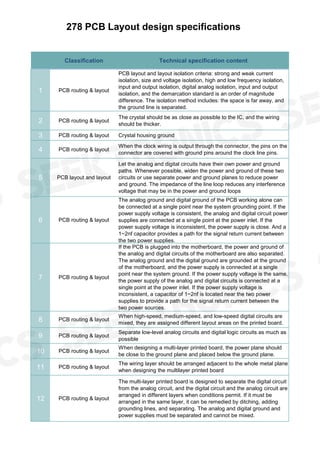
  • 1. 278 PCB Layout design specifications Classification Technical specification content 1 PCB routing & layout PCB layout and layout isolation criteria: strong and weak current isolation, size and voltage isolation, high and low frequency isolation, input and output isolation, digital analog isolation, input and output isolation, and the demarcation standard is an order of magnitude difference. The isolation method includes: the space is far away, and the ground line is separated. 2 PCB routing & layout The crystal should be as close as possible to the IC, and the wiring should be thicker. 3 PCB routing & layout Crystal housing ground 4 PCB routing & layout When the clock wiring is output through the connector, the pins on the connector are covered with ground pins around the clock line pins. 5 PCB layout and layout Let the analog and digital circuits have their own power and ground paths. Whenever possible, widen the power and ground of these two circuits or use separate power and ground planes to reduce power and ground. The impedance of the line loop reduces any interference voltage that may be in the power and ground loops 6 PCB routing & layout The analog ground and digital ground of the PCB working alone can be connected at a single point near the system grounding point. If the power supply voltage is consistent, the analog and digital circuit power supplies are connected at a single point at the power inlet. If the power supply voltage is inconsistent, the power supply is close. And a 1~2nf capacitor provides a path for the signal return current between the two power supplies. 7 PCB routing & layout If the PCB is plugged into the motherboard, the power and ground of the analog and digital circuits of the motherboard are also separated. The analog ground and the digital ground are grounded at the ground of the motherboard, and the power supply is connected at a single point near the system ground. If the power supply voltage is the same, the power supply of the analog and digital circuits is connected at a single point at the power inlet. If the power supply voltage is inconsistent, a capacitor of 1~2nf is located near the two power supplies to provide a path for the signal return current between the two power sources. 8 PCB routing & layout When high-speed, medium-speed, and low-speed digital circuits are mixed, they are assigned different layout areas on the printed board. 9 PCB routing & layout Separate low-level analog circuits and digital logic circuits as much as possible 10 PCB routing & layout When designing a multi-layer printed board, the power plane should be close to the ground plane and placed below the ground plane. 11 PCB routing & layout The wiring layer should be arranged adjacent to the whole metal plane when designing the multilayer printed board 12 PCB routing & layout The multi-layer printed board is designed to separate the digital circuit from the analog circuit, and the digital circuit and the analog circuit are arranged in different layers when conditions permit. If it must be arranged in the same layer, it can be remedied by ditching, adding grounding lines, and separating. The analog and digital ground and power supplies must be separated and cannot be mixed.
  • 2. 13 PCB routing & layout The main requirements of analog circuit to ground wire are integrity, small loop, impedance matching. Digital signals have no special requirements if low frequency; if high speed, impedance matching and ground integrity also need to be considered. 14 PCB routing & layout Clock circuits and high frequency circuits are the main sources of interference and radiation, and must be arranged separately and away from sensitive circuits. 15 PCB routing & layout Pay attention to waveform distortion during long-distance transmission 16 PCB routing & layout To reduce the loop area of the interference source and the sensitive circuit, the best way is to twist the signal line and the ground line (or current-carrying circuit) with twisted pair and shielded wires to make the signal and ground line (or Nearest distance between current carrying loops) 17 PCB routing & layout Increase the distance between the lines so that the mutual inductance between the interferer and the sensed line is as small as possible 18 PCB routing & layout If possible, the line of the interferer is routed at right angles (or near right angles) to the sensed line, which greatly reduces the coupling between the two lines. 19 PCB routing & layout Increasing the distance between lines is the best way to reduce capacitive coupling 20 PCB routing & layout Prior to formal wiring, the first thing to do is to classify the lines. The main classification method is based on the power level and is divided into groups at every 30 dB power level. 21 PCB routing & layout Using blind holes or buried holes is an effective method to increase the density of multilayers, reducing the number of layers and the size of the board and significantly reducing the number of plated through- holes. Through-holes are better and cheaper to implement, so they are generally used in designs 22 PCB routing & layout Wires of different classifications should be bundled separately and laid separately. For adjacent types of wires, they can also be put together after taking measures such as shielding or twisting. The minimum distance between the wire harnesses for sorting is 50~75mm 23 PCB routing & layout In the resistor layout, the gain control resistor and bias resistor (up and down) of the amplifier, pull-up and regulation rectifier circuit should be as close as possible to the amplifier, active device and its power supply and ground to reduce its decoupling effect (improve the transient response). time). 24 PCB routing & layout The bypass capacitor is placed close to the power input 25 PCB routing & layout Decoupling capacitors need to be added in the right place at the right value.For example, add them close to the supply port of your analogue device and you need to use different capacitance values to filter out spurious signals at different frequencies.
  • 3. 26 PCB routing & layout Basic PCB characteristics Impedance: determined by the quality of the copper and cross-sectional area. Specifically: 1 ounce 0.49 milliohms per unit area Capacitance: C=EoErA/h, Eo: free space dielectric constant, Er: PCB substrate dielectric constant, A: current reaching range, h: trace spacing Inductance: average distribution in the wiring, about 1nH / m For ounce copper wire, a 0.5mm wide, 20mm long line above the ground plane can produce 9.8 milliohms of impedance, 20nH of inductance and ground between 0.25mm (10mil) thick FR4 1.66pF coupling capacitor. 27 PCB routing & layout Basic guidelines for PCB layout: increase the trace spacing to reduce the crosstalk of capacitive coupling; arrange the power and ground lines in parallel to optimize the PCB capacitance; place sensitive high frequency lines away from the high noise power line; widen the power supply Line and ground to reduce the impedance of the power and ground lines; 28 PCB routing & layout Segmentation: Physical segmentation to reduce coupling between different types of signal lines, especially power and ground 29 PCB routing & layout Local decoupling: Decoupling the local power supply and the IC, using a large-capacity bypass capacitor between the power input port and the PCB for low-frequency ripple filtering and meeting the burst power requirement, and adopting the power between each IC and the ground. For coupling capacitors, these decoupling capacitors should be as close as possible to the pins. 30 PCB routing & layout Wiring separation: Minimize crosstalk and noise coupling between adjacent lines in the same layer of PCB. The 3W specification is used to handle critical signal paths. 31 PCB routing & layout Protection and shunt lines: measures the two-side grounding protection for key signals and ensure that both ends of the protection line are grounded 32 PCB routing & layout Single-layer PCB: The ground wire should be at least 1.5mm wide, and the jumper and ground line width should be kept to a minimum. 33 PCB routing & layout Double-layer PCB: The ground grid/dot matrix wiring is used preferentially, and the width is maintained at 1.5mm or more. Or put the ground aside and put the signal power on the other side 34 PCB routing & layout Protection ring: use a ground wire to form a ring, and surround the protection logic for isolation. 35 PCB routing & layout PCB Capacitors: PCB capacitors are created on the multilayer board due to the power plane and the thin layer of ground insulation. The advantage is that there is a very high frequency response and a low series inductance that is evenly distributed over the entire surface or the entire line. Equivalent to a decoupling capacitor that is evenly distributed across the board.
  • 4. 36 PCB routing & layout High-speed circuits and low-speed circuits: High-speed circuits should be brought close to the ground plane, and low-speed circuits should be close to the power plane. Copper fill of the ground: Copper fill must be grounded. 37 PCB routing & layout The routing direction of adjacent layers is orthogonal to avoid different signal lines from being in the same direction in adjacent layers to reduce unnecessary interlayer interference; when it is difficult to avoid due to board structure limitations (such as some backplanes) This situation occurs, especially when the signal rate is high, it should be considered to isolate the wiring layers with the ground plane, and isolate the signal lines with the ground signal lines; 38 PCB routing & layout Wiring with one end floating is not allowed, in order to avoid "antenna effect". 39 PCB routing & layout Impedance matching check rule: The wiring width of the same grid should be consistent. The variation of the line width will cause the line characteristic impedance to be uneven. When the transmission speed is high, reflection will occur, which should be avoided in the design. Under certain conditions, variations in line width may not be avoided and the effective length of the inconsistent portion of the middle should be minimized. 40 PCB routing & layout Prevent the signal line from forming a self-loop between different layers, and the self-loop will cause radiation interference. 41 PCB routing & layout Short-term rules: The wiring should be as short as possible, especially for important signal lines, such as clock lines, and keep the oscillator close to the device. 42 PCB routing & layout Chamfer rule: Avoid sharp angles and right angles in PCB design, generate unnecessary radiation, and the process performance is not good. The angle between all lines and lines should be greater than 135 degrees. 43 PCB routing & layout The line connecting the filter capacitor pad to the lands should be connected by a thick line of 0.3mm, and the length of the interconnection should be ≤1.27mm. 44 PCB routing & layout In general, the high frequency part is placed in the interface part to reduce the wiring length. At the same time, we must also consider the segmentation problem of the ground plane in the high/low frequency part. Usually, the ground of the two is divided, and then the single point is connected at the interface. 45 PCB routing & layout For areas with dense vias, care should be taken to avoid interconnecting the power supply and the hollowed out areas of the formation to form a split of the planar layer, thereby destroying the integrity of the planar layer and further increasing the loop area of the signal line in the formation. 46 PCB routing & layout Power layer projection non-overlapping criteria: PCB boards with more than two layers (including), different power layers should avoid overlap in space, mainly to reduce interference between different power supplies, especially between power supplies with large voltage differences. The overlap of the power plane must be avoided. If it is difficult to avoid, consider the middle interval.
  • 5. 47 PCB routing & layout 3W rule: In order to reduce the interference between lines, it should be ensured that the line spacing is large enough. When the line center distance is not less than 3 times the line width, 70% of the electric fields can be kept from interfering with each other. If 98% of the electric fields do not interfere with each other, , 10W rules can be used. 48 PCB routing & layout 20H criterion: With an H (media thickness between power and ground), 70% of the electric field can be confined to the grounding edge if it is 20H, and 98% of the electric field can be confined by 1000H. 49 PCB routing & layout Five-five criteria: printed board layer selection rules, that is, the clock frequency to 5MHZ or pulse rise time is less than 5ns, the PCB board must use multi-layer board, such as the use of double-layer board, it is best to use one side of the printed board as a Complete ground plane 50 PCB routing & layout Mixed-signal PCB zoning guidelines: 1 partition the PCB into separate analog and digital sections; 2 place the A/D converter across the partition; 3 do not divide the ground, and place it uniformly under the analog and digital sections of the board 4 In all layers of the board, the digital signal can only be wired in the digital part of the board, the analog signal can only be wired in the analog part of the board; 5 to achieve analog power and digital power split; 6 wiring can not cross the split power plane The gap between the 7; the signal line that must cross the gap between the divided power sources is located on the wiring layer adjacent to the large area; 8 analyze the path and mode through which the return current actually flows; 51 PCB routing & layout Multilayer boards are a good board level EMC protection design measure and are recommended. 52 PCB routing & layout The signal circuit and the power circuit are independent grounding wires, and finally grounded at one point. They should not have a common grounding wire. 53 PCB routing & layout The signal return ground wire uses a separate low-impedance ground loop, and no chassis or structural frame is used as a loop. 54 PCB routing & layout When the equipment working in the medium and short wave is connected to the earth, the grounding wire is <1/4λ; if the requirement is not met, the grounding wire cannot be an odd multiple of 1/4λ. 55 PCB routing & layout The ground of the strong signal and the weak signal should be arranged separately and connected to the ground network only one point. 56 PCB routing & layout There are at least three separate ground lines in a typical device: one is a low-level circuit ground (called a signal ground), and the other is a relay, a motor, and a high-level circuit ground (called an interference ground or a noise ground). The other is that when the device uses AC power, the safe ground wire of the power supply should be connected to the ground wire of the chassis, and the chassis and the sub-box are insulated, but the two are the same at one point. Finally, all the ground wires are grounded at one point. . The breaker circuit is grounded at a single point at the maximum current point. When f<1MHz, one point is grounded; when f>10MHz, multi-point is grounded; when 1MHz<f<10MHz, if the ground length is <1/20λ, one point is grounded, otherwise multiple points are grounded.
  • 6. 57 PCB routing & layout Avoid ground loop guidelines: Power lines should be routed parallel to ground. 58 PCB routing & layout The heatsink should be connected to the power ground or shielding ground or protective ground in the board (preferably connected to the shielding ground or the protective ground) to reduce the radiation interference. 59 PCB routing & layout Digital ground is separated from analog ground, ground is widened 60 PCB routing & layout Pay attention to different layout areas when mixing high speed, medium speed and low speed 61 PCB routing & layout Dedicated zero-volt line, the trace width of the power line is ≥1mm 62 PCB routing & layout The power and ground wires are as close as possible, and the power and ground on the entire printed board are distributed in a "well" shape to equalize the distribution line current. 63 PCB routing & layout As far as possible, the interference source line and the sense line are wired at right angles 64 PCB routing & layout According to the power classification, the wires of different classifications should be bundled separately, and the distance between the bundles laid separately should be 50-75mm. 65 PCB routing & layout In the case of high requirements, the inner conductor should be provided with a 360° complete package, and the coaxial connector should be used to ensure the integrity of the electric field shielding. 66 PCB routing & layout Multilayer board: The power layer and the ground plane are adjacent. The high speed signal should be close to the ground plane and the non-critical signal should be placed close to the power plane. 67 PCB routing & layout Power: When the circuit requires multiple power supplies, separate each power supply with ground. 68 PCB routing & layout Via: For high speed signals, the via produces an inductance of 1-4nH and a capacitance of 0.3-0.8pF. Therefore, the vias of the high-speed channel should be as small as possible. Make sure that the number of vias on the high-speed parallel lines is the same. 69 PCB routing & layout Short cut: Avoid using stubs on high frequency and sensitive signal lines 70 PCB routing & layout Star signal arrangement: avoiding high speed and sensitive signal lines 71 PCB routing & layout Radiated signal arrangement: Avoid high-speed and sensitive lines, keep the signal path width constant, and do not be too dense through the power supply surface and ground. 72 PCB routing & layout Ground loop area: Keeping the signal path and its ground return line close together will help minimize the ground loop 73 PCB routing & layout Generally, the clock circuit is placed at the center of the PCB or at a well-grounded position, so that the clock is as close as possible to the microprocessor, and the leads are kept as short as possible, and the quartz crystal is oscillated only to the ground of the case.
  • 7. 74 PCB routing & layout Generally, the clock circuit is placed at the center of the PCB or at a well-grounded position, so that the clock is as close as possible to the microprocessor, and the leads are kept as short as possible, and the quartz crystal is oscillated only to the ground of the case. 75 PCB routing & layout The principle of component layout is to divide the analog circuit part from the digital circuit part, divide the high-speed circuit and the low- speed circuit, divide the high-power circuit and the small-signal circuit, divide the noise component and the non-noise component, and minimize the between components. Leads minimize interference with each other. 76 PCB routing & layout The circuit board is divided according to functions, and the ground lines of each partition circuit are connected in parallel with each other and grounded at one point. When there are multiple circuit units on the circuit board, each unit should have independent ground return, each unit is connected to the common ground, and single-panel and double-panel single-point power supply and single-point grounding. 77 PCB routing & layout The important signal lines are as short and thick as possible, and the protective ground is added on both sides. The signals need to be taken out through the flat cable when they are taken out, and the "ground-signal-ground" is used to form a space. 78 PCB routing & layout I/O interface circuit and power drive circuit as close as possible to the edge of the printed board 79 PCB routing & layout In addition to the clock circuit, noise-sensitive devices and circuits are also avoided as much as possible. 80 PCB routing & layout For low frequency signals, it does not matter if there are overholes, for high frequency signals minimize overholes. If there are many lines consider a multi-layer board. 81 PCB routing & layout When there is a high-speed data interface such as PCI or ISA in the printed circuit board period, it is necessary to pay attention to the progressive layout of the signal frequency on the circuit board, that is, the high-frequency circuit, the medium-frequency circuit and the low- frequency circuit are sequentially arranged from the slot interface portion, so that the generation is easy. The disturbing circuitry is remote from the data interface. 82 PCB routing & layout The shorter the lead of the signal on the printed circuit, the longer it should not exceed 25 cm, and the number of vias should be as small as possible. 83 PCB routing & layout When the signal line needs to be turned, use 45 degree or circular arc wiring to avoid using 90 degree polyline to reduce the reflection of high frequency signals. 84 PCB routing & layout Avoid 90 degree fold lines when wiring, reduce high frequency noise emission 85 PCB routing & layout Pay attention to the crystal wiring. The crystal oscillator and the MCU pins are as close as possible. The clock area is isolated by the ground wire. The crystal case is grounded and fixed.
  • 8. 86 PCB routing & layout The board is reasonably partitioned, such as strong and weak signals, digital and analog signals. Keep interference sources (such as motors, relays) and sensitive components (such as microcontrollers) as far as possible 87 PCB routing & layout Use the ground wire to isolate the digital zone from the analog zone, separate the digital ground from the analog ground, and finally connect it to the power ground at one point. A/D and D/A chip wiring are also based on this principle. Manufacturers have considered this requirement when assigning A/D and D/A chip pinouts. 88 PCB routing & layout The ground wire of the MCU and high-power devices should be grounded separately to reduce mutual interference. High-power devices are placed on the edge of the board as much as possible 89 PCB routing & layout Minimize the loop loop area during wiring to reduce induced noise 90 PCB routing & layout When wiring, the power and ground wires should be as thick as possible. In addition to reducing the voltage drop, it is more important to reduce the coupling noise. 91 PCB routing & layout IC devices are soldered directly to the board as much as possible, with fewer IC seats 92 PCB routing & layout The reference point should generally be placed at the intersection of the left and bottom border lines (or the intersection of the extension lines) or the first pad on the board's insert. 93 PCB routing & layout The layout recommends using a 25mil grid 94 PCB routing & layout The total connection is as short as possible and the key signal line is the shortest 95 PCB routing & layout Elements of the same type should be identical in the X or Y direction. The same type of polar discrete components must also strive to be consistent in the X or Y direction for ease of production and commissioning; 96 PCB routing & layout The components should be placed for easy commissioning and maintenance. Small components should not be placed on the side of the large components. There should be sufficient space around the components to be debugged. The heating element should have enough space to facilitate heat dissipation. The thermal element should be kept away from the heating element. 97 PCB routing & layout The distance between the two in-line components is >2 mm. The distance between the BGA and the adjacent device is >5mm. The small components of the resistive and other small components are separated by a distance of 0.7 mm. The outside of the chip component pad and the outside of the adjacent component pad are >2 mm. No plug-in components can be placed within 5 mm of the crimping element. Mounting components should not be placed within 5 mm of the soldering surface. 98 PCB routing & layout The decoupling capacitor of the integrated circuit should be as close as possible to the power supply pin of the chip, and the high frequency is the closest. Make the shortest path between the power supply and the ground.
  • 9. 99 PCB routing & layout The bypass capacitor should be evenly distributed around the integrated circuit. 100 PCB routing & layout When using components, components using the same power supply should be considered as close together as possible for future power splits. 101 PCB routing & layout The placement of the resistive container for impedance matching purposes should be reasonably laid out according to its properties. 102 PCB routing & layout The layout of the matching capacitor resistors should be clearly defined. For multi-load terminal matching, it must be placed at the farthest end of the signal for matching. 103 PCB routing & layout The matching resistor layout should be close to the driving end of the signal, and the distance is generally no more than 500 mils. 104 PCB routing & layout Adjust the characters, all characters can not be above the tray, to ensure that the character information can be clearly seen after the assembly, all characters should be consistent in the X or Y direction. Characters and silk screens must be uniform in size. 105 PCB routing & layout Key signal line priority: priority transmission of key signals such as power supply, analog small signal, high speed signal, clock signal and synchronization signal; 106 PCB routing & layout The minimum rule of the loop: that is, the ring area composed of the signal line and its circuit should be as small as possible, the ring area should be as small as possible, and the smaller the ring area, the less external radiation, and the smaller the interference from the outside. In the double-layer board design, in the case of leaving enough space for the power supply, the remaining part should be filled with the reference ground, and some necessary via holes should be added to effectively connect the double-sided signals, as far as possible for some key signals. Grounding isolation is adopted. For some designs with higher frequencies, special consideration should be given to other planar signal loops. It is recommended to use multi-layer boards. 107 PCB routing & layout Shortest guidelines for grounding leads: Minimize and thicken the grounding leads (especially high frequency circuits). For circuits operating at different levels, long common ground lines are not available. 108 PCB routing & layout In the multi-layer board layout, because the power and ground layers are on the inner layer, we should pay attention not to have the suspended ground plane or the power plane. And also make sure that the overholes punched into the ground are indeed connected to the ground plane, and are to add some test points for some important signals to facilitate measurements during debugging. 109 PCB routing & layout If the internal circuit is to be connected to the metal case, use a single point ground to prevent the discharge current from flowing through the internal circuit.
  • 10. 110 PCB routing & layout Components that are sensitive to electromagnetic interference should be shielded from components or lines that can generate electromagnetic interference. If such lines must pass by the part, they should be used at an angle of 90°. 111 PCB routing & layout If you want to use an LDO to provide power for digital and analog, it is recommended to connect the analog power first. After the analog power is filtered by LC, it becomes the digital power. 112 PCB routing & layout The wiring layer should be arranged adjacent to the entire metal plane. This arrangement is to generate flux cancellation 113 PCB routing & layout There are many loops between the grounding points. The diameter (or grounding point spacing) of these loops should be less than 1/20 of the highest frequency wavelength. 114 PCB routing & layout The power cable and ground wire of single or double panel should be as close as possible. The best way is to connect the power cable to one side of the printed board, and the ground wire is on the other side of the printed board. The impedance is the lowest 115 PCB routing & layout Signal traces (especially high frequency signals) should be as short as possible 116 PCB routing & layout The distance between the two conductors shall comply with the provisions of the electrical safety design specification. The voltage difference shall not exceed the breakdown voltage of the air and the insulating medium between them, otherwise an arc will be generated. In the 0.7ns to 10ns time, the arc current can reach tens of A, and sometimes even exceed 100 amps. The arc will remain until the two conductors are shorted or the current is low enough to sustain the arc. Examples of possible spikes are hand or metal objects, which are identified during design. 117 PCB routing & layout Add a ground plane immediately adjacent the double panel and connect the ground plane to the ground point on the circuit at the shortest spacing. 118 PCB routing & layout Make sure that each cable entry point is within 40mm (1.6 inches) of the chassis ground. 119 PCB routing & layout Connect the connector housing and the metal switch housing to the chassis ground. 120 PCB routing & layout Place a wide conductive guard ring around the membrane keyboard, attach the outer perimeter of the ring to the metal chassis, or connect to the metal chassis at least at the four corners. Do not connect the guard ring to the PCB ground. 121 PCB routing & layout Use of multi-layer PCB: Compared to double-sided PCB, ground plane and power plane and tightly spaced signal line-ground spacing can reduce common impedance and inductive coupling to achieve double- sided PCB /10 to 1/100. Try to keep each signal layer close to a power or ground plane.
  • 11. 122 PCB routing & layout For high-density PCBs with components on the top and bottom surfaces, short traces, and lots of fill, the inner trace can be used. Most of the signal lines, as well as the power and ground planes, are on the inner layer and are therefore similar to Faraday boxes with shielding. 123 PCB routing & layout Place all connectors on the side of the board as much as possible. 124 PCB routing & layout Place a wide chassis ground or polygon fill on all PCB layers underneath the connector (which is easily hit directly by the ESD) and connect them with vias every 13mm. 125 PCB routing & layout When assembling the PCB, do not apply any solder to the top or bottom mounting hole pads. Use a screw with an inset washer to make the PCB in close contact with the metal chassis/shield or ground plane bracket. 126 PCB routing & layout The same "isolation zone" should be placed between the chassis ground and circuit ground of each layer; if possible, keep the separation distance 0.64 mm (0.025 inch). 127 PCB routing & layout A circular ring is placed around the circuit to prevent ESD interference: 1 put a circular path on the entire circumference of the board; 2 the annular width of all layers is >2.5mm (0.1 inch); 3 every 13mm (0.5 inch) with a via hole Connected together; 4 connects the ring ground to the common ground of the multilayer circuit; 5 pairs of double panels installed in the metal chassis or shielding device should be connected to the circuit publicly; 6 unshielded The double-sided circuit is connected annularly to the chassis ground, and no solder resist is applied annularly so that the annular discharge can act as a discharge rod for the ESD, at least one 0.5 mm wide at a position on the annular ground (all layers) ( 0.020") gap to avoid large ground loops; 7 If the board is not placed in a metal chassis or shield, solder resists should not be applied to the top and bottom chassis grounds of the board so they can be used as ESD A discharge rod for an electric arc. 128 PCB routing & layout In the area that can be directly hit by ESD, a ground line is placed near each signal line. 129 PCB routing & layout Circuits that are susceptible to ESD are placed in the middle of the PCB to reduce the likelihood of being touched. 130 PCB routing & layout When the length of the signal line is greater than 300mm (12 inches), be sure to lay a ground wire in parallel. 131 PCB routing & layout Connection guidelines for mounting holes: can be connected to or isolated from the circuit. 1 When the metal bracket must be used with a metal shield or chassis, a 0Ω resistor is used for the connection. 2. Determine the mounting hole size to achieve reliable mounting of the metal or plastic bracket. Large pads should be used on the top and bottom of the mounting holes. Solder resists should not be used on the bottom pads, and the underlying pads should not be soldered by wave soldering.
  • 12. 132 PCB routing & layout Protected signal lines and unprotected signal lines are prohibited from being arranged in parallel. 133 PCB routing & layout Wiring guidelines for reset, interrupt, and control signal lines: 1 using high frequency filtering; 2 away from the input and output circuits; 3 away from the edge of the board. 134 PCB routing & layout The boards inside the chassis are not installed in the open position or at the internal seams. 135 PCB routing & layout The most sensitive circuit board for static electricity is placed in the middle, where it is not easily accessible by humans; the static- sensitive components are placed in the middle of the board and are not easily accessible by humans. 136 PCB routing & layout Binding criteria between two metal blocks: 1 solid bonding tape is better than woven bonding tape; 2 bonding is not wet without water; 3 using multiple conductors to ground the ground plane of all boards in the chassis Or the ground grids are connected together; 4 ensure that the width of the bonding points and washers is greater than 5 mm. 137 Circuit design Signal Filter Leg Coupling: For each analog amplifier power supply, a decoupling capacitor must be added between the amplifiers closest to the circuit connection. For digital integrated circuits, add decoupling capacitors in groups. A capacitor bypass is installed on the brush of the motor and the generator, and an R-C filter is connected in series on each winding branch, and low-pass filtering is added at the power inlet to suppress interference. Install the filter as close as possible to the device being filtered, using short, shielded leads as the coupling medium. All filters must be shielded and the input and output leads should be isolated. 138 Circuit design Each function board clarifies the voltage fluctuation range, ripple, noise, load adjustment rate, etc. of the power supply. The secondary power supply must meet the above requirements when it reaches the function board. 139 Circuit design A circuit with radiation source characteristics is placed within the metal shield to minimize transient interference. 140 Circuit design Add a protection device at the cable entrance 141 Circuit design Each IC's power supply pin should be connected with a bypass capacitor (typically 104) and a smoothing capacitor (10uF~100uF) to ground. The power supply pins of each corner of the large-area IC should also be supplied with bypass capacitors and smoothing capacitors. 142 Circuit design Impedance mismatch criteria for filter selection: For low impedance noise sources, the filter needs to be high impedance (large series inductance); for high impedance noise sources, the filter needs to be low impedance (large parallel capacitance) 143 Circuit design Capacitor housing, auxiliary lead-out terminals must be completely isolated from the positive and negative terminals and the board
  • 13. 144 Circuit design The filter connector must be well grounded and the metal case filter grounded. 145 Circuit design All pins of the filter connector are filtered 146 Circuit design The electromagnetic compatibility design of digital circuits is to consider the frequency bandwidth determined by the rising and falling edges of the digital pulse rather than the repetition frequency of the digital pulse. The printed circuit board design bandwidth of a square digital signal is set to 1/πtr, usually taking into account the bandwidth of this bandwidth. 147 Circuit design Using R-S flip-flops as a buffer between the device control buttons and the device electronics 148 Circuit design Reducing the input impedance of sensitive lines effectively reduces the likelihood of introducing interference. 149 Circuit design LC Filter An LC filter is required between the low output impedance power supply and the high impedance digital circuit to ensure impedance matching of the loop. 150 Circuit design Voltage calibration circuit: At the input and output terminals, a decoupling capacitor (such as 0.1μF) is added, and the bypass capacitor selection value follows the standard of 10μF/A. 151 Circuit design Signal Termination: Impedance matching between the source and destination of the high frequency circuit is very important, and incorrect matching leads to signal feedback and damped oscillation. Excessive RF energy can cause EMI problems. At this point, you need to consider signal termination. There are several types of signal terminations: series/source termination, parallel termination, RC termination, Thevenin termination, diode termination. 152 Circuit design MCU circuit: I/O pin: The vacant I/O pin is connected to a high impedance to reduce the supply current. And avoid floating. IRQ pin: There should be measures to prevent electrostatic discharge on the IRQ pin. For example, using bidirectional diodes, Transorbs or metal oxide varistor. Reset pin: The reset pin has a time delay. In order to avoid the initial reset of the MCU. Oscillator: The lower the clock oscillation frequency used by the MCU, the better, if the requirements are met. Let the clock circuit, calibration circuit and decoupling circuit be placed close to the MCU 153 Circuit design A small-scale integrated circuit with less than 10 outputs, with a working frequency of ≤ 50 MHz, at least one 0.1 uf filter capacitor. When the operating frequency is ≥50MHZ, each power supply pin is connected with a 0.1uf filter capacitor;
  • 14. 154 Circuit design For medium to large scale integrated circuits, each power supply pin is mated with a 0.1uf filter capacitor. For circuits with large power supply redundancy, the number of matching capacitors can be calculated according to the number of output pins, and a 0.1uf filter capacitor is connected to every 5 outputs. 155 Circuit design For a region without active devices, connect at least one 0.1uf filter capacitor per 6cm2 156 Circuit design For UHF circuits, each power supply pin is mated with a 1000pf filter capacitor. For circuits with large power supply redundancy, the number of matching capacitors can be calculated according to the number of output pins, and a 1000pf filter capacitor is connected to every 5 outputs. 157 Circuit design The high frequency capacitor should be as close as possible to the power supply pin of the IC circuit. 158 Circuit design At least one 0.1uf filter capacitor is connected to every 5 high frequency filter capacitors; 159 Circuit design Each 5 10uf is equipped with at least two 47uf low frequency filter capacitors; 160 Circuit design At least one 220uf or 470uf low frequency filter capacitor is connected every 100cm2; 161 Circuit design At least 2 220uf or 470uf capacitors should be placed around the power outlet of each module. If space permits, the number of capacitors should be appropriately increased. 162 Circuit design Pulse and transformer isolation criteria: The pulse network and the transformer must be isolated. The transformer can only be connected to the decoupling pulse network with the shortest connection line. 163 Circuit design In the process of opening and closing the switch and the closet, in order to prevent arc interference, a simple RC network, an inductive network can be connected, and a high resistance, a rectifier or a load resistor is added to these circuits, and if not, Shield the input and output leads. In addition, a feedthrough capacitor can be connected to these circuits. 164 Circuit design The decoupling and filter capacitors must be analyzed according to the high frequency equivalent circuit diagram. 165 Circuit design Appropriate filter circuits should be used for the introduction of power supply for each function board. The differential mode noise and common mode noise should be filtered out at the same time. The noise discharge ground should be separated from the working ground, especially the signal ground. Consider using the protection ground; Decoupling capacitors should be placed at the input of the power supply to improve anti-interference ability
  • 15. 166 Circuit design Defining the maximum operating frequency of each board and taking necessary shielding measures for devices or components with an operating frequency above 160MHz (or 200 MHz) to reduce the level of radiated interference and improve the ability to resist radiation interference. 167 Circuit design If possible, add R-C decoupling at the entrance of the control line (on the printed board) to eliminate possible interference factors in the transmission. 168 Circuit design Using R-S flip-flops to buffer the cooperation between buttons and electronic circuits 169 Circuit design Use a fast recovery diode in the secondary rectification loop or a polyester film capacitor in parallel with the diode 170 Circuit design “Trimming” the transistor switching waveform 171 Circuit design Reduce the input impedance of sensitive lines 172 Circuit design If it is possible to use a balanced line as input in the sensitive circuit, the common mode rejection capability inherent in the balanced line can be used to overcome the interference of the interference source to the sensitive line. 173 Circuit design The way to ground the load directly is not appropriate 174 Circuit design Note that bypass decoupling capacitors (typically 104) are added between the power supply and ground at the near end of the IC. 175 Circuit design If possible, the sensitive circuit uses a balanced line for input and the balanced line is not grounded. 176 Circuit design The relay coil adds a freewheeling diode to eliminate back EMF interference when the coil is disconnected. Only the freewheeling diode will delay the opening time of the relay. After the Zener diode is added, the relay can move more times per unit time. 177 Circuit design Spark suppression circuit is connected at both ends of the relay contact (generally RC series circuit, the resistance is generally selected from a few K to tens of K, and the capacitor is selected as 0.01uF) to reduce the influence of spark 178 Circuit design Add a filter circuit to the motor, pay attention to the capacitor and inductor leads as short as possible 179 Circuit design Each IC on the board should be connected with a high-frequency capacitor of 0.01μF to 0.1μF to reduce the impact of the IC on the power supply. Pay attention to the wiring of high-frequency capacitors. The wiring should be close to the power supply terminal and be as short and as short as possible. Otherwise, it will increase the equivalent series resistance of the capacitor and affect the filtering effect.
  • 16. 180 Circuit design The RC suppression circuit is connected to both ends of the thyristor to reduce the noise generated by the thyristor (this thyristor may break down when this noise is severe) 181 Circuit design Many single-chip microcomputers are very sensitive to power supply noise. It is necessary to add a filter circuit or a voltage regulator to the power supply of the single-chip microcomputer to reduce the interference of the power supply noise on the single-chip microcomputer. For example, a magnetic bead and a capacitor can be used to form a π-shaped filter circuit. Of course, when the condition is not high, a 100Ω resistor can be used instead of the magnetic bead. 182 Circuit design If the I/O port of the microcontroller is used to control noise devices such as motors, isolation should be added between the I/O port and the noise source (increasing the π-shaped filter circuit). Control noise devices such as motors, and add isolation between the I/O port and the noise source (increasing the π-shaped filter circuit). 183 Circuit design Use anti-interference components such as magnetic beads, magnetic rings, power filters, and shields in key areas such as I/O ports, power lines, and circuit board connectors. This can significantly improve the anti-jamming performance of the circuit. 184 Circuit design For the idle I/O port of the MCU, do not hang it, ground it or connect it to the power supply. The idle ends of other ICs are grounded or connected to the power supply without changing the system logic. 185 Circuit design Power supply monitoring and watchdog circuits for single-chip microcomputers, such as IMP809, IMP706, IMP813, X25043, X25045, etc., can greatly improve the anti-interference performance of the entire circuit. 186 Circuit design Under the premise that the speed can meet the requirements, try to reduce the crystal oscillator of the single-chip microcomputer and select the low-speed digital circuit. 187 Circuit design If possible, add RC low-pass filters or EMI suppression components (such as magnetic beads, signal filters, etc.) to the interface of the PCB to eliminate interference from the cable; however, be careful not to affect the transmission of useful signals. 188 Circuit design Clock output wiring should not be directly connected to multiple components (called daisy-chain connection); instead, the clock should be directly provided to other components via the buffer. 189 Circuit design Extend the membrane keyboard border to 12mm beyond the wire, or use a plastic cut to increase the path length. 190 Circuit design Near the connector, connect the signal on the connector to the chassis ground of the connector with an L-C or bead-capacitor filter. 191 Circuit design Add a magnetic bead between the chassis ground and the circuit common ground.
  • 17. 192 Circuit design The power distribution system inside the electronic device is the main object of the ESD arc inductive coupling. The power distribution system is anti-ESD measures: 1 tightly twisting the power line and the corresponding return line; 2 entering the electronic device in each power line Place a magnetic bead; 3 Place a transient suppressor, metal oxide varistor (MOV) or 1kV high frequency capacitor between each power supply pin and the ground of the electronics chassis; 4 is best placed on the PCB Dedicated power and ground planes, or tight power and ground grids with a large number of bypass and decoupling capacitors. 193 Circuit design Place resistors and beads in series on the receiving end. For cable drivers that are easily hit by ESD, you can also place resistors or beads in series on the drive end. 194 Circuit design Place a transient protector on the receiving end. 1 Connect to the chassis ground with a short, thick wire (less than 5 times the width, preferably less than 3 times the width). 2 The signal and ground wires coming out of the connector should be connected directly to the transient protector before they can be connected to other parts of the circuit. 195 Circuit design A filter capacitor is placed at the connector or within 25 mm (1.0 inch) of the receiving circuit. 1 Use a short, thick wire to connect to the chassis ground or receive circuit ground (length less than 5 times the width, preferably less than 3 times the width). 2 The signal line and the ground line are first connected to the capacitor and then connected to the receiving circuit. 196 Casing On the metal chassis, the maximum diameter of the opening is ≤ λ/20, λ is the wavelength of the highest frequency electromagnetic wave inside and outside the machine; the non-metal chassis is regarded as unprotected in the electromagnetic compatibility design. 197 Casing The number of seams of the shield is the least; the joint of the shield has a good electrical continuity; the venting hole D<3mm, this aperture can effectively avoid large electromagnetic leakage or entry; shielding opening Where (such as vents) are sealed with a thin copper mesh or other suitable conductive material; if the vent metal mesh is to be removed frequently, it can be fixed around the hole with screws or bolts, but the screw spacing is <25mm to maintain continuous line contact. 198 Casing f>1MHz, 0.5mm thick metal plate shield, the field strength is reduced by 99%; when f>10MHz, 0.1mm copper shield reduces the field strength by more than 99%; f>100MHz, the surface of the insulator is plated A copper layer or a silver plated layer is a good shield. However, it should be noted that for the plastic Casing, when the metal coating is sprayed inside, the domestic spraying process is not closed, the continuous conduction effect between the coating particles is not good, and the conduction resistance is large, and the negative effect of the coating may be emphasized.
  • 18. 199 Casing The joint of the whole machine protection ground is not coated with insulating varnish. It is necessary to ensure reliable metal contact with the protective earth cable, and avoid the wrong way of relying only on the screw thread for grounding connection. 200 Casing Establish a complete shield structure with a grounded metal shielded housing that discharges discharge current to ground 201 Casing Establish an anti-ESD environment with a breakdown voltage of 20kV; measures to increase the distance are effective. 202 Casing The length of the path between the electronic equipment and the following items exceeds 20 mm, including the seams, vents, and mounting holes, and any unusable metal that can be accessed by user operators, such as fasteners, switches, Joystick and indicator. 203 Casing The seams and mounting holes are covered with a mylar film in the chassis, which extends the edges of the seams/vias and increases the path length. 204 Casing Cover the unused or rarely used connectors with metal caps or shielded plastic dust caps. 205 Casing Use a switch with a plastic shaft and a joystick, or place a plastic handle/sleeve on top to increase the path length. Avoid using handles with metal fixing screws. 206 Casing Install the LEDs and other indicators in the holes in the device and cover them with a strap or cover to extend the edge of the hole or use a conduit to increase the path length. 207 Casing Place the heat sink close to the seam of the chassis, and the sides and corners on the metal parts of the vent or mounting hole should be rounded. 208 Casing In plastic cases, metal fasteners that are close to the electronics or that are not grounded cannot protrude into the chassis. 209 Casing High support feet keep the device away from the table or floor to solve indirect ESD coupling problems on the desktop/ground or horizontal coupling surfaces. 210 Casing Apply an adhesive or sealant around the membrane keyboard circuit layer. 211 Casing Chassis Bonding Point and Edge Protection Guidelines: Bonding points and edges are critical. At the junction of the chassis, high- pressure silicone or gaskets are used to achieve hermetic, ESD-proof, waterproof and dust-proof. 212 Casing An ungrounded chassis should have a breakdown voltage of at least 20kV (rules A1 through A9); for a grounded chassis, the electronic device must have at least a breakdown voltage of 1500V to prevent secondary arcing, and a path length of 2.2 mm or more is required.
  • 19. 213 Casing The chassis is made of the following shielding materials: metal plate; polyester film/copper or polyester film/aluminum plate; thermoformed metal mesh with welded joints; thermoformed metallized fiber mat (non-woven) or fabric (woven); Silver, copper or nickel coating; zinc arc spraying; vacuum metal treatment; electroless plating; adding conductor filling material to plastic; 214 Casing Anti-electrochemical corrosion criteria for shielding materials: The potential of the components in contact with each other (EMF) < 0.75V. If in a salty, humid environment, the potential between them must be <0.25V. The size of the anode (positive) component should be larger than the cathode (negative) component. 215 Casing A shielding material having a slit width of 5 times or more is laminated on the joint. 216 Casing The electrical connection is made by welding, fasteners, etc. at a distance of 20 mm (0.8 inch) between the shield layer and the case. 217 Casing The gap is bridged by a gasket to eliminate grooving and provide a conductive path between the slits. 218 Casing Avoid straight corners and excessive corners in the shielding material. 219 Casing The aperture is ≤ 20 mm and the length of the groove is ≤ 20 mm. Under the same opening area condition, the opening is preferred instead of the slotting. 220 Casing If possible, replace the large opening with a few small openings, with the spacing between the openings as large as possible. 221 Casing For grounded equipment, connect the shield to the chassis ground where the connector enters; for ungrounded (double isolated) equipment, connect the shield material to the circuit near the switch. 222 Casing Whenever possible, let the cable entry point near the center of the panel, not near the edge or corner. 223 Casing The individual slots arranged in the shielding device are parallel and not perpendicular to the direction in which the ESD current flows. 224 Casing Use a metal plate with a metal bracket to act as an additional grounding point at the location of the mounting holes, or use a plastic bracket for insulation and isolation. 225 Casing Install a partial shield at the control panel and keyboard location on the plastic chassis to block ESD: 226 Casing The location of the power connector and the connector leading to the outside is to be connected to the chassis ground or to the circuit common ground. 227 Casing Polyester film/copper or polyester film/aluminum platens are used in plastics, or conductive coatings or conductive fillers are used. 228 Casing A thin conductive chrome plating or chromate coating is used on the aluminum plate, but anodization cannot be used. 229 Casing Conductive filler materials are used in plastics. Note that the surface of the molded part usually has a resin material, and it is difficult to achieve a low-resistance connection. 230 Casing A thin conductive chromate coating is used on the steel material.
  • 20. 231 Casing The clean, neat metal surfaces are in direct contact without relying on screws to achieve the connection of the metal parts. 232 Casing A shield coating (indium tin oxide, indium oxide, tin oxide, etc.) is used to connect the display to the chassis shield along the entire periphery. 233 Casing At the location where the operator is often in contact, provide an antistatic (weak conductive) path to the ground, such as the space bar on the keyboard. 234 Casing It is difficult for the operator to generate an arc discharge to the edge or corner of the metal sheet. Arcing to these points will cause more indirect ESD effects than arcing to the center of the metal plate. 235 Others The shielding protection criteria of the display window: 1 install a shielded protective window; 2 the external circuit part and the circuit connection in the machine are connected by a filter component. 236 Others Key window protection guidelines: 237 Component selection The capacitor should be selected as much as possible for the chip capacitor, and the lead inductance is small. 238 Component selection Stable power supply bypass capacitor, choose electrolytic capacitor 239 Component selection Capacitors for AC coupling and charge storage are selected from polytetrafluoroethylene capacitors or other polyester (polypropylene, polystyrene, etc.) capacitors. 240 Component selection Monolithic ceramic capacitor for high frequency circuit decoupling 241 Component selection The criteria for capacitor selection are: As low as possible ESR capacitors; The resonant frequency value of the capacitor as high as possible; 242 Component selection Aluminum electrolytic capacitors should be avoided in the following situations: a, high temperature (temperature exceeds the maximum operating temperature) b. Overcurrent (current exceeds the rated ripple current). When the applied ripple current exceeds the rated value, the capacitor body will overheat, the capacity will decrease, and the life will be shortened. c. Overvoltage (voltage exceeds rated voltage). When the voltage applied to the capacitor is higher than the rated working voltage, the leakage current of the capacitor will rise and its oxygen property will deteriorate in a short period of time until it is damaged. d. Apply reverse voltage or AC voltage. When the value flow aluminum electrolytic capacitor is connected to the circuit in reverse polarity, the capacitor will cause the electronic circuit to be short- circuited, and the resulting current will cause damage to the capacitor. If it is possible to apply a positive voltage to the negative lead in the circuit, please select a non-polar product. e. Used in circuits that repeatedly charge and discharge abruptly, when a conventional capacitor is used for fast charging. Its service life may be reduced due to a decrease in capacity and a sharp rise in temperature.
  • 21. 243 Component selection It is only necessary to use a filter connector on the shielded chassis. 244 Component selection When selecting a filter connector, in addition to the factors to be considered when selecting a normal connector, the cutoff frequency of the filter should also be considered. When the frequency of the signal transmitted on each core wire in the connector is different, the cutoff frequency is determined based on the signal with the highest frequency. 245 Component selection Package select SMT as much as possible 246 Component selection The choice of the preferred carbon film for the resistor, and the second metal film, when selecting the wire winding for power reasons, must consider the inductance effect 247 Component selection Capacitor selection should pay attention to aluminum electrolytic capacitors, tantalum electrolytic capacitors for low frequency terminals; ceramic capacitors for medium frequency range (from KHz to MHz); ceramic and mica capacitors for VHF and microwave circuits; try to use low ESR (etc. 248 Component selection The bypass capacitor selects the electrolytic capacitor, and the capacitance value is 10-470PF, which depends mainly on the transient current demand on the PCB. 249 Component selection The decoupling capacitor should be a ceramic capacitor with a capacitance of 1/100 or 1/1000 of the bypass capacitor. It depends on the rise and fall times of the fastest signal. For example, 100MHz takes 10nF, 33MHz takes 4.7-100nF, And the ESR value is less than 1 ohm. Select NPO for decoupling above 50MHz, Z5U for low frequency decoupling, preferably for parallel decoupling of capacitors with two orders of magnitude difference 250 Component selection When the inductor is selected, the closed loop is better than the open loop, and the open loop is better than the rod or solenoid. Select ferromagnetic core for low frequency applications, select ferrite core for high frequency applications 251 Component selection Ferrite Beads High Frequency Attenuation 10dB 252 Component selection Ferrite clamp common mode (CM) and differential mode (DM) attenuation in the MHz frequency range up to 10-20dB 253 Component selection Diode selection: Schottky diodes: for fast transient signals and sharp pulse protection; Zener diode: for ESD (electrostatic discharge) protection; overvoltage protection; low capacitance and high data rate signal protection Transient Voltage Suppression Diode (TVS): ESD excitation transient high voltage protection, instantaneous spike reduction Varistor diode: ESD protection; high voltage and high transient protection 254 Component selection TVS tubes and fuses are a must for power supplies. In the case of signals, TVS tubes and diodes must be added to protect the analogue circuit input from large voltages.
  • 22. 255 Component selection integrated circuit: The choice of CMOS devices, especially high-speed devices, has dynamic power requirements that require decoupling to meet their instantaneous power requirements. 256 Component selection In high-frequency environments, the pin will form an inductor with a value of approximately 1nH/1mm, and the end of the pin will also have a small capacitive effect backwards, approximately 4pF. Surface- mount devices facilitate EMI performance with parasitic inductance and capacitance values of 0.5nH and 0.5pF, respectively. 257 Component selection Radial pins are superior to axial parallel pins; 258 Component selection TTL and CMOS hybrid circuits generate clocks, useful signals, and power supply harmonics because of different switch hold times, so it is best to choose the same series of logic circuits. 259 Component selection Unused CMOS device pins must be grounded or connected to a power supply through a series resistor. 260 Component selection The rated current of the filter is 1.5 times the actual operating current value. 261 Component selection Selection of power filter: According to theoretical calculation or test result, the insertion loss value of the power supply filter should be IL. In actual selection, the power supply filter with the insertion loss of IL+20dB should be selected. 262 Component selection The AC filter and the tributary filter are not replaceable in the actual product. In the temporary prototype, the AC filter can be used to temporarily replace the DC filter; however, the DC filter is absolutely not available for AC, DC filter to ground capacitance. The filter cutoff frequency is low and the AC current will cause a large loss on it. 263 Component selection Avoid using static sensitive devices. The electrostatic sensitivity of the selected device is generally not less than 2000V. Otherwise, it is necessary to carefully evaluate and design an antistatic method. In terms of structure, it is necessary to achieve good ground gas connection and take necessary insulation or shielding measures to improve the antistatic ability of the whole machine. 264 Component selection With shielded twisted pair, the signal current flows on the two inner conductors, and the noise current flows in the shield, thus eliminating the coupling of the common impedance, and any interference will be induced on both conductors simultaneously, so that the noise is cancelled. 265 Component selection Unshielded twisted pairs have less ability to withstand electrostatic coupling. But it still plays a very good role in preventing magnetic field induction. The shielding effect of the unshielded twisted pair is proportional to the number of twists per unit length of the wire. 266 Component selection Coaxial cables have a relatively uniform characteristic impedance and low loss, making them better from DC to VHF. 267 Component selection Do not use high-speed logic circuits wherever high-speed logic circuits can be used.
  • 23. 268 Component selection When selecting a logic device, try to select a device with a rise time longer than 5ns, and do not select a logic device that requires faster timing than the circuit. 269 System When multiple devices are connected to an electrical system, in order to eliminate the interference caused by the ground loop power supply, isolation transformers, neutralization transformers, optocouplers, and differential amplifier common mode inputs are used for isolation. 270 System Identify the interference device and the interference circuit: in the start-stop or running state, the device or circuit with a voltage change rate dV/dt and a current rate of change di/dt is an interference device or an interference circuit. 271 System A grounded conductive layer is placed between the membrane keyboard circuit and its adjacent circuitry. 272 Cables and connectors PCB layout and layout isolation criteria: strong and weak current isolation, size and voltage isolation, high and low frequency isolation, input and output isolation, digital analog isolation, input and output isolation, and the demarcation standard is an order of magnitude difference. The isolation method includes: shielding one or all of the independent shielding, space away, and ground separation. 273 Cables and connectors Unshielded ribbon cable. The best way to connect is between the signal and the ground. The next method is to push one ground, two signals, and so on, or a dedicated grounding plate. 274 Cables and connectors Signal Cable Shielding Guidelines: 1 Strong interference signal transmission uses twisted pair or dedicated externally shielded twisted pair. 2 DC power line application shielded line; 3 AC power line application twisted wire; 4 All signal lines/power lines entering the shielded area must be filtered. 5 All shielded wires (sets) should have good contact with the ground at both ends. As long as no harmful ground loops are generated, all cable shields should be grounded at both ends. For very long cables, there should be grounding points in the middle. 6 In sensitive low-level circuits, to eliminate possible interference in the ground loop, each circuit should have its own isolation and shielding ground wire. 275 Cables and connectors The shielded wire is in close contact with the metal base plate. All cables with shielding should be placed close to the metal plate to prevent the magnetic field from passing through the circuit formed by the metal floor and the shield wire. 276 Cables and connectors The plug of the printed circuit should also arrange some zero-volt lines as the line isolation. 277 Cables and connectors The best way to reduce the loop area of interference and sensitive circuits is to use twisted pair and shielded wires. 278 Cables and connectors Twisted pair is very effective at less than 100KHz, and is limited at high frequencies due to uneven characteristic impedance and resulting waveform reflection.