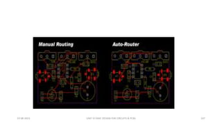
SlideShare a Scribd company logo
1 of 136
UNIT IV
EMC DESIGN FOR CIRCUITS
AND PCBS
Prepared by
Mrs.R.Ponni , AP / ECE
SYLLABUS
UNIT IV
EMC DESIGN FOR CIRCUITS AND PCBS 9
Noise from Relays and Switches; Nonlinearities in Circuits; Cross
talk in transmission line and cross talk control; Component selection
and mounting; PCB trace impedance; Routing; Power distribution
decoupling; Zoning; Grounding; VIAs; Terminations.
UNIT IV EMIC DESIGN FOR CIRCUITS & PCBS 2
19-08-2023
19-08-2023 UNIT IV EMIC DESIGN FOR CIRCUITS & PCBS 3
19-08-2023 UNIT IV EMIC DESIGN FOR CIRCUITS & PCBS 4
19-08-2023 UNIT IV EMIC DESIGN FOR CIRCUITS & PCBS 5
19-08-2023 UNIT IV EMIC DESIGN FOR CIRCUITS & PCBS 6
19-08-2023 UNIT IV EMIC DESIGN FOR CIRCUITS & PCBS 7
19-08-2023 UNIT IV EMIC DESIGN FOR CIRCUITS & PCBS 8
19-08-2023 UNIT IV EMIC DESIGN FOR CIRCUITS & PCBS 9
19-08-2023 UNIT IV EMIC DESIGN FOR CIRCUITS & PCBS 10
19-08-2023 UNIT IV EMIC DESIGN FOR CIRCUITS & PCBS 11
19-08-2023 UNIT IV EMIC DESIGN FOR CIRCUITS & PCBS 12
19-08-2023 UNIT IV EMIC DESIGN FOR CIRCUITS & PCBS 13
19-08-2023 UNIT IV EMIC DESIGN FOR CIRCUITS & PCBS 14
19-08-2023 UNIT IV EMIC DESIGN FOR CIRCUITS & PCBS 15
19-08-2023 UNIT IV EMIC DESIGN FOR CIRCUITS & PCBS 16
19-08-2023 UNIT IV EMIC DESIGN FOR CIRCUITS & PCBS 17
19-08-2023 UNIT IV EMIC DESIGN FOR CIRCUITS & PCBS 18
19-08-2023 UNIT IV EMIC DESIGN FOR CIRCUITS & PCBS 19
19-08-2023 UNIT IV EMIC DESIGN FOR CIRCUITS & PCBS 20
19-08-2023 UNIT IV EMIC DESIGN FOR CIRCUITS & PCBS 21
19-08-2023 UNIT IV EMIC DESIGN FOR CIRCUITS & PCBS 22
PCB Trace Impedance
19-08-2023 UNIT IV EMIC DESIGN FOR CIRCUITS & PCBS 24
19-08-2023 UNIT IV EMIC DESIGN FOR CIRCUITS & PCBS 25
19-08-2023 UNIT IV EMIC DESIGN FOR CIRCUITS & PCBS 26
PCB Trace:
• It is a running path of copper on a printed circuit board. Through
the traces, current can travel to different areas of the printed
circuit board where the components are placed so that the
desired action can be performed
• Traces on PCB
• Traces are usually of two main type i.e. small and large trace.
1.Small Trace: A small trace on a Printed Circuit Board connects
the Reset pad to any other part of the printed circuit board.
2.Large Trace: It connects the components to the 5V power pin.
19-08-2023 UNIT IV EMIC DESIGN FOR CIRCUITS & PCBS 27
19-08-2023 UNIT IV EMIC DESIGN FOR CIRCUITS & PCBS 28
Near magnetic field above a packaged
integrated circuit.
19-08-2023 UNIT IV EMIC DESIGN FOR CIRCUITS & PCBS 29
• What is Impedance?
• Impedance is the combination of the capacitance and
inductance of a circuit when operated at high frequency.
Though also measured in Ohms, it is somewhat different than
resistance which is a DC characteristic. Impedance is an AC
characteristic, meaning that it is related to frequency, resistance
is not.
19-08-2023 UNIT IV EMIC DESIGN FOR CIRCUITS & PCBS 30
About trace:
1.Every trace has series inductance.
2.It is distributed along the trace and is inversely related to the
cross-sectional area of the trace.
3.It is admittedly small, but it is non-zero.
4.Therefore, for fast enough rise times, the impedance it offers
can be significant.
19-08-2023 UNIT IV EMIC DESIGN FOR CIRCUITS & PCBS 31
• Every trace has capacitance between the trace and the return
path of the signal on the trace, wherever that return path might
be.
• It is distributed and is related to the width (or diameter) of the
trace and to the dielectric of the material(s) between the trace
and the signal return path.
• It is inversely related to the distance to the return path.
• It is admittedly small, but it is non-zero. Therefore, for fast
enough rise times, the impedance it offers can be significant.
• It is the current path through this capacitance that allows current
to flow as the signal propagates along the trace.
19-08-2023 UNIT IV EMIC DESIGN FOR CIRCUITS & PCBS 32
• If we assume that any trace resistance is small in
relation to this distributed inductance and capacitance ,
then we see that every trace looks like a distributed
LC circuit to the driver driving it.
• The (AC) impedance of the trace derives from this
distributed LC circuit
19-08-2023 UNIT IV EMIC DESIGN FOR CIRCUITS & PCBS 33
• Unless we have carefully designed the trace and its
environment, this AC impedance is “uncontrolled.”
• That is, the distributed inductance and capacitance can (and
probably does) vary in value from point to point along the trace.
• Therefore, the AC impedance varies from point to point along
the trace.
19-08-2023 UNIT IV EMIC DESIGN FOR CIRCUITS & PCBS 34
• There are a few cases where control over this impedance is
important.
• For us board designers this is usually when we want to make
the trace look like a transmission line (so we can terminate it in
its characteristic impedance to avoid reflections.)
• When we do this we have designed a “controlled impedance”
trace or a “controlled impedance” transmission line.
19-08-2023 UNIT IV EMIC DESIGN FOR CIRCUITS & PCBS 35
• What is Controlled Impedance?
• Unless you have carefully designed the trace and its environment,
impedance is typically “uncontrolled”, meaning that impedance will
vary in value from point to point along the trace.
• At high frequencies, PCB traces do not behave like simple
connections, controlled impedance helps us ensure that signals are
not degraded as they route around a PCB.
• Essentially, controlled impedance is the matching of substrate
material properties with trace dimensions and locations to ensure the
impedance of a trace’s signal is within a certain percentage of a
specific value.
• Controlled impedance boards provide repeatable high frequency
performance.
19-08-2023 UNIT IV EMIC DESIGN FOR CIRCUITS & PCBS 36
When to Use Controlled Impedance
• When a signal must have a particular impedance in order to
function properly, controlled impedance should be used.
• In high frequency applications matching the impedance of PCB
traces is important in maintaining data integrity and signal
clarity.
• If the impedance of the PCB trace connecting two components
does not match the components’ characteristic impedance,
there may be increased switching times within the device or the
circuit. There may also be random errors.
19-08-2023 UNIT IV EMIC DESIGN FOR CIRCUITS & PCBS 37
• What Determines Controlled Impedance?
• The characteristic impedance of a PCB trace is typically
determined by its inductive and capacitive reactance,
resistance, and conductance.
• These factors are a function of the physical dimensions of the
trace, the dielectric constant of the PCB substrate material, and
dielectric thickness.
• Typically PCB trace impedance can range from 25 to 125 ohms.
19-08-2023 UNIT IV EMIC DESIGN FOR CIRCUITS & PCBS 38
• The impedance value generated from the PCB structure will be
determined by the following factors:
• – Width and thickness of the copper signal trace (top and
bottom)
• – Thickness of the core or prepreg material on either side
of the copper trace
• – Dielectric constant of the core and prepreg material
• – Distance from other copper features
19-08-2023 UNIT IV EMIC DESIGN FOR CIRCUITS & PCBS 39
• Controlled Impedance
• “Controlled impedance” in this context means that the
impedance is constant at every point along the trace.
• The primary way we control the impedance of a wire or trace is
to control its geometry and its environment.
• There are three primary (and one secondary) aspects to the
overall geometry that must be controlled:
1.The width of the trace
2.The spacing between the signal trace and the signal return
path (This is one reason why we use planes, it makes
control over this spacing much easier.)
3.The relative dielectric coefficient of the material that
surrounds the trace, and
4.(Secondarily) the thickness of the trace.
19-08-2023 UNIT IV EMIC DESIGN FOR CIRCUITS & PCBS 40
• Coaxial cables are excellent examples of controlled impedance
transmission lines where these variables are tightly controlled.
The old “twin lead” cables are also examples of controlled
impedance transmission lines.
• “Controlled impedance” does not imply that these aspects
cannot change along the trace. It means that the
important relationship between them must not change. For
example, if we change the width of a trace, then at least one
other aspect must also change in order to maintain the correct
overall relationship between the four aspects (and therefore
maintain a constant impedance).
19-08-2023 UNIT IV EMIC DESIGN FOR CIRCUITS & PCBS 41
19-08-2023 UNIT IV EMIC DESIGN FOR CIRCUITS & PCBS 42
19-08-2023 UNIT IV EMIC DESIGN FOR CIRCUITS & PCBS 43
19-08-2023 UNIT IV EMIC DESIGN FOR CIRCUITS & PCBS 44
19-08-2023 UNIT IV EMIC DESIGN FOR CIRCUITS & PCBS 45
19-08-2023 UNIT IV EMIC DESIGN FOR CIRCUITS & PCBS 46
19-08-2023 UNIT IV EMIC DESIGN FOR CIRCUITS & PCBS 47
19-08-2023 UNIT IV EMIC DESIGN FOR CIRCUITS & PCBS 48
19-08-2023 UNIT IV EMIC DESIGN FOR CIRCUITS & PCBS 49
19-08-2023 UNIT IV EMIC DESIGN FOR CIRCUITS & PCBS 50
• Guard trace separates the two microstrip traces and can be
connected to ground on either or both ends, or left floating.
• The near- and far-end crosstalk voltages induced in the
receptor circuit are due to the superposition of the capacitive
and inductive coupling between the circuits.
19-08-2023 UNIT IV EMIC DESIGN FOR CIRCUITS & PCBS 51
19-08-2023 UNIT IV EMIC DESIGN FOR CIRCUITS & PCBS 52
19-08-2023 UNIT IV EMIC DESIGN FOR CIRCUITS & PCBS 53
19-08-2023 UNIT IV EMIC DESIGN FOR CIRCUITS & PCBS 54
19-08-2023 UNIT IV EMIC DESIGN FOR CIRCUITS & PCBS 55
19-08-2023 UNIT IV EMIC DESIGN FOR CIRCUITS & PCBS 56
19-08-2023 UNIT IV EMIC DESIGN FOR CIRCUITS & PCBS 57
19-08-2023 UNIT IV EMIC DESIGN FOR CIRCUITS & PCBS 58
19-08-2023 UNIT IV EMIC DESIGN FOR CIRCUITS & PCBS 59
19-08-2023 UNIT IV EMIC DESIGN FOR CIRCUITS & PCBS 60
19-08-2023 UNIT IV EMIC DESIGN FOR CIRCUITS & PCBS 61
19-08-2023 UNIT IV EMIC DESIGN FOR CIRCUITS & PCBS 62
19-08-2023 UNIT IV EMIC DESIGN FOR CIRCUITS & PCBS 63
19-08-2023 UNIT IV EMIC DESIGN FOR CIRCUITS & PCBS 64
19-08-2023 UNIT IV EMIC DESIGN FOR CIRCUITS & PCBS 65
19-08-2023 UNIT IV EMIC DESIGN FOR CIRCUITS & PCBS 66
19-08-2023 UNIT IV EMIC DESIGN FOR CIRCUITS & PCBS 67
POWER DISTRIBUTION &
DECOUPLING
AND
ZONING
NEED FOR DECOUPLING
(i)PCBs contain one or more integrated circuit chips, which require power to
operate.
(ii)These chips have supply pins to connect them to an external power source.
They also have ground pins, which connect them to the ground plane of the
PCB. Between the supply and ground pins, there is a decoupling capacitor,
which serves to smooth out oscillations in the voltage being supplied to the
chip. The opposite end of the decoupling capacitor connects to the ground
plane.
(iii)A decoupling capacitor can act as a charge storage device. When the
integrated circuit (IC) requires additional current, the decoupling capacitor
can provide it through a low inductance path. Because of this, it is best to
place decoupling capacitors close to the IC power pins.
19-08-2023 UNIT IV EMIC DESIGN FOR CIRCUITS & PCBS 69
19-08-2023 UNIT IV EMIC DESIGN FOR CIRCUITS & PCBS 70
19-08-2023 UNIT IV EMIC DESIGN FOR CIRCUITS & PCBS 71
19-08-2023 UNIT IV EMIC DESIGN FOR CIRCUITS & PCBS 72
19-08-2023 UNIT IV EMIC DESIGN FOR CIRCUITS & PCBS 73
19-08-2023 UNIT IV EMIC DESIGN FOR CIRCUITS & PCBS 74
19-08-2023 UNIT IV EMIC DESIGN FOR CIRCUITS & PCBS 75
19-08-2023 UNIT IV EMIC DESIGN FOR CIRCUITS & PCBS 76
19-08-2023 UNIT IV EMIC DESIGN FOR CIRCUITS & PCBS 77
19-08-2023 UNIT IV EMIC DESIGN FOR CIRCUITS & PCBS 78
GUIDELINES FOR BOARD‐LEVEL DECOUPLING
• Due to unwanted coupling of Power Sources with subsystems, High
Speed Switching transience Occur.
• Decoupling is the process of preventing undesired coupling between
subsystems via the power supply connections.
• A Capacitor is placed in Shunt to the Power Source (or the Source that
may couple) which will absorb the transient current.
19-08-2023 UNIT IV EMIC DESIGN FOR CIRCUITS & PCBS 79
• Boards with closely spaced planes
• • On boards with closely spaced (i.e. less than 0.25 mm) power and ground
planes, the location of decoupling capacitors is not nearly as important as
the inductance associated with their connection to the planes
• Decoupling capacitors should be connected directly to power/ground
planes using vias in or adjacent to the pads.
• It is unnecessary and ineffective to use capacitors with a nominal value
that is less than the board's interplane capacitance.
At low frequencies, higher values of capacitance are desirable.
At high frequencies, connection inductance is much more important than the
nominal value of the capacitor.
• Power supply leads from active devices and decoupling capacitors should
be connected directly to the power and ground planes. No attempt should
be made to connect chip leads directly to a decoupling capacitor.
19-08-2023 UNIT IV EMIC DESIGN FOR CIRCUITS & PCBS 80
• Boards with widely spaced planes
• On boards with widely spaced (i.e. greater than 0.5 mm) power and
ground planes, a local decoupling capacitor should be located near
each active device.
If the active device is mounted on the side of the board nearest the
ground plane, the decoupling capacitor should be located near the
power pin.
If the active device is mounted on the side of the board nearest the
power plane, the decoupling capacitor should be located near the
ground pin
19-08-2023 UNIT IV EMIC DESIGN FOR CIRCUITS & PCBS 81
Boards with widely spaced planes
• Decoupling capacitors should be connected directly to power/ground
planes using vias in or adjacent to the pads.
• Decoupling capacitors can share a power or ground via with the
active device if this can be accomplished without traces (or with a
traces length less than the power/ground plane spacing).
• • It is unnecessary and ineffective to use capacitors with a nominal
value that is less than the board's interplane capacitance.
• At low frequencies, higher values of ca‐ pacitance are desirable. At
high frequencies, connection inductance is much more important
than the nominal value of the capacitor.
19-08-2023 UNIT IV EMIC DESIGN FOR CIRCUITS & PCBS 82
Boards with no power plane
• On boards with no power plane, a local decoupling capacitor should
be located near each active device.
• The inductance of the decoupling capacitor connection between
power and ground should be minimized.
• Two local decoupling capacitors with a few centimeters of space
between them, can be used to provide more effective decoupling
than a single capacitor
19-08-2023 UNIT IV EMIC DESIGN FOR CIRCUITS & PCBS 83
ZONING
• First, some definitions:
 EMC = Electromagnetic Compatibility, refers to a device’s ability to
function satisfactorily in its intended electromagnetic environment without
introducing unwanted EM interference to this environment.
 Electromagnetic environment = The sum of all electromagnetic
phenomena which exist in a given volume.
 Electromagnetic environment zone = Volume, limited by a closed surface
(real or imaginary), with a specific electromagnetic environment. The
electromagnetic environment in one zone differ in some respect from
adjacent zones.
19-08-2023 UNIT IV EMIC DESIGN FOR CIRCUITS & PCBS 84
ZONING-DEFINITION
Zoning is a technique to reduce noise and EMI of a board
and so as to reduce the need for extra PCB layers.
Zoning is a process of defining the placing of components
in PCB in any trace.
19-08-2023 UNIT IV EMIC DESIGN FOR CIRCUITS & PCBS 85
ZONING
 Zoning is a design tool
used to achieve
balanced EMC solutions.
 Zones, zoning and zone
boundaries are described
and illustrated with
simple geometric figures
(see Figures 1 and 2).
19-08-2023 UNIT IV EMIC DESIGN FOR CIRCUITS & PCBS 86
ZONING
• Coupling paths and
coupling mechanisms are
easily identified, as all
coupling takes place
through the zone
boundary.
19-08-2023 UNIT IV EMIC DESIGN FOR CIRCUITS & PCBS 87
ZONING
• Disturbance can be defined as unintentional
energy leakage, from a source to a victim
creating unwanted reactions, interference.
Disturbance often links via parallel paths.
There are three main coupling types of paths:
field coupling (far field), cross talk (near field)
and conducted coupling. The disturbing signal
often change character and transforms from
one type of path to another with multitude of
combination possibilities in the chain.
• The boundary of a zone shall provide a
reduction of the coupling for one or several
electromagnetic phenomena and can be
implemented in several ways
19-08-2023 UNIT IV EMIC DESIGN FOR CIRCUITS & PCBS 88
ZONING
• Coupling reduction may be treated as a generic shield, i. e. a measure that reduces
coupling. The measures can be:
 Insulation (for example by a transformer).
 Separation by distance (field decreases with increasing distance).
 Depolarization (for example two coils which lie in parallel couple more than those which
lie perpendicular to each other).
 Proximity to ground conductors, ground nets, ground planes.
 More or less covering metal enclosure, a shield, (see the next article in the series).
 Filter (work only for wires and cables).
19-08-2023 UNIT IV EMIC DESIGN FOR CIRCUITS & PCBS 89
ZONING • One practical application of the zoning concept
on a printed circuit board (PCB) is shown in
Figure :
 Zone 3: Components with the highest
operating frequencies are located at the
furthest distance from the connectors.
 Zone 1: I/O circuits are placed next to the
connectors.
 Zone 2: Circuits working at moderate
operating frequencies are located between
Zone 1 and Zone 3.
 The main zone border to the outer zone
(Zone 0) is drawn in the middle of the filter
array. All connecting wires must be filtered
and, in applicable cases, protected against
over-voltages.
• Connecting wires can be divided into
additional zones depending of the mutual EM-
susceptibility and EM-emission characteristics
they have.
•
19-08-2023 UNIT IV EMIC DESIGN FOR CIRCUITS & PCBS 90
Via:
• A via is a copper plated hole that is used to connect two or more layers
within a PCB together.
• Via Fill is a special PCB manufacturing technique used to selectively
and completely close via holes with epoxy.
• There are many instances in which a PCB designer might want to have
a via filled.
Some key benefits are:
• More reliable surface mounts
• Increased assembly yields
• Improved reliability by decreasing the probability of trapped air or
liquids.
19-08-2023 UNIT IV EMIC DESIGN FOR CIRCUITS & PCBS 91
• The different layers of the PCB are connected through via of various
types depending upon the requirement.
• Some of the main types of via used in multi layer Printed Circuit
Boards (PCB) are
• Plated through via,
• buried via hole and
• blind via hole.
•
19-08-2023 UNIT IV EMIC DESIGN FOR CIRCUITS & PCBS 92
Equivalent circuit of a via
19-08-2023 UNIT IV EMIC DESIGN FOR CIRCUITS & PCBS 93
• Each via in a board introduces additional inductance of 1hH and
capacitance up to 0.5pF. Fig.
• 10 shows an equivalent circuit of a via; it consists of a series
inductor and a shunt capacitor and, hence, acts as a low-pass
filter. It can cause signal delays and affect the high-frequency
performance of a board. Hence, vias should be reduced to a
minimum.
19-08-2023 UNIT IV EMIC DESIGN FOR CIRCUITS & PCBS 94
19-08-2023 UNIT IV EMIC DESIGN FOR CIRCUITS & PCBS 95
• Plated through Via: Plated through via connects the top and
the bottom layer of the multi layer Printed Circuit Boards (PCB).
In order to spot a plated through hole, you can see if the light
passes through it or it is possible to see through it. Plated
through holes are the simplest kind of holes and they only need
drilling or laser light to be drawn. Drilling of plated through holes
is relatively cheap but they may take up more space as
compared with the other types of via or the micro via.
19-08-2023 UNIT IV EMIC DESIGN FOR CIRCUITS & PCBS 96
19-08-2023 UNIT IV EMIC DESIGN FOR CIRCUITS & PCBS 97
• Blind via hole (BVH): Blind via hole connects the outer layer of the
PCB with the inner layers and it is not possible to see through the
Blind via Hole (BVH) which is the reason why it derives its name.
Blind via Hole is mostly used where the size and space utilization of
the Printed Circuit Boards (PCB) is of importance. Blind via Hole are
difficult to deal in as they require special attention to the depth of the
hole to be made as anything imprecision in this regards can lead to
severe design and operation complications. Due to the difficulty in
handling them, the blind via Holes are not frequently used in the
Printed Circuit Boards (PCB) assembly.
•
19-08-2023 UNIT IV EMIC DESIGN FOR CIRCUITS & PCBS 98
19-08-2023 UNIT IV EMIC DESIGN FOR CIRCUITS & PCBS 99
• Buried Via Hole: The buried via Hole connects the inner layers
of the Printed Circuit Boards (PCB) while it does not pass
through the outer layer. The buried via holes are made use of
where space utilization is important and high density
applications are to be supported. The buried via holes are
commonly used in HDI technology. Buried via holes are
extremely difficult to work with as they require more time as
compared with the blind via hole and the plated through hole
technology while special care is required in working with them.
19-08-2023 UNIT IV EMIC DESIGN FOR CIRCUITS & PCBS 100
• Micro Via: Micro via are another type of via used in the Printed
Circuit Boards (PCB). They are via of very small size less than
few micrometers and are used in highly sophisticated
application. Micro-via are commonly used in flexible Printed
Circuit Boards (PCB) or rigid flex Printed Circuit Boards (PCB).
19-08-2023 UNIT IV EMIC DESIGN FOR CIRCUITS & PCBS 101
19-08-2023 UNIT IV EMIC DESIGN FOR CIRCUITS & PCBS 102
ROUTING
• Routing traces is one of the most important tasks of the PCB
design process.
...
These include:
1.Route traces as directly as possible and as short as possible.
2.Route similar signal types together. ...
3.When routing ball grid arrays (BGAs) or for other vias, choose
the least complex via option.
• For high-speed signals, there are special considerations such
as material selection and impedance when determining trace
routes and lengths.
19-08-2023 UNIT IV EMIC DESIGN FOR CIRCUITS & PCBS 103
ROUTING:
Traces are the “printed” wire electrical connections between electronic
components on a printed circuit board. Traces are added after you place
component footprints and set up nets. (strongly recommended)
Board tracing or routing is the process of placing traces.
When routing your PCB it is recommended to:
1.Maintain a safe distance between traces and pads.
2.Use the widest practical trace width.
3.Minimize trace length.
4.Use trace angles of 90 and 45 degrees.
Pad2Pad allows for drawing traces manually or automatically via the auto
router.
19-08-2023 UNIT IV EMIC DESIGN FOR CIRCUITS & PCBS 104
• Drawing Traces
• Drawing Traces is the process of adding circuit traces to your
board design in order to complete the desired electronic
connections.
• You can draw traces as straight lines, polylines, rectangles,
polygons, circles and arcs.
• Although traces generally go on a copper layer, you can use
traces on the silkscreen layer to show the shape of a
component.
19-08-2023 UNIT IV EMIC DESIGN FOR CIRCUITS & PCBS 105
• Traces can also be routed automatically using the
software’s auto-router.
• For complicated circuits, it’s generally better to route
traces manually,
• but try the auto-router on simpler designs and see what it
comes up with.
• You can always adjust individual traces later.
19-08-2023 UNIT IV EMIC DESIGN FOR CIRCUITS & PCBS 106
19-08-2023 UNIT IV EMIC DESIGN FOR CIRCUITS & PCBS 107
• Printed Circuit Board Design Guidelines
• As indicated earlier in these notes, many board designers employ a list of
guidelines to help place components and route traces. Now that we know a little
more about noise sources, antennas and coupling mechanisms on printed circuit
boards, we can take a closer look at some of these design guidelines and
understand why and when they are important. Below is a list of 16 EMC design
guidelines for printed circuit boards along with a short justification for each.
• 1. The lengths of traces carrying high-speed digital signals or clocks should be
minimized.
• High-speed digital signals and clocks are often the strongest noise sources. The
longer these traces are, the more opportunities there will be to couple energy
away from these traces. Remember also, that loop area is generally more
important than trace length. Make sure that there is a good high-frequency
current return path very near each trace.
• 2. The lengths of traces attached directly to connectors (I/O traces) should be
minimized.
• Traces attached directly to connectors are likely paths for energy to be coupled
on or off the board.
19-08-2023 UNIT IV EMIC DESIGN FOR CIRCUITS & PCBS 108
• 3. Signals with high-frequency content should not be routed beneath
components used for board I/O.
• Traces routed under a component can capacitively or inductively couple
energy to that component.
• 4. All connectors should be located on one edge or on one corner of a
board.
• Connectors represent the most efficient antenna parts in most designs.
Locating them on the same edge of the board makes it much easier to
control the common-mode voltage that may drive one connector relative to
another.
• 5. No high-speed circuitry should be located between I/O connectors.
• Even if two connectors are on the same edge of the board, high-speed
circuitry located between them can induce enough common-mode voltage
to drive one connector relative to the other resulting in significant radiated
emissions.
19-08-2023 UNIT IV EMIC DESIGN FOR CIRCUITS & PCBS 109
• 6. Critical signal or clock traces should be buried between power/ground
planes.
• Routing a trace on a layer between two solid planes does an excellent job
of containing the fields from these traces and prevents unwanted coupling.
• 7. Select active digital components that have maximum acceptable off-chip
transition times.
• If the transition times of a digital waveform are faster than they need to be,
the power in the upper harmonics can be much higher than necessary. If
the transitions times of the logic employed are faster than they need to be,
they can usually be slowed using series resistors or ferrites.
• 8. All off-board communication from a single device should be routed
through the same connector.
• Many components (especially large VLSI devices) generate a significant
amount of common-mode noise between different I/O pins. If one of these
devices is connected to more than one connector, this common-mode
noise will potentially drive a good antenna. (The device will also be more
susceptible to radiated noise brought in on this antenna. )
19-08-2023 UNIT IV EMIC DESIGN FOR CIRCUITS & PCBS 110
• 9. High-speed (or susceptible) traces should be routed at least 2X from the board
edge, where X is the distance between the trace and its return current path.
• The electric and magnetic field lines associated with traces very near the edge of
a board are less well contained. Crosstalk and coupling to and from antennas
tends to be greater from these traces.
• 10. Differential signal trace pairs should be routed together and maintain the
same distance from any solid planes.
• Differential signals are less susceptible to noise and less likely to generate
radiated emissions if they are balanced (i.e. they have the same length and
maintain the same impedance relative to other conductors).
• 11. All power (e.g. voltage) planes that are referenced to the same power return
(e.g. ground) plane, should be routed on the same layer.
• If, for example, a board employs three voltages 3.3 volts, 3.3 volts analog and 1.0
volt; then it is generally desirable to minimize the high-frequency coupling
between these planes. Putting the voltage planes on the same layer will ensure
that there is no overlap. It will also help to promote an efficient layout, since the
active devices are unlikely to require two different voltages at any one position on
the board.
19-08-2023 UNIT IV EMIC DESIGN FOR CIRCUITS & PCBS 111
• 12. The separation between any two power planes on a given layer should be at
least 3 mm.
• If two planes get too close to each other on the same layer, significant high-
frequency coupling may occur. Under adverse conditions, arcing or shorts may
also be a problem if the planes are too closely spaced.
• 13. On a board with power and ground planes, no traces should be used to
connect to power or ground. Connections should be made using a via adjacent to
the power or ground pad of the component.
• Traces on a connection to a plane located on a different layer take up space and
add inductance to the connection. If high-frequency impedance is an issue (as it
is with power bus decoupling connections), this inductance can significantly
degrade the performance of the connection.
• 14. If the design has more than one ground plane layer, then any connection to
ground at a given position should be made to all of the ground layers at that
position.
• The overall guiding principle here is that high-frequency currents will take the
most beneficial (lowest inductance) path if allowed to. Don't try to direct the flow
of these currents by only connecting to specific planes.
19-08-2023 UNIT IV EMIC DESIGN FOR CIRCUITS & PCBS 112
• 15. There should be no gaps or slots in the ground plane.
• It's usually best to have a solid ground (signal return) plane and a layer devoted to this
plane. Any additional power or signal current returns that must be DC isolated from the
ground plane should be routed on layers other than the layer devoted to the ground plane.
• 16. All power or ground conductors on the board that make contact with (or couple to) the
chassis, cables or other good "antenna parts" should be bonded together at high
frequencies.
• Unanticipated voltages between different conductors both nominally called "ground" are a
primary source of radiated emission and susceptibility problems.
• In addition to the 16 guidelines above, board designers often employ guidelines that are
specific to their industry. For example, "Clock generation circuits employing phase-locked
loops should have their own isolated power derived from the board's power through a
#1234 ferrite bead. " These guidelines based on experience can be invaluable to the
knowledgeable board designer. However, these same guidelines applied to other designs
with no concept of where they came from or why they work can result is wasted effort and
non-functional boards. It is very important to understand the basic physics behind each
and every guideline being applied.
• It is also important to identify the potential noise sources, antennas and coupling paths
with every single design you evaluate. The best design won't be the one that complies
with the most guidelines. The best design is the one that meets all of the specifications
with the lowest cost and highest reliability.
19-08-2023 UNIT IV EMIC DESIGN FOR CIRCUITS & PCBS 113
• Let us continue our discussion on the good PCB Layout techniques
which help the engineers to develop a noise free PCBs thus helping
in compliance.
•
• 1. Never try to place the power circuitry near to oscillators.
Especially, the passive components like the conductors must be kept
away from clock circuits. The frequency components of the crystal
clock also called the harmonics can get coupled easily and
propagate to parts of the circuit. Especially, unintentional noise on
the power supply is a kill.
• 2. The above point applies to the high frequency traces and fast
switching PWMs. Try to route them away from the power circuitry.
19-08-2023 UNIT IV EMIC DESIGN FOR CIRCUITS & PCBS 114
• 3. Follow the 20H rule.
• 20H rule helps to reduce the emission from the board. When
we say, 20H, we are talking about the extent to which ground
plane must extend beyond power plane. 'H' is the distance
between the two layers. So, this indicates that power plane
should never extend towards the edge of the board. The
minimum it can be from the edge is 20H away from the ground
plane.
19-08-2023 UNIT IV EMIC DESIGN FOR CIRCUITS & PCBS 115
• Follow the 3W rule.
• If two traces, one aggressor and one victim are to be run
parallel on a single layer, to avoid cross talk between them
ensure that trace-to-trace center points get separated by 3W.
Here, 'W' is the width of the trace on the PCB. While following
the 3W rule, designers must ensure that signals are not run
parallel for longer distances. For designer crippled with board
space these days, achieving the 3W is always a huge task. so,
most designers do not prefer parallelism.
19-08-2023 UNIT IV EMIC DESIGN FOR CIRCUITS & PCBS 116
19-08-2023 UNIT IV EMIC DESIGN FOR CIRCUITS & PCBS 117
• Cross-talk is capacitive coupling of signals from one circuit track
to another. This can occur when a high-frequency track is
running parallel to a susceptible track.
• Cross-talk flux and associated capacitive coupling can be
reduced by 70 per cent if the two tracks are separated by a
distance of 3W, where W is the width of the traces (measured
from trace centre). This will cause track flux to terminate on the
ground plane below rather than on adjacent tracks
19-08-2023 UNIT IV EMIC DESIGN FOR CIRCUITS & PCBS 118
• 5. Try to route the power and ground as radial as possible. This
is to ensure that there are no sharp edges and hence resulting
in reflections and radiation.
• 6. Always prefer to have planes for the power supply, even if
current doesn't demand a plane, prefer to have it. This helps
improve the inductance of the power supply rail and helps to
reduce the radiation from the trace.
7. Please, follow the recommended footprint to create a
footprint for the component. Ensure that enough tolerance is
provided as indicated in the dimensions.
8. Ensure that you design your PCB Layout keeping the DFM
(Design for Manufacturing) recommendations in mind.
19-08-2023 UNIT IV EMIC DESIGN FOR CIRCUITS & PCBS 119
TERMINATION
19-08-2023 UNIT IV EMIC DESIGN FOR CIRCUITS & PCBS 120
What Is PCB Trace Termination?
• In simple terms, PCB trace termination is the process of
matching the PCB trace impedance to those of the driver.
Usually, this is done by placing resistors in specific
configurations along the PCB trace. The value of the resistor is
chosen according to how the resistor is placed along the PCB
trace.
19-08-2023 UNIT IV EMIC DESIGN FOR CIRCUITS & PCBS 121
Why PCB Trace Termination Is Important?
• Electronics has evolved rapidly much to the delight of consumers. Gadgets are
competing for speed while the form factor is shrinking at each iteration. For PCB
designers, it means dealing with high-speed signals more often than ever.
• High-speed signals are prone to reflection when a mismatch of impedance occurs
between the driver and the PCB trace. You could imagine waves traveling
furiously to the shore and crashing on the rocks. The reflection subsequently
distorts the upcoming data and creates an issue with signal integrity.
• It’s never wise to assume that the path of a high-speed signal ends at the
receiver as there is a chance for impedance mismatch. Rather than taking
chances, it is better to terminate the PCB trace to ensure the impedance of the
driver matches the impedance of the PCB trace. When both impedance is
matched, reflection does not occur.
19-08-2023 UNIT IV EMIC DESIGN FOR CIRCUITS & PCBS 122
• Common PCB Trace Termination Techniques
• There are a few termination techniques that you can use to ensure
high-speed signals on your PCB suffer from no reflection or
distortion on the trace.
• 1. Series Termination
• The series termination is an often-used technique.
• It is performed by placing a terminating resistor in between the driver
and the receiver.
• The resistor is placed near to the driver, and its value is chosen so
that the combined impedance of the resistor and driver matches
those of the PCB trace.
• Advantage of series termination is that there is no DC value
present, which means there’s no unnecessary power waste on the
resistor.
• Drawback of this technique is that it doesn’t eliminate the first
reflection on the far end. Also, it can be hard to estimate the value of
the resistor so that subsequent reflection does not affect the integrity
of the signal.
19-08-2023 UNIT IV EMIC DESIGN FOR CIRCUITS & PCBS 123
• 2. Parallel Termination
• Parallel termination is the most commonly used termination
technique for high-speed signals.
• It involves placing a shunt resistor in parallel to the receiver.
• In this technique, you’ll need to place the termination resistor as
close to the receiver.
• The value of the resistor must match the impedance of the line for
the termination to be effective.
• This is a simple technique, where the resistor is connected to either
Vcc or GND.
• With parallel termination, all reflections at the far end are absorbed
by the matching resistor.
• Disadvantage of this technique is that a small amount of current
will flow through the resistor, increasing the power dissipation.
19-08-2023 UNIT IV EMIC DESIGN FOR CIRCUITS & PCBS 124
3. Thevenin Termination
• Thevenin termination has a very similar concept to parallel
termination, except it uses two resistors instead of one.
• In Thevenin termination, two resistors where the parallel
resistance matches the impedance of the trace.
• While both the resistors could function as a pull-up or pull-down
for the signal, Thevenin termination results in constant draining
of current on regardless of the state of the driver.
19-08-2023 UNIT IV EMIC DESIGN FOR CIRCUITS & PCBS 125
Single Ended Terminations
• When high speed signals arrive at an impedance discontinuity point, some of
the energy of the signal will reflect and travel back to the generator. Signal
reflections are a major cause of noise and radiation on PCBs, and should be
avoided.
19-08-2023 UNIT IV EMIC DESIGN FOR CIRCUITS & PCBS 126
Single Ended Terminations
• To avoid reflections, high speed signals should see a constant impedance
from the driver to the receiver.
• This requires not just to keep the impedance of the PCB trace constant,
which is achieved using microstrip or stripline configurations, but also to
make the PCB trace characteristic impedance (Z0 ) equal to the driver circuit
output impedance (ZOUT ) and the receiver circuit input impedance (ZIN ).
• This condition is generally not met by default because driver circuits
usually have low output impedances and receiver circuits usually have high
input impedance.
19-08-2023 UNIT IV EMIC DESIGN FOR CIRCUITS & PCBS 127
Single Ended Terminations
Fig. Typical waveform at the receiver for terminated and un-terminated traces
19-08-2023 UNIT IV EMIC DESIGN FOR CIRCUITS & PCBS 128
Single Ended Terminations
• In order to avoid reflections at the driver and receiver ends of a PCB
trace, their impedance should match the characteristic impedance of
the PCB trace.
• This technique is called “termination” and achieved using resistors
connected at driver / receiver ends of the PCB trace.
19-08-2023 UNIT IV EMIC DESIGN FOR CIRCUITS & PCBS 129
Single Ended Terminations
19-08-2023 UNIT IV EMIC DESIGN FOR CIRCUITS & PCBS 130
Single Ended Termination Techniques
19-08-2023 UNIT IV EMIC DESIGN FOR CIRCUITS & PCBS 131
Single Ended Terminations
• Series terminations require the resistor to be connected physically as
close as possible to the driver, and parallel terminations require the
resistors / capacitor to be connected as close as possible to the
receiver.
19-08-2023 UNIT IV EMIC DESIGN FOR CIRCUITS & PCBS 132
Differential Terminations
• Just like single ended signals, differential signals must “see” a
differential impedance constant along the transmission line, which
means that driver output impedance should be equal to the differential
pair impedance and to the receiver input impedance. The common
termination techniques used for differential pairs are presented in fig.
19-08-2023 UNIT IV EMIC DESIGN FOR CIRCUITS & PCBS 133
Differential Terminations
19-08-2023 UNIT IV EMIC DESIGN FOR CIRCUITS & PCBS 134
Differential Terminations
19-08-2023 UNIT IV EMIC DESIGN FOR CIRCUITS & PCBS 135
Differential Terminations
• Just like for single ended signals, series terminations require the
resistors to be connected physically as close as possible to the driver,
and parallel, PI and T terminations require the resistors / capacitor to
be connected as close as possible to the receiver.
19-08-2023 UNIT IV EMIC DESIGN FOR CIRCUITS & PCBS 136

More Related Content

What's hot

EDC Notes Part 1 by S S Kiran
EDC Notes Part 1 by S S KiranEDC Notes Part 1 by S S Kiran
EDC Notes Part 1 by S S Kiransskiran88k
 
Introduction To Electromagnetic Compatibility
Introduction To Electromagnetic CompatibilityIntroduction To Electromagnetic Compatibility
Introduction To Electromagnetic CompatibilityJim Jenkins
 
Mechanical splicing techniques for optical fiber
Mechanical splicing techniques for optical fiberMechanical splicing techniques for optical fiber
Mechanical splicing techniques for optical fiberComilla University
 
Emi and emc
Emi and emcEmi and emc
Emi and emcashmad
 
C5 correlation function and power spectrum density of a signal
C5 correlation function and power spectrum density of a signalC5 correlation function and power spectrum density of a signal
C5 correlation function and power spectrum density of a signalPei-Che Chang
 
Chapter6 - Review of Passive and Active RF Lumped Components
Chapter6 - Review of Passive and Active RF Lumped ComponentsChapter6 - Review of Passive and Active RF Lumped Components
Chapter6 - Review of Passive and Active RF Lumped ComponentsFabian Kung
 
EC6602-Antenna fundamentals new
EC6602-Antenna fundamentals new EC6602-Antenna fundamentals new
EC6602-Antenna fundamentals new krishnamrm
 
Presentation on emc testing and measurement
Presentation on emc testing and measurementPresentation on emc testing and measurement
Presentation on emc testing and measurementRajat Soni
 
Linkedin Emc Safety General Info
Linkedin Emc Safety General InfoLinkedin Emc Safety General Info
Linkedin Emc Safety General InfoBharat Shah
 
PresenWide Bandgap Semiconductor Materials for Improved Performance Microwave...
PresenWide Bandgap Semiconductor Materials for Improved Performance Microwave...PresenWide Bandgap Semiconductor Materials for Improved Performance Microwave...
PresenWide Bandgap Semiconductor Materials for Improved Performance Microwave...Realsim, Fanavaran Sharif
 
Bio-polar junction transistor (edc)
Bio-polar junction transistor  (edc)Bio-polar junction transistor  (edc)
Bio-polar junction transistor (edc)Abhinay Potlabathini
 
Ch.4, The Semiconductor in Equilibrium
Ch.4, The Semiconductor in Equilibrium Ch.4, The Semiconductor in Equilibrium
Ch.4, The Semiconductor in Equilibrium Mazin A. Al-alousi
 
Electromagnetic Compatibility
Electromagnetic CompatibilityElectromagnetic Compatibility
Electromagnetic CompatibilityVesa Linja-aho
 

What's hot (20)

EDC Notes Part 1 by S S Kiran
EDC Notes Part 1 by S S KiranEDC Notes Part 1 by S S Kiran
EDC Notes Part 1 by S S Kiran
 
Ec 8701 ame unit 1
Ec 8701 ame unit 1Ec 8701 ame unit 1
Ec 8701 ame unit 1
 
Introduction To Electromagnetic Compatibility
Introduction To Electromagnetic CompatibilityIntroduction To Electromagnetic Compatibility
Introduction To Electromagnetic Compatibility
 
Mechanical splicing techniques for optical fiber
Mechanical splicing techniques for optical fiberMechanical splicing techniques for optical fiber
Mechanical splicing techniques for optical fiber
 
Emi and emc
Emi and emcEmi and emc
Emi and emc
 
Introduction to Electronic Product Design
Introduction to Electronic Product DesignIntroduction to Electronic Product Design
Introduction to Electronic Product Design
 
C5 correlation function and power spectrum density of a signal
C5 correlation function and power spectrum density of a signalC5 correlation function and power spectrum density of a signal
C5 correlation function and power spectrum density of a signal
 
Chapter6 - Review of Passive and Active RF Lumped Components
Chapter6 - Review of Passive and Active RF Lumped ComponentsChapter6 - Review of Passive and Active RF Lumped Components
Chapter6 - Review of Passive and Active RF Lumped Components
 
Fibre splicing
Fibre splicingFibre splicing
Fibre splicing
 
EC6602-Antenna fundamentals new
EC6602-Antenna fundamentals new EC6602-Antenna fundamentals new
EC6602-Antenna fundamentals new
 
Emi unit iv ppt
Emi unit iv pptEmi unit iv ppt
Emi unit iv ppt
 
Oxidation
OxidationOxidation
Oxidation
 
Presentation on emc testing and measurement
Presentation on emc testing and measurementPresentation on emc testing and measurement
Presentation on emc testing and measurement
 
Linkedin Emc Safety General Info
Linkedin Emc Safety General InfoLinkedin Emc Safety General Info
Linkedin Emc Safety General Info
 
Microwave Phase shifter
Microwave Phase shifterMicrowave Phase shifter
Microwave Phase shifter
 
PresenWide Bandgap Semiconductor Materials for Improved Performance Microwave...
PresenWide Bandgap Semiconductor Materials for Improved Performance Microwave...PresenWide Bandgap Semiconductor Materials for Improved Performance Microwave...
PresenWide Bandgap Semiconductor Materials for Improved Performance Microwave...
 
Bio-polar junction transistor (edc)
Bio-polar junction transistor  (edc)Bio-polar junction transistor  (edc)
Bio-polar junction transistor (edc)
 
Ch.4, The Semiconductor in Equilibrium
Ch.4, The Semiconductor in Equilibrium Ch.4, The Semiconductor in Equilibrium
Ch.4, The Semiconductor in Equilibrium
 
Electromagnetic Compatibility
Electromagnetic CompatibilityElectromagnetic Compatibility
Electromagnetic Compatibility
 
Bjt
BjtBjt
Bjt
 

Similar to EC8072 UNIT IV.pptx

Printed Circuit Board Design Techniques for EMC Compliance_20240220_145105_00...
Printed Circuit Board Design Techniques for EMC Compliance_20240220_145105_00...Printed Circuit Board Design Techniques for EMC Compliance_20240220_145105_00...
Printed Circuit Board Design Techniques for EMC Compliance_20240220_145105_00...AlanGustavo13
 
Omg! The Best 278 Pcb Layout Design Specifications Ever!
Omg! The Best 278 Pcb Layout Design Specifications Ever!Omg! The Best 278 Pcb Layout Design Specifications Ever!
Omg! The Best 278 Pcb Layout Design Specifications Ever!PaddyWang4
 
Unit V - Instruments Design and Manufacturing1.pptx
Unit V - Instruments Design and Manufacturing1.pptxUnit V - Instruments Design and Manufacturing1.pptx
Unit V - Instruments Design and Manufacturing1.pptxssuserb3e5bb
 
crosstalk minimisation using vlsi
crosstalk minimisation using vlsicrosstalk minimisation using vlsi
crosstalk minimisation using vlsisubhradeep mitra
 
wireless charging of an electrical vechicle
wireless charging of an electrical vechiclewireless charging of an electrical vechicle
wireless charging of an electrical vechiclehari prasad
 
DESIGN AND ANALAYSIS OF E-SLOT PATCH ANTENNA FORWIMAX LOWER BAND
DESIGN AND ANALAYSIS OF E-SLOT PATCH ANTENNA FORWIMAX LOWER BANDDESIGN AND ANALAYSIS OF E-SLOT PATCH ANTENNA FORWIMAX LOWER BAND
DESIGN AND ANALAYSIS OF E-SLOT PATCH ANTENNA FORWIMAX LOWER BANDIRJET Journal
 
wireless charging of an electrical vechicle 2
wireless charging of an electrical vechicle 2wireless charging of an electrical vechicle 2
wireless charging of an electrical vechicle 2hari prasad
 
18EC655_Module-1.pptx
18EC655_Module-1.pptx18EC655_Module-1.pptx
18EC655_Module-1.pptxJazzSameer
 
Basic Electronic UNIT-IV PPT
Basic Electronic UNIT-IV PPTBasic Electronic UNIT-IV PPT
Basic Electronic UNIT-IV PPTPraveen Kunda
 
Mosfet ppt by dhwani sametriya
Mosfet ppt by dhwani sametriyaMosfet ppt by dhwani sametriya
Mosfet ppt by dhwani sametriyaDhwani Sametriya
 
Electronic manufacturing and the integrated circuit
Electronic manufacturing and the integrated circuitElectronic manufacturing and the integrated circuit
Electronic manufacturing and the integrated circuitBenediktusMadika1
 
Nexans high-voltage.pdf
Nexans high-voltage.pdfNexans high-voltage.pdf
Nexans high-voltage.pdfprse
 
nota K pcb
nota K pcbnota K pcb
nota K pcbmkazree
 
Mini Project 2 - Impedance Matching With A Double Stub Tuner
Mini Project 2  -  Impedance Matching With A Double Stub TunerMini Project 2  -  Impedance Matching With A Double Stub Tuner
Mini Project 2 - Impedance Matching With A Double Stub TunerAIMST University
 
Basics on Electrical Operation and Control.pptx
Basics on Electrical Operation and Control.pptxBasics on Electrical Operation and Control.pptx
Basics on Electrical Operation and Control.pptxMIDHUNMOHANMP1
 

Similar to EC8072 UNIT IV.pptx (20)

Printed Circuit Board Design Techniques for EMC Compliance_20240220_145105_00...
Printed Circuit Board Design Techniques for EMC Compliance_20240220_145105_00...Printed Circuit Board Design Techniques for EMC Compliance_20240220_145105_00...
Printed Circuit Board Design Techniques for EMC Compliance_20240220_145105_00...
 
Omg! The Best 278 Pcb Layout Design Specifications Ever!
Omg! The Best 278 Pcb Layout Design Specifications Ever!Omg! The Best 278 Pcb Layout Design Specifications Ever!
Omg! The Best 278 Pcb Layout Design Specifications Ever!
 
Unit V - Instruments Design and Manufacturing1.pptx
Unit V - Instruments Design and Manufacturing1.pptxUnit V - Instruments Design and Manufacturing1.pptx
Unit V - Instruments Design and Manufacturing1.pptx
 
crosstalk minimisation using vlsi
crosstalk minimisation using vlsicrosstalk minimisation using vlsi
crosstalk minimisation using vlsi
 
wireless charging of an electrical vechicle
wireless charging of an electrical vechiclewireless charging of an electrical vechicle
wireless charging of an electrical vechicle
 
Cable Sizing Calculations
Cable Sizing CalculationsCable Sizing Calculations
Cable Sizing Calculations
 
DESIGN AND ANALAYSIS OF E-SLOT PATCH ANTENNA FORWIMAX LOWER BAND
DESIGN AND ANALAYSIS OF E-SLOT PATCH ANTENNA FORWIMAX LOWER BANDDESIGN AND ANALAYSIS OF E-SLOT PATCH ANTENNA FORWIMAX LOWER BAND
DESIGN AND ANALAYSIS OF E-SLOT PATCH ANTENNA FORWIMAX LOWER BAND
 
wireless charging of an electrical vechicle 2
wireless charging of an electrical vechicle 2wireless charging of an electrical vechicle 2
wireless charging of an electrical vechicle 2
 
Pcb design powerpoint
Pcb design powerpointPcb design powerpoint
Pcb design powerpoint
 
Sprabj7
Sprabj7Sprabj7
Sprabj7
 
Distribution system 2
Distribution system  2Distribution system  2
Distribution system 2
 
18EC655_Module-1.pptx
18EC655_Module-1.pptx18EC655_Module-1.pptx
18EC655_Module-1.pptx
 
Basic Electronic UNIT-IV PPT
Basic Electronic UNIT-IV PPTBasic Electronic UNIT-IV PPT
Basic Electronic UNIT-IV PPT
 
Mosfet ppt by dhwani sametriya
Mosfet ppt by dhwani sametriyaMosfet ppt by dhwani sametriya
Mosfet ppt by dhwani sametriya
 
Electronic manufacturing and the integrated circuit
Electronic manufacturing and the integrated circuitElectronic manufacturing and the integrated circuit
Electronic manufacturing and the integrated circuit
 
MAR PRESANTATION.pptx
MAR PRESANTATION.pptxMAR PRESANTATION.pptx
MAR PRESANTATION.pptx
 
Nexans high-voltage.pdf
Nexans high-voltage.pdfNexans high-voltage.pdf
Nexans high-voltage.pdf
 
nota K pcb
nota K pcbnota K pcb
nota K pcb
 
Mini Project 2 - Impedance Matching With A Double Stub Tuner
Mini Project 2  -  Impedance Matching With A Double Stub TunerMini Project 2  -  Impedance Matching With A Double Stub Tuner
Mini Project 2 - Impedance Matching With A Double Stub Tuner
 
Basics on Electrical Operation and Control.pptx
Basics on Electrical Operation and Control.pptxBasics on Electrical Operation and Control.pptx
Basics on Electrical Operation and Control.pptx
 

More from ponni2

Chapter7-ApplicationLayer.ppt-COMMUNICATION NETWORKS
Chapter7-ApplicationLayer.ppt-COMMUNICATION NETWORKSChapter7-ApplicationLayer.ppt-COMMUNICATION NETWORKS
Chapter7-ApplicationLayer.ppt-COMMUNICATION NETWORKSponni2
 
TENS,GAIT.pptx
TENS,GAIT.pptxTENS,GAIT.pptx
TENS,GAIT.pptxponni2
 
TENS,GAIT.pptx
TENS,GAIT.pptxTENS,GAIT.pptx
TENS,GAIT.pptxponni2
 
TENS,GAIT.pptx
TENS,GAIT.pptxTENS,GAIT.pptx
TENS,GAIT.pptxponni2
 
Review Meeting – LH.pptx
Review Meeting –  LH.pptxReview Meeting –  LH.pptx
Review Meeting – LH.pptxponni2
 
Review Meeting – LH.pptx
Review Meeting –  LH.pptxReview Meeting –  LH.pptx
Review Meeting – LH.pptxponni2
 
1st review project final...1 (1).pptx
1st review project final...1 (1).pptx1st review project final...1 (1).pptx
1st review project final...1 (1).pptxponni2
 
dental machine.ppt
dental machine.pptdental machine.ppt
dental machine.pptponni2
 
R.PONNI -EMIC -PPT 3.2.2023.pptx
R.PONNI -EMIC -PPT 3.2.2023.pptxR.PONNI -EMIC -PPT 3.2.2023.pptx
R.PONNI -EMIC -PPT 3.2.2023.pptxponni2
 
APD.ppt
APD.pptAPD.ppt
APD.pptponni2
 
R.PONNI -EMIC -PPT 11.2.2023.pptx
R.PONNI -EMIC -PPT 11.2.2023.pptxR.PONNI -EMIC -PPT 11.2.2023.pptx
R.PONNI -EMIC -PPT 11.2.2023.pptxponni2
 
DIGITAL ELECTRONICS.pptx
DIGITAL ELECTRONICS.pptxDIGITAL ELECTRONICS.pptx
DIGITAL ELECTRONICS.pptxponni2
 
unit1 IPORTANT.pptx
unit1 IPORTANT.pptxunit1 IPORTANT.pptx
unit1 IPORTANT.pptxponni2
 
unit-ii ppt.pptx
unit-ii ppt.pptxunit-ii ppt.pptx
unit-ii ppt.pptxponni2
 
UNIT-I.pptx
UNIT-I.pptxUNIT-I.pptx
UNIT-I.pptxponni2
 
unit v.pptx
unit v.pptxunit v.pptx
unit v.pptxponni2
 
Kraz_Presentation.ppt
Kraz_Presentation.pptKraz_Presentation.ppt
Kraz_Presentation.pptponni2
 
ch06d.ppt
ch06d.pptch06d.ppt
ch06d.pptponni2
 
study_of_Bio_potential_Electrodes.ppt
study_of_Bio_potential_Electrodes.pptstudy_of_Bio_potential_Electrodes.ppt
study_of_Bio_potential_Electrodes.pptponni2
 
Electrodes (1).ppt
Electrodes (1).pptElectrodes (1).ppt
Electrodes (1).pptponni2
 

More from ponni2 (20)

Chapter7-ApplicationLayer.ppt-COMMUNICATION NETWORKS
Chapter7-ApplicationLayer.ppt-COMMUNICATION NETWORKSChapter7-ApplicationLayer.ppt-COMMUNICATION NETWORKS
Chapter7-ApplicationLayer.ppt-COMMUNICATION NETWORKS
 
TENS,GAIT.pptx
TENS,GAIT.pptxTENS,GAIT.pptx
TENS,GAIT.pptx
 
TENS,GAIT.pptx
TENS,GAIT.pptxTENS,GAIT.pptx
TENS,GAIT.pptx
 
TENS,GAIT.pptx
TENS,GAIT.pptxTENS,GAIT.pptx
TENS,GAIT.pptx
 
Review Meeting – LH.pptx
Review Meeting –  LH.pptxReview Meeting –  LH.pptx
Review Meeting – LH.pptx
 
Review Meeting – LH.pptx
Review Meeting –  LH.pptxReview Meeting –  LH.pptx
Review Meeting – LH.pptx
 
1st review project final...1 (1).pptx
1st review project final...1 (1).pptx1st review project final...1 (1).pptx
1st review project final...1 (1).pptx
 
dental machine.ppt
dental machine.pptdental machine.ppt
dental machine.ppt
 
R.PONNI -EMIC -PPT 3.2.2023.pptx
R.PONNI -EMIC -PPT 3.2.2023.pptxR.PONNI -EMIC -PPT 3.2.2023.pptx
R.PONNI -EMIC -PPT 3.2.2023.pptx
 
APD.ppt
APD.pptAPD.ppt
APD.ppt
 
R.PONNI -EMIC -PPT 11.2.2023.pptx
R.PONNI -EMIC -PPT 11.2.2023.pptxR.PONNI -EMIC -PPT 11.2.2023.pptx
R.PONNI -EMIC -PPT 11.2.2023.pptx
 
DIGITAL ELECTRONICS.pptx
DIGITAL ELECTRONICS.pptxDIGITAL ELECTRONICS.pptx
DIGITAL ELECTRONICS.pptx
 
unit1 IPORTANT.pptx
unit1 IPORTANT.pptxunit1 IPORTANT.pptx
unit1 IPORTANT.pptx
 
unit-ii ppt.pptx
unit-ii ppt.pptxunit-ii ppt.pptx
unit-ii ppt.pptx
 
UNIT-I.pptx
UNIT-I.pptxUNIT-I.pptx
UNIT-I.pptx
 
unit v.pptx
unit v.pptxunit v.pptx
unit v.pptx
 
Kraz_Presentation.ppt
Kraz_Presentation.pptKraz_Presentation.ppt
Kraz_Presentation.ppt
 
ch06d.ppt
ch06d.pptch06d.ppt
ch06d.ppt
 
study_of_Bio_potential_Electrodes.ppt
study_of_Bio_potential_Electrodes.pptstudy_of_Bio_potential_Electrodes.ppt
study_of_Bio_potential_Electrodes.ppt
 
Electrodes (1).ppt
Electrodes (1).pptElectrodes (1).ppt
Electrodes (1).ppt
 

Recently uploaded

Double Revolving field theory-how the rotor develops torque
Double Revolving field theory-how the rotor develops torqueDouble Revolving field theory-how the rotor develops torque
Double Revolving field theory-how the rotor develops torqueBhangaleSonal
 
Call Girls Pimpri Chinchwad Call Me 7737669865 Budget Friendly No Advance Boo...
Call Girls Pimpri Chinchwad Call Me 7737669865 Budget Friendly No Advance Boo...Call Girls Pimpri Chinchwad Call Me 7737669865 Budget Friendly No Advance Boo...
Call Girls Pimpri Chinchwad Call Me 7737669865 Budget Friendly No Advance Boo...roncy bisnoi
 
notes on Evolution Of Analytic Scalability.ppt
notes on Evolution Of Analytic Scalability.pptnotes on Evolution Of Analytic Scalability.ppt
notes on Evolution Of Analytic Scalability.pptMsecMca
 
CCS335 _ Neural Networks and Deep Learning Laboratory_Lab Complete Record
CCS335 _ Neural Networks and Deep Learning Laboratory_Lab Complete RecordCCS335 _ Neural Networks and Deep Learning Laboratory_Lab Complete Record
CCS335 _ Neural Networks and Deep Learning Laboratory_Lab Complete RecordAsst.prof M.Gokilavani
 
FULL ENJOY Call Girls In Mahipalpur Delhi Contact Us 8377877756
FULL ENJOY Call Girls In Mahipalpur Delhi Contact Us 8377877756FULL ENJOY Call Girls In Mahipalpur Delhi Contact Us 8377877756
FULL ENJOY Call Girls In Mahipalpur Delhi Contact Us 8377877756dollysharma2066
 
Call Girls In Bangalore ☎ 7737669865 🥵 Book Your One night Stand
Call Girls In Bangalore ☎ 7737669865 🥵 Book Your One night StandCall Girls In Bangalore ☎ 7737669865 🥵 Book Your One night Stand
Call Girls In Bangalore ☎ 7737669865 🥵 Book Your One night Standamitlee9823
 
Generative AI or GenAI technology based PPT
Generative AI or GenAI technology based PPTGenerative AI or GenAI technology based PPT
Generative AI or GenAI technology based PPTbhaskargani46
 
Call for Papers - International Journal of Intelligent Systems and Applicatio...
Call for Papers - International Journal of Intelligent Systems and Applicatio...Call for Papers - International Journal of Intelligent Systems and Applicatio...
Call for Papers - International Journal of Intelligent Systems and Applicatio...Christo Ananth
 
BSides Seattle 2024 - Stopping Ethan Hunt From Taking Your Data.pptx
BSides Seattle 2024 - Stopping Ethan Hunt From Taking Your Data.pptxBSides Seattle 2024 - Stopping Ethan Hunt From Taking Your Data.pptx
BSides Seattle 2024 - Stopping Ethan Hunt From Taking Your Data.pptxfenichawla
 
Thermal Engineering -unit - III & IV.ppt
Thermal Engineering -unit - III & IV.pptThermal Engineering -unit - III & IV.ppt
Thermal Engineering -unit - III & IV.pptDineshKumar4165
 
data_management_and _data_science_cheat_sheet.pdf
data_management_and _data_science_cheat_sheet.pdfdata_management_and _data_science_cheat_sheet.pdf
data_management_and _data_science_cheat_sheet.pdfJiananWang21
 
ONLINE FOOD ORDER SYSTEM PROJECT REPORT.pdf
ONLINE FOOD ORDER SYSTEM PROJECT REPORT.pdfONLINE FOOD ORDER SYSTEM PROJECT REPORT.pdf
ONLINE FOOD ORDER SYSTEM PROJECT REPORT.pdfKamal Acharya
 
VIP Model Call Girls Kothrud ( Pune ) Call ON 8005736733 Starting From 5K to ...
VIP Model Call Girls Kothrud ( Pune ) Call ON 8005736733 Starting From 5K to ...VIP Model Call Girls Kothrud ( Pune ) Call ON 8005736733 Starting From 5K to ...
VIP Model Call Girls Kothrud ( Pune ) Call ON 8005736733 Starting From 5K to ...SUHANI PANDEY
 
Thermal Engineering-R & A / C - unit - V
Thermal Engineering-R & A / C - unit - VThermal Engineering-R & A / C - unit - V
Thermal Engineering-R & A / C - unit - VDineshKumar4165
 
The Most Attractive Pune Call Girls Manchar 8250192130 Will You Miss This Cha...
The Most Attractive Pune Call Girls Manchar 8250192130 Will You Miss This Cha...The Most Attractive Pune Call Girls Manchar 8250192130 Will You Miss This Cha...
The Most Attractive Pune Call Girls Manchar 8250192130 Will You Miss This Cha...ranjana rawat
 
Call Girls Wakad Call Me 7737669865 Budget Friendly No Advance Booking
Call Girls Wakad Call Me 7737669865 Budget Friendly No Advance BookingCall Girls Wakad Call Me 7737669865 Budget Friendly No Advance Booking
Call Girls Wakad Call Me 7737669865 Budget Friendly No Advance Bookingroncy bisnoi
 
VIP Call Girls Palanpur 7001035870 Whatsapp Number, 24/07 Booking
VIP Call Girls Palanpur 7001035870 Whatsapp Number, 24/07 BookingVIP Call Girls Palanpur 7001035870 Whatsapp Number, 24/07 Booking
VIP Call Girls Palanpur 7001035870 Whatsapp Number, 24/07 Bookingdharasingh5698
 

Recently uploaded (20)

Double Revolving field theory-how the rotor develops torque
Double Revolving field theory-how the rotor develops torqueDouble Revolving field theory-how the rotor develops torque
Double Revolving field theory-how the rotor develops torque
 
Call Girls Pimpri Chinchwad Call Me 7737669865 Budget Friendly No Advance Boo...
Call Girls Pimpri Chinchwad Call Me 7737669865 Budget Friendly No Advance Boo...Call Girls Pimpri Chinchwad Call Me 7737669865 Budget Friendly No Advance Boo...
Call Girls Pimpri Chinchwad Call Me 7737669865 Budget Friendly No Advance Boo...
 
notes on Evolution Of Analytic Scalability.ppt
notes on Evolution Of Analytic Scalability.pptnotes on Evolution Of Analytic Scalability.ppt
notes on Evolution Of Analytic Scalability.ppt
 
CCS335 _ Neural Networks and Deep Learning Laboratory_Lab Complete Record
CCS335 _ Neural Networks and Deep Learning Laboratory_Lab Complete RecordCCS335 _ Neural Networks and Deep Learning Laboratory_Lab Complete Record
CCS335 _ Neural Networks and Deep Learning Laboratory_Lab Complete Record
 
Call Girls in Ramesh Nagar Delhi 💯 Call Us 🔝9953056974 🔝 Escort Service
Call Girls in Ramesh Nagar Delhi 💯 Call Us 🔝9953056974 🔝 Escort ServiceCall Girls in Ramesh Nagar Delhi 💯 Call Us 🔝9953056974 🔝 Escort Service
Call Girls in Ramesh Nagar Delhi 💯 Call Us 🔝9953056974 🔝 Escort Service
 
FULL ENJOY Call Girls In Mahipalpur Delhi Contact Us 8377877756
FULL ENJOY Call Girls In Mahipalpur Delhi Contact Us 8377877756FULL ENJOY Call Girls In Mahipalpur Delhi Contact Us 8377877756
FULL ENJOY Call Girls In Mahipalpur Delhi Contact Us 8377877756
 
Call Girls In Bangalore ☎ 7737669865 🥵 Book Your One night Stand
Call Girls In Bangalore ☎ 7737669865 🥵 Book Your One night StandCall Girls In Bangalore ☎ 7737669865 🥵 Book Your One night Stand
Call Girls In Bangalore ☎ 7737669865 🥵 Book Your One night Stand
 
Generative AI or GenAI technology based PPT
Generative AI or GenAI technology based PPTGenerative AI or GenAI technology based PPT
Generative AI or GenAI technology based PPT
 
Call for Papers - International Journal of Intelligent Systems and Applicatio...
Call for Papers - International Journal of Intelligent Systems and Applicatio...Call for Papers - International Journal of Intelligent Systems and Applicatio...
Call for Papers - International Journal of Intelligent Systems and Applicatio...
 
BSides Seattle 2024 - Stopping Ethan Hunt From Taking Your Data.pptx
BSides Seattle 2024 - Stopping Ethan Hunt From Taking Your Data.pptxBSides Seattle 2024 - Stopping Ethan Hunt From Taking Your Data.pptx
BSides Seattle 2024 - Stopping Ethan Hunt From Taking Your Data.pptx
 
Thermal Engineering -unit - III & IV.ppt
Thermal Engineering -unit - III & IV.pptThermal Engineering -unit - III & IV.ppt
Thermal Engineering -unit - III & IV.ppt
 
(INDIRA) Call Girl Bhosari Call Now 8617697112 Bhosari Escorts 24x7
(INDIRA) Call Girl Bhosari Call Now 8617697112 Bhosari Escorts 24x7(INDIRA) Call Girl Bhosari Call Now 8617697112 Bhosari Escorts 24x7
(INDIRA) Call Girl Bhosari Call Now 8617697112 Bhosari Escorts 24x7
 
data_management_and _data_science_cheat_sheet.pdf
data_management_and _data_science_cheat_sheet.pdfdata_management_and _data_science_cheat_sheet.pdf
data_management_and _data_science_cheat_sheet.pdf
 
ONLINE FOOD ORDER SYSTEM PROJECT REPORT.pdf
ONLINE FOOD ORDER SYSTEM PROJECT REPORT.pdfONLINE FOOD ORDER SYSTEM PROJECT REPORT.pdf
ONLINE FOOD ORDER SYSTEM PROJECT REPORT.pdf
 
VIP Model Call Girls Kothrud ( Pune ) Call ON 8005736733 Starting From 5K to ...
VIP Model Call Girls Kothrud ( Pune ) Call ON 8005736733 Starting From 5K to ...VIP Model Call Girls Kothrud ( Pune ) Call ON 8005736733 Starting From 5K to ...
VIP Model Call Girls Kothrud ( Pune ) Call ON 8005736733 Starting From 5K to ...
 
Thermal Engineering-R & A / C - unit - V
Thermal Engineering-R & A / C - unit - VThermal Engineering-R & A / C - unit - V
Thermal Engineering-R & A / C - unit - V
 
The Most Attractive Pune Call Girls Manchar 8250192130 Will You Miss This Cha...
The Most Attractive Pune Call Girls Manchar 8250192130 Will You Miss This Cha...The Most Attractive Pune Call Girls Manchar 8250192130 Will You Miss This Cha...
The Most Attractive Pune Call Girls Manchar 8250192130 Will You Miss This Cha...
 
Call Girls Wakad Call Me 7737669865 Budget Friendly No Advance Booking
Call Girls Wakad Call Me 7737669865 Budget Friendly No Advance BookingCall Girls Wakad Call Me 7737669865 Budget Friendly No Advance Booking
Call Girls Wakad Call Me 7737669865 Budget Friendly No Advance Booking
 
VIP Call Girls Palanpur 7001035870 Whatsapp Number, 24/07 Booking
VIP Call Girls Palanpur 7001035870 Whatsapp Number, 24/07 BookingVIP Call Girls Palanpur 7001035870 Whatsapp Number, 24/07 Booking
VIP Call Girls Palanpur 7001035870 Whatsapp Number, 24/07 Booking
 
Water Industry Process Automation & Control Monthly - April 2024
Water Industry Process Automation & Control Monthly - April 2024Water Industry Process Automation & Control Monthly - April 2024
Water Industry Process Automation & Control Monthly - April 2024
 

EC8072 UNIT IV.pptx

  • 1. UNIT IV EMC DESIGN FOR CIRCUITS AND PCBS Prepared by Mrs.R.Ponni , AP / ECE
  • 2. SYLLABUS UNIT IV EMC DESIGN FOR CIRCUITS AND PCBS 9 Noise from Relays and Switches; Nonlinearities in Circuits; Cross talk in transmission line and cross talk control; Component selection and mounting; PCB trace impedance; Routing; Power distribution decoupling; Zoning; Grounding; VIAs; Terminations. UNIT IV EMIC DESIGN FOR CIRCUITS & PCBS 2 19-08-2023
  • 3. 19-08-2023 UNIT IV EMIC DESIGN FOR CIRCUITS & PCBS 3
  • 4. 19-08-2023 UNIT IV EMIC DESIGN FOR CIRCUITS & PCBS 4
  • 5. 19-08-2023 UNIT IV EMIC DESIGN FOR CIRCUITS & PCBS 5
  • 6. 19-08-2023 UNIT IV EMIC DESIGN FOR CIRCUITS & PCBS 6
  • 7. 19-08-2023 UNIT IV EMIC DESIGN FOR CIRCUITS & PCBS 7
  • 8. 19-08-2023 UNIT IV EMIC DESIGN FOR CIRCUITS & PCBS 8
  • 9. 19-08-2023 UNIT IV EMIC DESIGN FOR CIRCUITS & PCBS 9
  • 10. 19-08-2023 UNIT IV EMIC DESIGN FOR CIRCUITS & PCBS 10
  • 11. 19-08-2023 UNIT IV EMIC DESIGN FOR CIRCUITS & PCBS 11
  • 12. 19-08-2023 UNIT IV EMIC DESIGN FOR CIRCUITS & PCBS 12
  • 13. 19-08-2023 UNIT IV EMIC DESIGN FOR CIRCUITS & PCBS 13
  • 14. 19-08-2023 UNIT IV EMIC DESIGN FOR CIRCUITS & PCBS 14
  • 15. 19-08-2023 UNIT IV EMIC DESIGN FOR CIRCUITS & PCBS 15
  • 16. 19-08-2023 UNIT IV EMIC DESIGN FOR CIRCUITS & PCBS 16
  • 17. 19-08-2023 UNIT IV EMIC DESIGN FOR CIRCUITS & PCBS 17
  • 18. 19-08-2023 UNIT IV EMIC DESIGN FOR CIRCUITS & PCBS 18
  • 19. 19-08-2023 UNIT IV EMIC DESIGN FOR CIRCUITS & PCBS 19
  • 20. 19-08-2023 UNIT IV EMIC DESIGN FOR CIRCUITS & PCBS 20
  • 21. 19-08-2023 UNIT IV EMIC DESIGN FOR CIRCUITS & PCBS 21
  • 22. 19-08-2023 UNIT IV EMIC DESIGN FOR CIRCUITS & PCBS 22
  • 24. 19-08-2023 UNIT IV EMIC DESIGN FOR CIRCUITS & PCBS 24
  • 25. 19-08-2023 UNIT IV EMIC DESIGN FOR CIRCUITS & PCBS 25
  • 26. 19-08-2023 UNIT IV EMIC DESIGN FOR CIRCUITS & PCBS 26
  • 27. PCB Trace: • It is a running path of copper on a printed circuit board. Through the traces, current can travel to different areas of the printed circuit board where the components are placed so that the desired action can be performed • Traces on PCB • Traces are usually of two main type i.e. small and large trace. 1.Small Trace: A small trace on a Printed Circuit Board connects the Reset pad to any other part of the printed circuit board. 2.Large Trace: It connects the components to the 5V power pin. 19-08-2023 UNIT IV EMIC DESIGN FOR CIRCUITS & PCBS 27
  • 28. 19-08-2023 UNIT IV EMIC DESIGN FOR CIRCUITS & PCBS 28
  • 29. Near magnetic field above a packaged integrated circuit. 19-08-2023 UNIT IV EMIC DESIGN FOR CIRCUITS & PCBS 29
  • 30. • What is Impedance? • Impedance is the combination of the capacitance and inductance of a circuit when operated at high frequency. Though also measured in Ohms, it is somewhat different than resistance which is a DC characteristic. Impedance is an AC characteristic, meaning that it is related to frequency, resistance is not. 19-08-2023 UNIT IV EMIC DESIGN FOR CIRCUITS & PCBS 30
  • 31. About trace: 1.Every trace has series inductance. 2.It is distributed along the trace and is inversely related to the cross-sectional area of the trace. 3.It is admittedly small, but it is non-zero. 4.Therefore, for fast enough rise times, the impedance it offers can be significant. 19-08-2023 UNIT IV EMIC DESIGN FOR CIRCUITS & PCBS 31
  • 32. • Every trace has capacitance between the trace and the return path of the signal on the trace, wherever that return path might be. • It is distributed and is related to the width (or diameter) of the trace and to the dielectric of the material(s) between the trace and the signal return path. • It is inversely related to the distance to the return path. • It is admittedly small, but it is non-zero. Therefore, for fast enough rise times, the impedance it offers can be significant. • It is the current path through this capacitance that allows current to flow as the signal propagates along the trace. 19-08-2023 UNIT IV EMIC DESIGN FOR CIRCUITS & PCBS 32
  • 33. • If we assume that any trace resistance is small in relation to this distributed inductance and capacitance , then we see that every trace looks like a distributed LC circuit to the driver driving it. • The (AC) impedance of the trace derives from this distributed LC circuit 19-08-2023 UNIT IV EMIC DESIGN FOR CIRCUITS & PCBS 33
  • 34. • Unless we have carefully designed the trace and its environment, this AC impedance is “uncontrolled.” • That is, the distributed inductance and capacitance can (and probably does) vary in value from point to point along the trace. • Therefore, the AC impedance varies from point to point along the trace. 19-08-2023 UNIT IV EMIC DESIGN FOR CIRCUITS & PCBS 34
  • 35. • There are a few cases where control over this impedance is important. • For us board designers this is usually when we want to make the trace look like a transmission line (so we can terminate it in its characteristic impedance to avoid reflections.) • When we do this we have designed a “controlled impedance” trace or a “controlled impedance” transmission line. 19-08-2023 UNIT IV EMIC DESIGN FOR CIRCUITS & PCBS 35
  • 36. • What is Controlled Impedance? • Unless you have carefully designed the trace and its environment, impedance is typically “uncontrolled”, meaning that impedance will vary in value from point to point along the trace. • At high frequencies, PCB traces do not behave like simple connections, controlled impedance helps us ensure that signals are not degraded as they route around a PCB. • Essentially, controlled impedance is the matching of substrate material properties with trace dimensions and locations to ensure the impedance of a trace’s signal is within a certain percentage of a specific value. • Controlled impedance boards provide repeatable high frequency performance. 19-08-2023 UNIT IV EMIC DESIGN FOR CIRCUITS & PCBS 36
  • 37. When to Use Controlled Impedance • When a signal must have a particular impedance in order to function properly, controlled impedance should be used. • In high frequency applications matching the impedance of PCB traces is important in maintaining data integrity and signal clarity. • If the impedance of the PCB trace connecting two components does not match the components’ characteristic impedance, there may be increased switching times within the device or the circuit. There may also be random errors. 19-08-2023 UNIT IV EMIC DESIGN FOR CIRCUITS & PCBS 37
  • 38. • What Determines Controlled Impedance? • The characteristic impedance of a PCB trace is typically determined by its inductive and capacitive reactance, resistance, and conductance. • These factors are a function of the physical dimensions of the trace, the dielectric constant of the PCB substrate material, and dielectric thickness. • Typically PCB trace impedance can range from 25 to 125 ohms. 19-08-2023 UNIT IV EMIC DESIGN FOR CIRCUITS & PCBS 38
  • 39. • The impedance value generated from the PCB structure will be determined by the following factors: • – Width and thickness of the copper signal trace (top and bottom) • – Thickness of the core or prepreg material on either side of the copper trace • – Dielectric constant of the core and prepreg material • – Distance from other copper features 19-08-2023 UNIT IV EMIC DESIGN FOR CIRCUITS & PCBS 39
  • 40. • Controlled Impedance • “Controlled impedance” in this context means that the impedance is constant at every point along the trace. • The primary way we control the impedance of a wire or trace is to control its geometry and its environment. • There are three primary (and one secondary) aspects to the overall geometry that must be controlled: 1.The width of the trace 2.The spacing between the signal trace and the signal return path (This is one reason why we use planes, it makes control over this spacing much easier.) 3.The relative dielectric coefficient of the material that surrounds the trace, and 4.(Secondarily) the thickness of the trace. 19-08-2023 UNIT IV EMIC DESIGN FOR CIRCUITS & PCBS 40
  • 41. • Coaxial cables are excellent examples of controlled impedance transmission lines where these variables are tightly controlled. The old “twin lead” cables are also examples of controlled impedance transmission lines. • “Controlled impedance” does not imply that these aspects cannot change along the trace. It means that the important relationship between them must not change. For example, if we change the width of a trace, then at least one other aspect must also change in order to maintain the correct overall relationship between the four aspects (and therefore maintain a constant impedance). 19-08-2023 UNIT IV EMIC DESIGN FOR CIRCUITS & PCBS 41
  • 42. 19-08-2023 UNIT IV EMIC DESIGN FOR CIRCUITS & PCBS 42
  • 43. 19-08-2023 UNIT IV EMIC DESIGN FOR CIRCUITS & PCBS 43
  • 44. 19-08-2023 UNIT IV EMIC DESIGN FOR CIRCUITS & PCBS 44
  • 45. 19-08-2023 UNIT IV EMIC DESIGN FOR CIRCUITS & PCBS 45
  • 46. 19-08-2023 UNIT IV EMIC DESIGN FOR CIRCUITS & PCBS 46
  • 47. 19-08-2023 UNIT IV EMIC DESIGN FOR CIRCUITS & PCBS 47
  • 48. 19-08-2023 UNIT IV EMIC DESIGN FOR CIRCUITS & PCBS 48
  • 49. 19-08-2023 UNIT IV EMIC DESIGN FOR CIRCUITS & PCBS 49
  • 50. 19-08-2023 UNIT IV EMIC DESIGN FOR CIRCUITS & PCBS 50
  • 51. • Guard trace separates the two microstrip traces and can be connected to ground on either or both ends, or left floating. • The near- and far-end crosstalk voltages induced in the receptor circuit are due to the superposition of the capacitive and inductive coupling between the circuits. 19-08-2023 UNIT IV EMIC DESIGN FOR CIRCUITS & PCBS 51
  • 52. 19-08-2023 UNIT IV EMIC DESIGN FOR CIRCUITS & PCBS 52
  • 53. 19-08-2023 UNIT IV EMIC DESIGN FOR CIRCUITS & PCBS 53
  • 54. 19-08-2023 UNIT IV EMIC DESIGN FOR CIRCUITS & PCBS 54
  • 55. 19-08-2023 UNIT IV EMIC DESIGN FOR CIRCUITS & PCBS 55
  • 56. 19-08-2023 UNIT IV EMIC DESIGN FOR CIRCUITS & PCBS 56
  • 57. 19-08-2023 UNIT IV EMIC DESIGN FOR CIRCUITS & PCBS 57
  • 58. 19-08-2023 UNIT IV EMIC DESIGN FOR CIRCUITS & PCBS 58
  • 59. 19-08-2023 UNIT IV EMIC DESIGN FOR CIRCUITS & PCBS 59
  • 60. 19-08-2023 UNIT IV EMIC DESIGN FOR CIRCUITS & PCBS 60
  • 61. 19-08-2023 UNIT IV EMIC DESIGN FOR CIRCUITS & PCBS 61
  • 62. 19-08-2023 UNIT IV EMIC DESIGN FOR CIRCUITS & PCBS 62
  • 63. 19-08-2023 UNIT IV EMIC DESIGN FOR CIRCUITS & PCBS 63
  • 64. 19-08-2023 UNIT IV EMIC DESIGN FOR CIRCUITS & PCBS 64
  • 65. 19-08-2023 UNIT IV EMIC DESIGN FOR CIRCUITS & PCBS 65
  • 66. 19-08-2023 UNIT IV EMIC DESIGN FOR CIRCUITS & PCBS 66
  • 67. 19-08-2023 UNIT IV EMIC DESIGN FOR CIRCUITS & PCBS 67
  • 69. NEED FOR DECOUPLING (i)PCBs contain one or more integrated circuit chips, which require power to operate. (ii)These chips have supply pins to connect them to an external power source. They also have ground pins, which connect them to the ground plane of the PCB. Between the supply and ground pins, there is a decoupling capacitor, which serves to smooth out oscillations in the voltage being supplied to the chip. The opposite end of the decoupling capacitor connects to the ground plane. (iii)A decoupling capacitor can act as a charge storage device. When the integrated circuit (IC) requires additional current, the decoupling capacitor can provide it through a low inductance path. Because of this, it is best to place decoupling capacitors close to the IC power pins. 19-08-2023 UNIT IV EMIC DESIGN FOR CIRCUITS & PCBS 69
  • 70. 19-08-2023 UNIT IV EMIC DESIGN FOR CIRCUITS & PCBS 70
  • 71. 19-08-2023 UNIT IV EMIC DESIGN FOR CIRCUITS & PCBS 71
  • 72. 19-08-2023 UNIT IV EMIC DESIGN FOR CIRCUITS & PCBS 72
  • 73. 19-08-2023 UNIT IV EMIC DESIGN FOR CIRCUITS & PCBS 73
  • 74. 19-08-2023 UNIT IV EMIC DESIGN FOR CIRCUITS & PCBS 74
  • 75. 19-08-2023 UNIT IV EMIC DESIGN FOR CIRCUITS & PCBS 75
  • 76. 19-08-2023 UNIT IV EMIC DESIGN FOR CIRCUITS & PCBS 76
  • 77. 19-08-2023 UNIT IV EMIC DESIGN FOR CIRCUITS & PCBS 77
  • 78. 19-08-2023 UNIT IV EMIC DESIGN FOR CIRCUITS & PCBS 78
  • 79. GUIDELINES FOR BOARD‐LEVEL DECOUPLING • Due to unwanted coupling of Power Sources with subsystems, High Speed Switching transience Occur. • Decoupling is the process of preventing undesired coupling between subsystems via the power supply connections. • A Capacitor is placed in Shunt to the Power Source (or the Source that may couple) which will absorb the transient current. 19-08-2023 UNIT IV EMIC DESIGN FOR CIRCUITS & PCBS 79
  • 80. • Boards with closely spaced planes • • On boards with closely spaced (i.e. less than 0.25 mm) power and ground planes, the location of decoupling capacitors is not nearly as important as the inductance associated with their connection to the planes • Decoupling capacitors should be connected directly to power/ground planes using vias in or adjacent to the pads. • It is unnecessary and ineffective to use capacitors with a nominal value that is less than the board's interplane capacitance. At low frequencies, higher values of capacitance are desirable. At high frequencies, connection inductance is much more important than the nominal value of the capacitor. • Power supply leads from active devices and decoupling capacitors should be connected directly to the power and ground planes. No attempt should be made to connect chip leads directly to a decoupling capacitor. 19-08-2023 UNIT IV EMIC DESIGN FOR CIRCUITS & PCBS 80
  • 81. • Boards with widely spaced planes • On boards with widely spaced (i.e. greater than 0.5 mm) power and ground planes, a local decoupling capacitor should be located near each active device. If the active device is mounted on the side of the board nearest the ground plane, the decoupling capacitor should be located near the power pin. If the active device is mounted on the side of the board nearest the power plane, the decoupling capacitor should be located near the ground pin 19-08-2023 UNIT IV EMIC DESIGN FOR CIRCUITS & PCBS 81
  • 82. Boards with widely spaced planes • Decoupling capacitors should be connected directly to power/ground planes using vias in or adjacent to the pads. • Decoupling capacitors can share a power or ground via with the active device if this can be accomplished without traces (or with a traces length less than the power/ground plane spacing). • • It is unnecessary and ineffective to use capacitors with a nominal value that is less than the board's interplane capacitance. • At low frequencies, higher values of ca‐ pacitance are desirable. At high frequencies, connection inductance is much more important than the nominal value of the capacitor. 19-08-2023 UNIT IV EMIC DESIGN FOR CIRCUITS & PCBS 82
  • 83. Boards with no power plane • On boards with no power plane, a local decoupling capacitor should be located near each active device. • The inductance of the decoupling capacitor connection between power and ground should be minimized. • Two local decoupling capacitors with a few centimeters of space between them, can be used to provide more effective decoupling than a single capacitor 19-08-2023 UNIT IV EMIC DESIGN FOR CIRCUITS & PCBS 83
  • 84. ZONING • First, some definitions:  EMC = Electromagnetic Compatibility, refers to a device’s ability to function satisfactorily in its intended electromagnetic environment without introducing unwanted EM interference to this environment.  Electromagnetic environment = The sum of all electromagnetic phenomena which exist in a given volume.  Electromagnetic environment zone = Volume, limited by a closed surface (real or imaginary), with a specific electromagnetic environment. The electromagnetic environment in one zone differ in some respect from adjacent zones. 19-08-2023 UNIT IV EMIC DESIGN FOR CIRCUITS & PCBS 84
  • 85. ZONING-DEFINITION Zoning is a technique to reduce noise and EMI of a board and so as to reduce the need for extra PCB layers. Zoning is a process of defining the placing of components in PCB in any trace. 19-08-2023 UNIT IV EMIC DESIGN FOR CIRCUITS & PCBS 85
  • 86. ZONING  Zoning is a design tool used to achieve balanced EMC solutions.  Zones, zoning and zone boundaries are described and illustrated with simple geometric figures (see Figures 1 and 2). 19-08-2023 UNIT IV EMIC DESIGN FOR CIRCUITS & PCBS 86
  • 87. ZONING • Coupling paths and coupling mechanisms are easily identified, as all coupling takes place through the zone boundary. 19-08-2023 UNIT IV EMIC DESIGN FOR CIRCUITS & PCBS 87
  • 88. ZONING • Disturbance can be defined as unintentional energy leakage, from a source to a victim creating unwanted reactions, interference. Disturbance often links via parallel paths. There are three main coupling types of paths: field coupling (far field), cross talk (near field) and conducted coupling. The disturbing signal often change character and transforms from one type of path to another with multitude of combination possibilities in the chain. • The boundary of a zone shall provide a reduction of the coupling for one or several electromagnetic phenomena and can be implemented in several ways 19-08-2023 UNIT IV EMIC DESIGN FOR CIRCUITS & PCBS 88
  • 89. ZONING • Coupling reduction may be treated as a generic shield, i. e. a measure that reduces coupling. The measures can be:  Insulation (for example by a transformer).  Separation by distance (field decreases with increasing distance).  Depolarization (for example two coils which lie in parallel couple more than those which lie perpendicular to each other).  Proximity to ground conductors, ground nets, ground planes.  More or less covering metal enclosure, a shield, (see the next article in the series).  Filter (work only for wires and cables). 19-08-2023 UNIT IV EMIC DESIGN FOR CIRCUITS & PCBS 89
  • 90. ZONING • One practical application of the zoning concept on a printed circuit board (PCB) is shown in Figure :  Zone 3: Components with the highest operating frequencies are located at the furthest distance from the connectors.  Zone 1: I/O circuits are placed next to the connectors.  Zone 2: Circuits working at moderate operating frequencies are located between Zone 1 and Zone 3.  The main zone border to the outer zone (Zone 0) is drawn in the middle of the filter array. All connecting wires must be filtered and, in applicable cases, protected against over-voltages. • Connecting wires can be divided into additional zones depending of the mutual EM- susceptibility and EM-emission characteristics they have. • 19-08-2023 UNIT IV EMIC DESIGN FOR CIRCUITS & PCBS 90
  • 91. Via: • A via is a copper plated hole that is used to connect two or more layers within a PCB together. • Via Fill is a special PCB manufacturing technique used to selectively and completely close via holes with epoxy. • There are many instances in which a PCB designer might want to have a via filled. Some key benefits are: • More reliable surface mounts • Increased assembly yields • Improved reliability by decreasing the probability of trapped air or liquids. 19-08-2023 UNIT IV EMIC DESIGN FOR CIRCUITS & PCBS 91
  • 92. • The different layers of the PCB are connected through via of various types depending upon the requirement. • Some of the main types of via used in multi layer Printed Circuit Boards (PCB) are • Plated through via, • buried via hole and • blind via hole. • 19-08-2023 UNIT IV EMIC DESIGN FOR CIRCUITS & PCBS 92
  • 93. Equivalent circuit of a via 19-08-2023 UNIT IV EMIC DESIGN FOR CIRCUITS & PCBS 93
  • 94. • Each via in a board introduces additional inductance of 1hH and capacitance up to 0.5pF. Fig. • 10 shows an equivalent circuit of a via; it consists of a series inductor and a shunt capacitor and, hence, acts as a low-pass filter. It can cause signal delays and affect the high-frequency performance of a board. Hence, vias should be reduced to a minimum. 19-08-2023 UNIT IV EMIC DESIGN FOR CIRCUITS & PCBS 94
  • 95. 19-08-2023 UNIT IV EMIC DESIGN FOR CIRCUITS & PCBS 95
  • 96. • Plated through Via: Plated through via connects the top and the bottom layer of the multi layer Printed Circuit Boards (PCB). In order to spot a plated through hole, you can see if the light passes through it or it is possible to see through it. Plated through holes are the simplest kind of holes and they only need drilling or laser light to be drawn. Drilling of plated through holes is relatively cheap but they may take up more space as compared with the other types of via or the micro via. 19-08-2023 UNIT IV EMIC DESIGN FOR CIRCUITS & PCBS 96
  • 97. 19-08-2023 UNIT IV EMIC DESIGN FOR CIRCUITS & PCBS 97
  • 98. • Blind via hole (BVH): Blind via hole connects the outer layer of the PCB with the inner layers and it is not possible to see through the Blind via Hole (BVH) which is the reason why it derives its name. Blind via Hole is mostly used where the size and space utilization of the Printed Circuit Boards (PCB) is of importance. Blind via Hole are difficult to deal in as they require special attention to the depth of the hole to be made as anything imprecision in this regards can lead to severe design and operation complications. Due to the difficulty in handling them, the blind via Holes are not frequently used in the Printed Circuit Boards (PCB) assembly. • 19-08-2023 UNIT IV EMIC DESIGN FOR CIRCUITS & PCBS 98
  • 99. 19-08-2023 UNIT IV EMIC DESIGN FOR CIRCUITS & PCBS 99
  • 100. • Buried Via Hole: The buried via Hole connects the inner layers of the Printed Circuit Boards (PCB) while it does not pass through the outer layer. The buried via holes are made use of where space utilization is important and high density applications are to be supported. The buried via holes are commonly used in HDI technology. Buried via holes are extremely difficult to work with as they require more time as compared with the blind via hole and the plated through hole technology while special care is required in working with them. 19-08-2023 UNIT IV EMIC DESIGN FOR CIRCUITS & PCBS 100
  • 101. • Micro Via: Micro via are another type of via used in the Printed Circuit Boards (PCB). They are via of very small size less than few micrometers and are used in highly sophisticated application. Micro-via are commonly used in flexible Printed Circuit Boards (PCB) or rigid flex Printed Circuit Boards (PCB). 19-08-2023 UNIT IV EMIC DESIGN FOR CIRCUITS & PCBS 101
  • 102. 19-08-2023 UNIT IV EMIC DESIGN FOR CIRCUITS & PCBS 102
  • 103. ROUTING • Routing traces is one of the most important tasks of the PCB design process. ... These include: 1.Route traces as directly as possible and as short as possible. 2.Route similar signal types together. ... 3.When routing ball grid arrays (BGAs) or for other vias, choose the least complex via option. • For high-speed signals, there are special considerations such as material selection and impedance when determining trace routes and lengths. 19-08-2023 UNIT IV EMIC DESIGN FOR CIRCUITS & PCBS 103
  • 104. ROUTING: Traces are the “printed” wire electrical connections between electronic components on a printed circuit board. Traces are added after you place component footprints and set up nets. (strongly recommended) Board tracing or routing is the process of placing traces. When routing your PCB it is recommended to: 1.Maintain a safe distance between traces and pads. 2.Use the widest practical trace width. 3.Minimize trace length. 4.Use trace angles of 90 and 45 degrees. Pad2Pad allows for drawing traces manually or automatically via the auto router. 19-08-2023 UNIT IV EMIC DESIGN FOR CIRCUITS & PCBS 104
  • 105. • Drawing Traces • Drawing Traces is the process of adding circuit traces to your board design in order to complete the desired electronic connections. • You can draw traces as straight lines, polylines, rectangles, polygons, circles and arcs. • Although traces generally go on a copper layer, you can use traces on the silkscreen layer to show the shape of a component. 19-08-2023 UNIT IV EMIC DESIGN FOR CIRCUITS & PCBS 105
  • 106. • Traces can also be routed automatically using the software’s auto-router. • For complicated circuits, it’s generally better to route traces manually, • but try the auto-router on simpler designs and see what it comes up with. • You can always adjust individual traces later. 19-08-2023 UNIT IV EMIC DESIGN FOR CIRCUITS & PCBS 106
  • 107. 19-08-2023 UNIT IV EMIC DESIGN FOR CIRCUITS & PCBS 107
  • 108. • Printed Circuit Board Design Guidelines • As indicated earlier in these notes, many board designers employ a list of guidelines to help place components and route traces. Now that we know a little more about noise sources, antennas and coupling mechanisms on printed circuit boards, we can take a closer look at some of these design guidelines and understand why and when they are important. Below is a list of 16 EMC design guidelines for printed circuit boards along with a short justification for each. • 1. The lengths of traces carrying high-speed digital signals or clocks should be minimized. • High-speed digital signals and clocks are often the strongest noise sources. The longer these traces are, the more opportunities there will be to couple energy away from these traces. Remember also, that loop area is generally more important than trace length. Make sure that there is a good high-frequency current return path very near each trace. • 2. The lengths of traces attached directly to connectors (I/O traces) should be minimized. • Traces attached directly to connectors are likely paths for energy to be coupled on or off the board. 19-08-2023 UNIT IV EMIC DESIGN FOR CIRCUITS & PCBS 108
  • 109. • 3. Signals with high-frequency content should not be routed beneath components used for board I/O. • Traces routed under a component can capacitively or inductively couple energy to that component. • 4. All connectors should be located on one edge or on one corner of a board. • Connectors represent the most efficient antenna parts in most designs. Locating them on the same edge of the board makes it much easier to control the common-mode voltage that may drive one connector relative to another. • 5. No high-speed circuitry should be located between I/O connectors. • Even if two connectors are on the same edge of the board, high-speed circuitry located between them can induce enough common-mode voltage to drive one connector relative to the other resulting in significant radiated emissions. 19-08-2023 UNIT IV EMIC DESIGN FOR CIRCUITS & PCBS 109
  • 110. • 6. Critical signal or clock traces should be buried between power/ground planes. • Routing a trace on a layer between two solid planes does an excellent job of containing the fields from these traces and prevents unwanted coupling. • 7. Select active digital components that have maximum acceptable off-chip transition times. • If the transition times of a digital waveform are faster than they need to be, the power in the upper harmonics can be much higher than necessary. If the transitions times of the logic employed are faster than they need to be, they can usually be slowed using series resistors or ferrites. • 8. All off-board communication from a single device should be routed through the same connector. • Many components (especially large VLSI devices) generate a significant amount of common-mode noise between different I/O pins. If one of these devices is connected to more than one connector, this common-mode noise will potentially drive a good antenna. (The device will also be more susceptible to radiated noise brought in on this antenna. ) 19-08-2023 UNIT IV EMIC DESIGN FOR CIRCUITS & PCBS 110
  • 111. • 9. High-speed (or susceptible) traces should be routed at least 2X from the board edge, where X is the distance between the trace and its return current path. • The electric and magnetic field lines associated with traces very near the edge of a board are less well contained. Crosstalk and coupling to and from antennas tends to be greater from these traces. • 10. Differential signal trace pairs should be routed together and maintain the same distance from any solid planes. • Differential signals are less susceptible to noise and less likely to generate radiated emissions if they are balanced (i.e. they have the same length and maintain the same impedance relative to other conductors). • 11. All power (e.g. voltage) planes that are referenced to the same power return (e.g. ground) plane, should be routed on the same layer. • If, for example, a board employs three voltages 3.3 volts, 3.3 volts analog and 1.0 volt; then it is generally desirable to minimize the high-frequency coupling between these planes. Putting the voltage planes on the same layer will ensure that there is no overlap. It will also help to promote an efficient layout, since the active devices are unlikely to require two different voltages at any one position on the board. 19-08-2023 UNIT IV EMIC DESIGN FOR CIRCUITS & PCBS 111
  • 112. • 12. The separation between any two power planes on a given layer should be at least 3 mm. • If two planes get too close to each other on the same layer, significant high- frequency coupling may occur. Under adverse conditions, arcing or shorts may also be a problem if the planes are too closely spaced. • 13. On a board with power and ground planes, no traces should be used to connect to power or ground. Connections should be made using a via adjacent to the power or ground pad of the component. • Traces on a connection to a plane located on a different layer take up space and add inductance to the connection. If high-frequency impedance is an issue (as it is with power bus decoupling connections), this inductance can significantly degrade the performance of the connection. • 14. If the design has more than one ground plane layer, then any connection to ground at a given position should be made to all of the ground layers at that position. • The overall guiding principle here is that high-frequency currents will take the most beneficial (lowest inductance) path if allowed to. Don't try to direct the flow of these currents by only connecting to specific planes. 19-08-2023 UNIT IV EMIC DESIGN FOR CIRCUITS & PCBS 112
  • 113. • 15. There should be no gaps or slots in the ground plane. • It's usually best to have a solid ground (signal return) plane and a layer devoted to this plane. Any additional power or signal current returns that must be DC isolated from the ground plane should be routed on layers other than the layer devoted to the ground plane. • 16. All power or ground conductors on the board that make contact with (or couple to) the chassis, cables or other good "antenna parts" should be bonded together at high frequencies. • Unanticipated voltages between different conductors both nominally called "ground" are a primary source of radiated emission and susceptibility problems. • In addition to the 16 guidelines above, board designers often employ guidelines that are specific to their industry. For example, "Clock generation circuits employing phase-locked loops should have their own isolated power derived from the board's power through a #1234 ferrite bead. " These guidelines based on experience can be invaluable to the knowledgeable board designer. However, these same guidelines applied to other designs with no concept of where they came from or why they work can result is wasted effort and non-functional boards. It is very important to understand the basic physics behind each and every guideline being applied. • It is also important to identify the potential noise sources, antennas and coupling paths with every single design you evaluate. The best design won't be the one that complies with the most guidelines. The best design is the one that meets all of the specifications with the lowest cost and highest reliability. 19-08-2023 UNIT IV EMIC DESIGN FOR CIRCUITS & PCBS 113
  • 114. • Let us continue our discussion on the good PCB Layout techniques which help the engineers to develop a noise free PCBs thus helping in compliance. • • 1. Never try to place the power circuitry near to oscillators. Especially, the passive components like the conductors must be kept away from clock circuits. The frequency components of the crystal clock also called the harmonics can get coupled easily and propagate to parts of the circuit. Especially, unintentional noise on the power supply is a kill. • 2. The above point applies to the high frequency traces and fast switching PWMs. Try to route them away from the power circuitry. 19-08-2023 UNIT IV EMIC DESIGN FOR CIRCUITS & PCBS 114
  • 115. • 3. Follow the 20H rule. • 20H rule helps to reduce the emission from the board. When we say, 20H, we are talking about the extent to which ground plane must extend beyond power plane. 'H' is the distance between the two layers. So, this indicates that power plane should never extend towards the edge of the board. The minimum it can be from the edge is 20H away from the ground plane. 19-08-2023 UNIT IV EMIC DESIGN FOR CIRCUITS & PCBS 115
  • 116. • Follow the 3W rule. • If two traces, one aggressor and one victim are to be run parallel on a single layer, to avoid cross talk between them ensure that trace-to-trace center points get separated by 3W. Here, 'W' is the width of the trace on the PCB. While following the 3W rule, designers must ensure that signals are not run parallel for longer distances. For designer crippled with board space these days, achieving the 3W is always a huge task. so, most designers do not prefer parallelism. 19-08-2023 UNIT IV EMIC DESIGN FOR CIRCUITS & PCBS 116
  • 117. 19-08-2023 UNIT IV EMIC DESIGN FOR CIRCUITS & PCBS 117
  • 118. • Cross-talk is capacitive coupling of signals from one circuit track to another. This can occur when a high-frequency track is running parallel to a susceptible track. • Cross-talk flux and associated capacitive coupling can be reduced by 70 per cent if the two tracks are separated by a distance of 3W, where W is the width of the traces (measured from trace centre). This will cause track flux to terminate on the ground plane below rather than on adjacent tracks 19-08-2023 UNIT IV EMIC DESIGN FOR CIRCUITS & PCBS 118
  • 119. • 5. Try to route the power and ground as radial as possible. This is to ensure that there are no sharp edges and hence resulting in reflections and radiation. • 6. Always prefer to have planes for the power supply, even if current doesn't demand a plane, prefer to have it. This helps improve the inductance of the power supply rail and helps to reduce the radiation from the trace. 7. Please, follow the recommended footprint to create a footprint for the component. Ensure that enough tolerance is provided as indicated in the dimensions. 8. Ensure that you design your PCB Layout keeping the DFM (Design for Manufacturing) recommendations in mind. 19-08-2023 UNIT IV EMIC DESIGN FOR CIRCUITS & PCBS 119
  • 120. TERMINATION 19-08-2023 UNIT IV EMIC DESIGN FOR CIRCUITS & PCBS 120
  • 121. What Is PCB Trace Termination? • In simple terms, PCB trace termination is the process of matching the PCB trace impedance to those of the driver. Usually, this is done by placing resistors in specific configurations along the PCB trace. The value of the resistor is chosen according to how the resistor is placed along the PCB trace. 19-08-2023 UNIT IV EMIC DESIGN FOR CIRCUITS & PCBS 121
  • 122. Why PCB Trace Termination Is Important? • Electronics has evolved rapidly much to the delight of consumers. Gadgets are competing for speed while the form factor is shrinking at each iteration. For PCB designers, it means dealing with high-speed signals more often than ever. • High-speed signals are prone to reflection when a mismatch of impedance occurs between the driver and the PCB trace. You could imagine waves traveling furiously to the shore and crashing on the rocks. The reflection subsequently distorts the upcoming data and creates an issue with signal integrity. • It’s never wise to assume that the path of a high-speed signal ends at the receiver as there is a chance for impedance mismatch. Rather than taking chances, it is better to terminate the PCB trace to ensure the impedance of the driver matches the impedance of the PCB trace. When both impedance is matched, reflection does not occur. 19-08-2023 UNIT IV EMIC DESIGN FOR CIRCUITS & PCBS 122
  • 123. • Common PCB Trace Termination Techniques • There are a few termination techniques that you can use to ensure high-speed signals on your PCB suffer from no reflection or distortion on the trace. • 1. Series Termination • The series termination is an often-used technique. • It is performed by placing a terminating resistor in between the driver and the receiver. • The resistor is placed near to the driver, and its value is chosen so that the combined impedance of the resistor and driver matches those of the PCB trace. • Advantage of series termination is that there is no DC value present, which means there’s no unnecessary power waste on the resistor. • Drawback of this technique is that it doesn’t eliminate the first reflection on the far end. Also, it can be hard to estimate the value of the resistor so that subsequent reflection does not affect the integrity of the signal. 19-08-2023 UNIT IV EMIC DESIGN FOR CIRCUITS & PCBS 123
  • 124. • 2. Parallel Termination • Parallel termination is the most commonly used termination technique for high-speed signals. • It involves placing a shunt resistor in parallel to the receiver. • In this technique, you’ll need to place the termination resistor as close to the receiver. • The value of the resistor must match the impedance of the line for the termination to be effective. • This is a simple technique, where the resistor is connected to either Vcc or GND. • With parallel termination, all reflections at the far end are absorbed by the matching resistor. • Disadvantage of this technique is that a small amount of current will flow through the resistor, increasing the power dissipation. 19-08-2023 UNIT IV EMIC DESIGN FOR CIRCUITS & PCBS 124
  • 125. 3. Thevenin Termination • Thevenin termination has a very similar concept to parallel termination, except it uses two resistors instead of one. • In Thevenin termination, two resistors where the parallel resistance matches the impedance of the trace. • While both the resistors could function as a pull-up or pull-down for the signal, Thevenin termination results in constant draining of current on regardless of the state of the driver. 19-08-2023 UNIT IV EMIC DESIGN FOR CIRCUITS & PCBS 125
  • 126. Single Ended Terminations • When high speed signals arrive at an impedance discontinuity point, some of the energy of the signal will reflect and travel back to the generator. Signal reflections are a major cause of noise and radiation on PCBs, and should be avoided. 19-08-2023 UNIT IV EMIC DESIGN FOR CIRCUITS & PCBS 126
  • 127. Single Ended Terminations • To avoid reflections, high speed signals should see a constant impedance from the driver to the receiver. • This requires not just to keep the impedance of the PCB trace constant, which is achieved using microstrip or stripline configurations, but also to make the PCB trace characteristic impedance (Z0 ) equal to the driver circuit output impedance (ZOUT ) and the receiver circuit input impedance (ZIN ). • This condition is generally not met by default because driver circuits usually have low output impedances and receiver circuits usually have high input impedance. 19-08-2023 UNIT IV EMIC DESIGN FOR CIRCUITS & PCBS 127
  • 128. Single Ended Terminations Fig. Typical waveform at the receiver for terminated and un-terminated traces 19-08-2023 UNIT IV EMIC DESIGN FOR CIRCUITS & PCBS 128
  • 129. Single Ended Terminations • In order to avoid reflections at the driver and receiver ends of a PCB trace, their impedance should match the characteristic impedance of the PCB trace. • This technique is called “termination” and achieved using resistors connected at driver / receiver ends of the PCB trace. 19-08-2023 UNIT IV EMIC DESIGN FOR CIRCUITS & PCBS 129
  • 130. Single Ended Terminations 19-08-2023 UNIT IV EMIC DESIGN FOR CIRCUITS & PCBS 130
  • 131. Single Ended Termination Techniques 19-08-2023 UNIT IV EMIC DESIGN FOR CIRCUITS & PCBS 131
  • 132. Single Ended Terminations • Series terminations require the resistor to be connected physically as close as possible to the driver, and parallel terminations require the resistors / capacitor to be connected as close as possible to the receiver. 19-08-2023 UNIT IV EMIC DESIGN FOR CIRCUITS & PCBS 132
  • 133. Differential Terminations • Just like single ended signals, differential signals must “see” a differential impedance constant along the transmission line, which means that driver output impedance should be equal to the differential pair impedance and to the receiver input impedance. The common termination techniques used for differential pairs are presented in fig. 19-08-2023 UNIT IV EMIC DESIGN FOR CIRCUITS & PCBS 133
  • 134. Differential Terminations 19-08-2023 UNIT IV EMIC DESIGN FOR CIRCUITS & PCBS 134
  • 135. Differential Terminations 19-08-2023 UNIT IV EMIC DESIGN FOR CIRCUITS & PCBS 135
  • 136. Differential Terminations • Just like for single ended signals, series terminations require the resistors to be connected physically as close as possible to the driver, and parallel, PI and T terminations require the resistors / capacitor to be connected as close as possible to the receiver. 19-08-2023 UNIT IV EMIC DESIGN FOR CIRCUITS & PCBS 136